N A N O E X P R E S S
Open Access
Patterned growth of InGaN/GaN quantum wells
on freestanding GaN grating by molecular
beam epitaxy
Yongjin Wang
*, Fangren Hu, Kazuhiro Hane
Abstract
We report here the epitaxial growth of InGaN/GaN quantum wells on freestanding GaN gratings by molecular beam epitaxy (MBE). Various GaN gratings are defined by electron beam lithography and realized on GaN-on-silicon substrate by fast atom beam etching. Silicon substrate beneath GaN grating region is removed from the backside to form freestanding GaN gratings, and the patterned growth is subsequently performed on the prepared GaN template by MBE. The selective growth takes place with the assistance of nanoscale GaN gratings and depends on the grating periodPand the grating widthW. Importantly, coalescences between two side facets are realized to generate epitaxial gratings with triangular section. Thin epitaxial gratings produce the promising photoluminescence performance. This work provides a feasible way for further GaN-based integrated optics devices by a combination of GaN micromachining and epitaxial growth on a GaN-on-silicon substrate.
PACS
81.05.Ea; 81.65.Cf; 81.15.Hi.
Introduction
It’s of significant interest to conduct the fundamental research as well as the applied study on the epitaxial growth on patterned GaN-on-silicon substrate [1-9]. Commercial GaN-on-silicon substrates make this research feasible [10], and novel epitaxial structures can be gener-ated with smooth facets and are free of etching damage. It can also provide a great potential for further integrated GaN optics devices by a combination of the epitaxial growth, etching of GaN and silicon micromachining.
Compared to other growth techniques, the selective growth of GaN by molecular beam epitaxy (MBE) is relative difficult [11,12]. The substrate also impacts on the epitaxial growth. As the epitaxial growth of GaN on patterned Si or SiO2 substrates, GaN nanocolumns are easily formed due to random nucleation [13,14]. Selec-tive area growth of GaN can produce periodic GaN nanocolumns with the assistance of nanostructured Ti-mask [15,16]. Recently, the selective growth of GaN by MBE is realized on patterned GaN-on-silicon sub-strate without introducing additional dielectric mask
[17]. The shape and the growth area have the dominant influence on the realization of the selective growth by MBE. This approach enables easy fabrication and scal-ing, opening the great potential for a large variety of novel GaN-based devices.
In this study, we extend our research on the patterned growth of InGaN/GaN quantum wells (QWs) on freestanding nanoscale GaN gratings by MBE. Various freestanding GaN gratings are processed on a GaN-on-silicon substrate by a combination of electron beam (EB) lithography, fast atom beam (FAB) etching of GaN, and deep reactive ion etching (DRIE) of silicon. The patterned growth by MBE is performed on the prepared GaN template. Through the introduction of nanoscale grating structures, the selective growth occurs and depends on the grating period and the grating width. The optical performances of the resultant epitaxial gratings are characterized in photoluminescence measurements.
Fabrication
The proposed epitaxial growth of freestanding GaN grating is implemented on GaN-on-silicon substrate, consisting of 280 nm GaN layer, 450 nm AlxGa1- xN * Correspondence: [email protected]
Department of Nanomechanics, Tohoku University, Sendai 980-8579, Japan
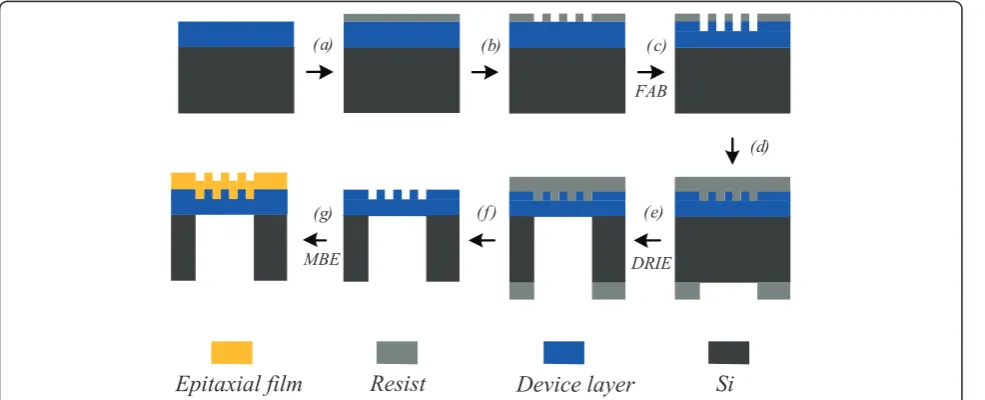
layer (0.70 to approximately 0.20 Al mole fraction), 200-nm AlN buffer layer and 200-μm silicon handle layer. The fabrication process, described in detail else-where [17-19], is schematically illustrated in Figure 1. Nanoscale gratings are patterned in ZEP520A resist using EB lithography, and the resist structures act as a mask for FAB etching of GaN (steps a-b). The Cl2gas is used as the process gas, and the etching depth is about 200 nm (step c). Then the residual EB resist is stripped and the processed device layer is protected by thick photoresist (step d). Silicon substrate beneath the GaN grating region is patterned from backside and etched down to the AlN layer by DRIE, where the AlN layer serves as a definite etch stop (step e). The freestanding GaN gratings are generated by removing the residual photoresist and cleaned for the epitaxial growth (step f). The epitaxial growth is conducted on the processed GaN template by MBE with radio frequency nitrogen plasma as gas source (step g). The epitaxial films with a designed thickness of approximately 420 nm incorporate approximately 140-nm low-temperature buffer layer, approximately 200-nm high-temperature GaN layer, six-pair 3-nm InGaN/9-nm GaN QWs layer and 10-nm GaN top layer. The growth process is described below.
The patterned template is put into a high vacuum cham-ber and cleaned at the temperature of 280°C for 12 h. Then the template is transferred into the growth chamber and cleaned at the temperature of 800°C for 60 min. A 140-nm-thick buffer layer is deposited at the temperature of 700°C, and a 200-nm high-temperature GaN layer is then grown at the temperature of 780°C. The six-pair 3 nm InGaN/9 nm GaN MQWs is subsequently deposited at the temperature of 620 to approximately 640°C.
Finally, a 10-nm GaN layer is grown at the temperature of 620°C.
Experimental results and discussion
Various freestanding GaN gratings are fabricated on a GaN-on-silicon substrate by a combination of EB litho-graphy, FAB etching of GaN and DRIE of silicon [20]. Figure 2 illustrates scanning electron microscope (SEM) images of fabricated freestanding GaN gratings. The grating period and the grating width are expressed by P and W, as shown in Figure 2a, whereP is 500 nm and Wis approximately 300 nm. One period grating consists of the grating ridge and the grating opening. The GaN gratings illustrated in Figure 2b,c,d, have the same grat-ing width of approximately 200 nm and have different grating periods of 500, 450, and 400 nm, respectively. The variation in the grating width Wmeans the differ-ent distributions between the grating ridge and the grat-ing opengrat-ing, which plays an important role in the epitaxial growth.
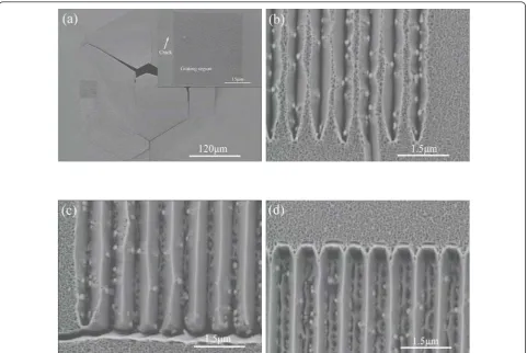
The built-in residual stress in GaN thin film on silicon substrate, which is due to the lattice mismatch and the thermal expansion coefficient mismatch, can result in the deflection problems for freestanding GaN membrane [21]. Although thin GaN membrane can guarantee suffi-cient stiffness for the fabrication of freestanding gratings during DRIE of silicon process, the fracture-related pro-blems are shown in Figure 3a are evident in the free-standing GaN membrane after the epitaxial growth of GaN. These problems might be solved by adjusting the fabrication process. In order to avoid the damage to GaN gratings, the devices are not designed in the centre of the freestanding GaN membrane. The crack networks, which
Si
Device layer
Resist
(a)
(g)
FAB
(f )
(d) (b)
Epitaxial film
MBE
(c)
(e)
[image:2.595.57.550.509.709.2]DRIE
Figure 1Schematical process of patterned growth on freestanding GaN grating by MBE.
Wanget al.Nanoscale Research Letters2011,6:117 http://www.nanoscalereslett.com/content/6/1/117
are caused by the lattice mismatch in the epitaxial layers, are observed on unpatterned GaN substrate, as illustrated in the inset of Figure 3a [22]. The crack does not occur in the GaN grating region, indicating the GaN gratings can compensate the lattice mismatch.
Figure 3b,c,d show the epitaxial structures on the 700-nm-period GaN gratings with the grating widthWof approximately 500, approximately 350, and approxi-mately 250-nm, respectively. Compared with unpatterned GaN substrate, grating structures locally change the dif-fusion conditions of adatoms from neighboring areas. Coherent growth is suppressed, and the selective growth takes place on the grating ridge with a preferential growth process on the low-energy side
{ }
1011 facets. As the grating widthWdecreases, the area of the grating ridge is reduced. Thus, the surface diffusion can be suffi-ciently enhanced, resulting in complete coalescence between two side facets. Epitaxial gratings with smooth facets are observed in Figure 3c,d. Especially, Figure 3d demonstrates that the selective growth can also occur in the grating openings. Compared with Figure 3b, it can be concluded that a critical growth area is needed for theselective growth. When the growth area is too small, the selective growth is suppressed. On the other hand, it’s difficult to complete the selective growth if the growth area is too large. The critical growth area might be dependent on the surface diffusion, which could be improved by adjusting the grating parameters.
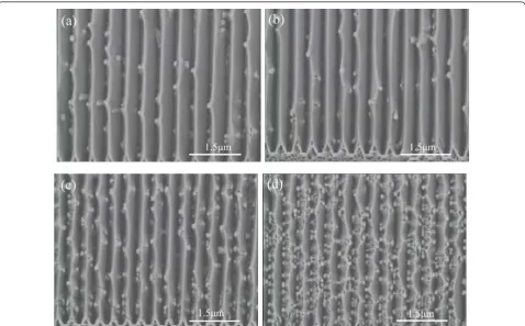
In order to be more specific, we focus our attention on the epitaxial structures grown on the grating ridge. According to the above analysis, small grating period and small grating width are helpful for improving the surface diffusion to realize the selective growth on the grating ridge. On the other hand, nanoscale grating with small grating width is difficult to fabricate. Figure 4a, b shows the epitaxial gratings on the 200-nm-wide GaN grating with the grating periods of 500 and 450 nm, respectively. Coalescences between two side facets are completed for these epitaxial gratings, and side
{ }
1011facets are smooth with random GaN nanocolumns. The epitaxial structures on the 400-nm-period GaN gratings with the grating width Wof approximately 150 nm and approximately 250 nm are illustrated in Figure 4c, d, respectively. The winding of GaN strip is found, which
[image:3.595.57.541.88.410.2]
Figure 2SEMimages of GaN grating templates for the epitaxial growth of GaN.(a)500-nm period, 300-nm-wide grating;(b)500-nm
can be attributed the local fluctuation in the growth process. The number of epitaxial nanocolumns is increased, especially for 250-nm-wide GaN grating.
The shape and the cross section of the epitaxial films are shown in Figure 5. Since the sample is currently used for the development of backside thinning techni-que by wet etching of Al-based compounds, some free-standing epitaxial slabs are damaged in the wet etching process. The measured thickness of epitaxial films is about 510 nm, a little larger than the estimated thick-ness of approximately 420 nm. The freestanding III-nitride slab is deflected due to the residual stress, and the slab is thinner than that on silicon substrate, as shown in Figure 5a. One cross-section image of epitaxial grating is illustrated in Figure 5b. The inset is the zoom-in image of epitaxial grating, and the shape changes are clearly observed on different templates.
The photoluminescence (PL) spectra of the resultant epitaxial gratings are measured at room temperature using a 325-nm He-Cd laser source. The PL of InGaN/GaN QWs deposited on unpatterned area is shown in Figure 6a. Since the silicon substrate is removed and the slab is
thinned by wet etching, the PL intensity is greatly for free-standing InGaN/GaN QWs slab. Figure 6b shows the PL spectra of 700-nm-period epitaxial gratings with various grating widths. The PL peaks at approximately 436.4 nm are associated with the excitation of the InGaN/GaN QWs active layers. With decreasing grating width Wfrom approximately 500 nm to approximately 250 nm, the PL peak and the integrated intensity are significantly increased, corresponding to the improvement in the selec-tive growth. The PL spectra of 500-nm-period epitaxial gratings are shown in Figure 6c and demonstrate the simi-lar optical performances. The PL peaks are about 436.4 nm, and the corresponding PL intensities are improved, indicating that small grating period is helpful for the pat-terned growth. However, the PL spectra illustrated in Fig-ure 6e, f is different as the grating period decreases to 450 and 400 nm, where the number of GaN nanocolumns is gradually increased. Especially for the 400-nm-period epi-taxial gratings, the PL peaks are about 436.4 nm, but the PL intensities are greatly improved with increasing the grating width from approximately 150 nm to approxi-mately 250 nm. However, the PL from 200-nm grating
[image:4.595.58.540.88.410.2]
Figure 3Fracture related problems and epitaxial structures.(a)Epitaxial grating on freestanding GaN membrane, and theinsetis the
zoom-in view of gratzoom-ing region;(b),(c)and(d)the resultant 700-nm period epitaxial gratings:(b)500-nm-wide grating;(c)350-nm-wide grating;(d) 250-nm-wide grating.
Wanget al.Nanoscale Research Letters2011,6:117 http://www.nanoscalereslett.com/content/6/1/117
width sample is stronger than it from 250-nm-grating width sample for the 450-nm-period epitaxial gratings. It might be explained by the formation of epitaxial nanocol-umns. Both epitaxial grating and nanocolumns contribute to the PL excitation. The number of epitaxial nanocol-umns is increased with increasing the grating width, whereas the epitaxial gratings with smooth facets are easily formed with decreasing the grating width. Hence, the
[image:5.595.59.538.88.385.2]epitaxial structures generated in reality determine which one plays the dominant influence on the PL spectra. On the other hand, thin InGaN/GaN QWs layers are incorpo-rated in the upper part of the epitaxial gratings, the film structures beneath smooth side facets are rough, and the scattering losses are thus very large. Consequently, there is no clear signal to reflect the interaction between the excited light and the grating structures.
Figure 4SEM images of the resultant epitaxial gratings.(a)500-nm period, 200-nm-wide grating;(b)450-nm period, 200-nm-wide grating;
(c)400-nm period, 150-nm-wide grating;(d)400-nm period, 250-nm-wide grating.
Figure 5Shape and the cross section of the epitaxial films.(a)The cross section of the epitaxial films;(b)freestanding epitaxial grating
[image:5.595.59.541.555.702.2]Conclusions
In summary, various freestanding GaN gratings are fab-ricated on a GaN-on-silicon substrate by a combination of EB lithography, FAB etching of GaN and DRIE of sili-con. The patterned growth of InGaN/GaN QWs is per-formed on the processed GaN template by MBE. Nanoscale grating structures locally change the diffusion conditions of adatoms from neighboring areas, and the selective growth takes place with a preferential growth process on the low-energy side facets. Coalescences between two side facets are achieved to generate epitax-ial gratings with triangular section, and the patterned growth depends on the grating periodP and the grating widthW. Thin epitaxial gratings produce the promising photoluminescence performance. This work provides a feasible way for further GaN-based integrated optics
devices by a combination of GaN micromachining and MBE growth on a GaN-on-silicon substrate.
Acknowledgements
This work was supported by the Research Project, Grant-In-Aid for Scientific Research (19106007). Yongjin Wang gratefully acknowledges the Japan Society for the Promotion of Science (JSPS) for financial support.
Authors’contributions
YW carried out the device design and fabrication, performed the optical measurements, and drafted the manuscript. FH carried out the MBE growth. KH conceived of the study, and participated in its design and coordination. All authors read and approved the final manuscript.
Competing interests
The authors declare that they have no competing interests.
Received: 7 September 2010 Accepted: 4 February 2011 Published: 4 February 2011
300 400 500 600 700 0 1000 2000 3000 4000 5000 PL Int en si ty (a.u.) Wavelength (nm)
Period P-Width W
700nm-500nm 700nm-350nm 700nm-250nm
(b) 436.4nm
300 400 500 600 700 0 2000 4000 6000 8000 PL I nt ens ity ( a.u.) Wavelength (nm)
Period P-WidthW
500nm-300nm 500nm-250nm 500nm-200nm
(c)
300 400 500 600 700 0 2000 4000 6000 8000 10000 12000 14000 (d) PL I nt en sit y ( a.u.) Wavelength (nm)
Period P-Width W
450nm-300nm 450nm-250nm 450nm-200nm
300 400 500 600 700 0 2000 4000 6000 8000 10000 (e) PL I nt ens ity (a.u.) Wavelength (nm)
Period P-Width W
400nm-250nm 400nm-200nm 400nm-150nm
300 400 500 600 700 0
2000 4000 6000
PL Intensity (a.u.)
Wavelength (nm)
InGaN/GaN QWs slab InGaN/GaN QWs on Si
[image:6.595.60.538.89.490.2](a)
Figure 6Photoluminescence (PL) spectra of the resultant epitaxial gratings.(a)PL spectra of epitaxial films on unpatterned template;
(b)-(e)PL spectra of the resultant epitaxial gratings:(b)700-nm-period gratings;(c)500-nm-period gratings;(d)450-nm-period gratings; (e)400-nm-period gratings.
Wanget al.Nanoscale Research Letters2011,6:117 http://www.nanoscalereslett.com/content/6/1/117
References
1. Kato Y, Kitamura S, Hiramatsu K, Sawaki N:Selective growth of wurtzite GaN and AlxGa1--xN on GaN/sapphire substrates by metalorganic vapor
phase epitaxy.J Cryst Growth1994,144:133-140.
2. Akasaka T, Kobayashi Y, Ando S, Kobayashi N:GaN hexagonal microprisms with smooth vertical facets fabricated by selective metalorganic vapor phase epitaxy.Appl Phys Lett1997,71:2196-2198.
3. Beaumont B, Gibart P, Vaille M, Haffouz S, Nataf G, Bouillé A:Lateral overgrowth of GaN on patterned GaN/sapphire substrate via selective metal organic vapour phase epitaxy: a route to produce self supported GaN substrates.J Cryst Growth1998,189/190:97-102.
4. Matsubara H, Yoshimoto S, Saito H, Yue JL, Tanaka Y, Noda S:GaN Photonic-Crystal Surface-Emitting Laser at Blue-Violet Wavelengths.
Science2008,319:445-447.
5. Nataf G, Beaumont B, Bouillé A, Haffouz S, Vaille M, Gibart P:Lateral overgrowth of high quality GaN layers on GaN/Al2O3patterned
substrates by halide vapour-phase epitaxy.J Cryst Growth1998,
192:73-78.
6. Wagner V, Parillaud O, Bühlmann HJ, Ilegems M, Gradecak S, Stadelmann P, Riemann T, Christen J:Influence of the carrier gas composition on morphology, dislocations, and microscopic luminescence properties of selectively grown GaN by hydride vapor phase epitaxy.J Appl Phys2002,
92:1307-1316.
7. Zeng KC, Lin JY, Jiang HX, Yang W:Optical properties of GaN pyramids.
Appl Phys Lett1999,74:1227-1229.
8. Ren DW, Zhou W, Dapkus PD:Low-dislocation-density, nonplanar GaN templates for buried heterostructure lasers grown by lateral epitaxial overgrowth.Appl Phys Lett2005,86:111901.
9. Zang KY, Wang YD, Chua SJ, Wang LS:Nanoscale lateral epitaxial overgrowth of GaN on Si (111).Appl Phys Lett2005,87:193106. 10. Application Note 11: Substrates for GaN RF devices.[http://www.nitronex.
com/].
11. Tang H, Bardwell JA, Webb JB, Moisa S, Fraser J, Rolfe S:Selective growth of GaN on a SiC substrate patterned with an AlN seed layer by ammonia molecular-beam epitaxy.Appl Phys Lett2001,79:2764-2766. 12. Ruterana P, Albrecht M, Neugebauer J:Nitride Semiconductors: Handbook on
Materials and DevicesWeinheim: Wiley; 2003.
13. Stoica T, Sutter E, Meijers RJ, Debnath RK, Calarco R, Lüth L, Grützmacher D:
Interface and wetting layer effect on the catalyst-free nucleation and growth of GaN nanowires.Small2008,4:751.
14. Wang YJ, Hu FR, Hane K:Freestanding GaN slab fabricated on patterned silicon on an insulator substrate.J Micromech Microeng2010,20:027001. 15. Kikuchi A, Kawai M, Tada M, Kishino K:InGaN/GaN Multiple Quantum Disk
Nanocolumn Light-Emitting Diodes Grown on (111) Si Substrate.Jpn J Appl Phys2004,43:L1524.
16. Kishino K, Sekiguchi H, Kikuchi A:Improved Ti-mask selective-area growth (SAG) by rf-plasma-assisted molecular beam epitaxy demonstrating extremely uniform GaN nanocolumn arrays.J Cryst Growth2009,
311:2063-2068.
17. Wang YJ, Hu FR, Hane K:Nanoscale epitaxial growth of GaN on freestanding circular GaN grating.IEEE Optical MEMS & Nanophotonics 2010.
18. Wang YJ, Hu FR, Sameshima H, Hane K:Fabrication and characterization of freestanding circular GaN gratings.Opt Express2010,18:773-779. 19. Wang YJ, Hu FR, Kanamori Y, Sameshima H, Hane K:Fabrication and
characterization of subwavelength nanostructures on freestanding GaN slab.Opt Express2010,18:2940-2945.
20. Wang YJ, Hu FR, Wakui M, Hane K:Freestanding GaN resonant gratings at telecommunication range.IEEE Photon Technol Lett2009,21:1184-1186. 21. Lv J, Yang ZC, Yan GZ, Lin WK, Cai Y, Zhang BS, Chen KJ:Fabrication of Large-Area Suspended MEMS Structures Using GaN-on-Si Platform.IEEE Electron Device Lett2009,30:1045-1047.
22. Bethoux JM, Vennéguès P, Natali F, Feltin E, Tottereau O, Nataf G, De Mierry P, Semond F:Growth of high quality crack-free AlGaN films on GaN templates using plastic relaxation through buried cracks.J Appl Phys2003,94:6499-6507.
doi:10.1186/1556-276X-6-117
Cite this article as:Wanget al.:Patterned growth of InGaN/GaN quantum wells on freestanding GaN grating by molecular beam epitaxy.Nanoscale Research Letters20116:117.
Submit your manuscript to a
journal and benefi t from:
7Convenient online submission
7Rigorous peer review
7Immediate publication on acceptance
7Open access: articles freely available online
7High visibility within the fi eld
7Retaining the copyright to your article