Technology (IJRASET)
Analysis of Single-Input Multiple-Output DC–DC
Converter
B. Uma Maheswara Rao1, K. Nagalingachari 2
1
M. Tech scholar, 2Assistant professor Department of EEE
LakkiReddy BaliReddy College of Eengineering, Vijayawada, India
Abstract: - The aim of this study is to develop a closed loop single-input multiple-output (SIMO) dc–dc converter. The proposed converter can increase the voltage of a low level voltage input power source to a controllable high level voltage dc bus and mid-level voltage output terminals. The high mid-level voltage dc bus can take as the main power for a high mid-level voltage dc load or for a dc–ac inverter. Moreover, mid-level voltage output terminals can supply powers for individual mid-level voltage dc loads or for charging auxiliary power sources (e.g., battery modules). In this study, a coupled-inductor based dc–dc converter utilizes only one power switch with the corresponding device specifications are adequately designed. As a result, the objectives of high-efficiency power conversion, high step up ratio, and various output voltages with different levels can be achieved.
Index Terms:- Coupled inductor, power conversion, single-input multiple-output (SIMO) converter voltage clamping.
I. INTRODUCTION
Technology (IJRASET)
and analyses are given in Section II. In Section III, the design considerations of the proposed SIMO converter are discussed in detail. Section IV provides simulation results of proposed converter.
II. CONVERTER DESIGN AND ANALYSES
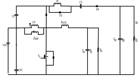
The system configuration of the proposed high-efficiency SIMO converter topology to generate two different voltage levels from a single-input power source is depicted in Fig. 1. This SIMO converter contains five parts including a low-voltage-side circuit (LVSC), a clamped circuit, a middle-voltage circuit, an auxiliary circuit, and a high-voltage-side circuit (HVSC). The major symbol representations are summarized as follows. VFC (iFC ) and VO1 (iO1) denote the voltages (currents) of the input power source and the output load at the LVSC and the auxiliary circuit, respectively; VO2 and iO2 are the output voltage and cur-rent in the HVSC. CFC , CO1 , and CO2 are the filter capacitors at the LVSC, the auxiliary circuit, and the HVSC, respectively; C1and C2are the clamped and middle-voltage capacitors inthe clamped and middle-voltage circuits, respectively. LP and LSrepresent individual inductors in
the primary and secondarysides of the coupled inductor Tr , respectively, where the primary side is connected to the input power
source; Laux is the auxiliary circuit inductor. The main switch is expressed as S1 in the LVSC; the equivalent load in the auxiliary circuit is represented as RO1 and the output load is represented as RO2 in the HVSC. The corresponding equivalent circuit given in Fig. 2 is used to define the voltage polarities and current directions. The coupled inductor in Fig. 1 can be modelled as an ideal transformer including the magnetizing inductor Lm p and the leakage inductor Lk p in Fig. 2. The turn’s ratio N and coupling coefficient k of this ideal transformer are defined as
N = N2/N1 (1)
k = Lmp/(Lkp + Lmp) = Lmp/LP (2)
Where N1 and N2 are the winding turns in the primary and secondary sides of the coupled inductor Tr .
Fig. 1.System configuration of input multiple-output (SIMO) converter.
Because the voltage gain is less sensitive to the coupling coefficient and the clamped capacitor C1 is appropriately selected to completely absorb the leakage inductor energy [13], the coupling coefficient could be simply set at one (k = 1) to obtain Lm p = LP
via (2). In this study, the following assumptions are made to simplify the converter analyses: 1) The main switch including its body diode is assumed to be an ideal switching element; and 2) The conduction voltage drops of the switch and diodes are neglected.
R D2 C2 D4 LP CFC VFC C1 AUX L C 01 01 V 01 C
02 R02 V
[image:3.612.188.426.363.490.2] [image:3.612.186.422.577.706.2]Technology (IJRASET)
A. Operation Modes
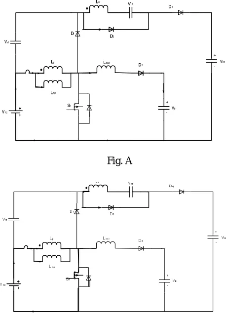
The characteristic waveforms are depicted in Fig. 3, and the topological modes in one switching cycle are illustrated in Fig. 4.
1) Mode 1 (t0 –t1 ) [Fig. 4(a)]: In this mode, the main switch S1 was turned ON for a span, and the diode D4 turned OFF. Because
the polarity of the windings of the coupled inductor Tr is positive, the diode D3 turns ON. The secondary current iL s reverses and charges to the middle-voltage capacitor C2 . When the auxiliary inductor Laux releases its stored energy completely, and the diode D2 turns OFF, this mode ends.
2) Mode 2 (t1 –t2 ) [Fig. 4(b)]: At time t = t1 , the main switch S1 is persistently turned ON. Because the primary inductor LP is
charged by the input power source, the magnetizing current iLmp increases gradually in an approximately linear way. At the same time, the secondary voltage vL s charges the middle-voltage capacitor C2 through the diode D3 . Although the voltage vL m p is equal to the input volt-age VFC both at modes 1 and 2, the ascendant slope of the leakage current of the coupled inductor (diL k p /dt) at modes 1 and 2 is different due to the path of the auxiliary circuit. Because the auxiliary inductor Laux releases its stored energy completely, and the diode D2 turns OFF at the end of mode 1, it results in the reduction of diL k p /dt at mode 2.
3) Mode 3 (t2 –t3 ) [Fig. 4(c)]: At time t = t2 , the main switch
S1 is turned OFF. When the leakage energy still released from the secondary side of the coupled inductor, the diode D3 persistently conducts and releases the leakage energy to the middle-voltage capacitor C2 . When the voltage across the main switch vS 1 is higher than the voltage across the clamped capacitor VC 1 , the diode D1 conducts to transmit the energy of the primary-side leakage inductor Lk p into the clamped capacitor C1 . At the same time, partial energy of the primary-side leakage inductor Lk p is transmitted to the auxiliary inductor Laux , and the diode D2 conducts. Thus, the current iL aux passes through the diode D2 to supply the power for the output load in the auxiliary circuit. When the secondary side of the coupled inductor releases its leakage energy completely, and the diode D3 turns OFF, this mode ends.
4)Mode 4 (t3 –t4 ) [Fig. 4(d)]: At time t = t3 , the main switch S1 is persistently turned OFF. When the leakage energy has released
from the primary side of the coupled inductor, the secondary current iL S is induced in reverse from the energy of the magnetizing inductor Lm p through the ideal transformer, and flows through the diode D4 to the HVSC. At the same time, partial energy of the primary-side leakage inductor Lk p is still persistently transmitted to the auxiliary inductor Laux , and the diode D2 keeps to conduct. Moreover, the current iL aux passes through the diode D2 to supply the power for the output load in the auxiliary circuit.
Technology (IJRASET)
5) Mode 5 (t4 –t5 ) [Fig. 4(e)]: At time t = t4 , the main switch S1 is persistently turned OFF, and the clamped diode D1 turns OFF
because the primary leakage current iL k p equals to the auxiliary inductor current iL aux . In this mode, the input power source, the primary winding of the coupled inductor Tr , and the auxiliary inductor Laux connect in series to supply the power for the output load in the auxiliary circuit through the diode D2 . At the same time, the input power source, the secondary winding of the coupled inductor Tr , the clamped capacitor C1 , and the middle-voltage capacitor (C2 ) connect in series to release the energy into the HVSC through the diode D4 .
6) Mode 6 (t5 –t6 ) [Fig. 4(f)]: At time t = t5 , this mode begins when the main switch S1 is triggered. The auxiliary inductor current
iL aux needs time to decay to zero, the diode D2 persistently conducts. In this mode, the input power source, the clamped capacitor C1, the secondary winding of the coupled inductor Tr , and the middle-voltage capacitor C2 still connect in series to release the energy into the HVSC through the diode D4 . Since the clamped diode D1 can be selected as a low-voltage Schottky diode, it will be cut off promptly without a reverse-recovery current. Moreover, the rising rate of the primary current iLkp is limited by the primary-side leakage inductor Lkp . Thus, one cannot derive any currents from the paths of the HVSC, the middle-voltage circuit, the auxiliary circuit, and the clamped circuit. As a result, the main switch S1 is turned ON under the condition of ZCS and this soft-switching property is helpful for alleviating the soft-switching loss. When the secondary current iL S decays to zero, this mode ends. After that, it begins the next switching cycle and repeats the operation in mode 1.
Remark 1: In general, a dc–dc converter operated at the continuous conduction mode (CCM) can provide a low ripple cur-rent for
[image:5.612.185.414.376.697.2]protecting the energy source. In the proposed SIMO converter, it is operated at the CCM due to the design of the auxiliary inductor. The coupled inductor is charged by the in-put power source when the main switch is turned ON, and the coupled inductor releases its energy to the auxiliary inductor when the main switch is turned OFF until the energy balance of the coupled inductor and the auxiliary inductor is established. As can be seen from Fig. 3, the primary current of the coupled inductor is positive during one switching cycle. This CCM operation is helpful to extend the lifetime of the input energy source.
Fig. A
Technology (IJRASET)
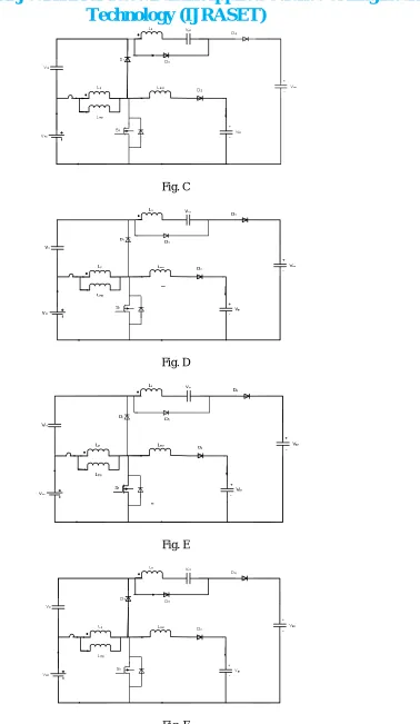
Fig. C
Fig. D
Fig. E
Technology (IJRASET)
Fig.4. Topological modes: (a) Mode 1 [t0−t1 ]; (b) Mode 2 [t1−t2 ]; (c) Mode 3 [t2−t3 ]; (d) Mode 4 [t3−t4 ]; (e) Mode 5 [t4−t5 ];
(f) Mode 6 [t5−t6 ].
B. Control Method
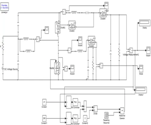
Fig 5 shows the closed loop control of SIMO DC-DC Converter in which both the output voltages are compared with reference values. After comparing, produced error is processed through two PI controllers then two processed signals are averaged and fed to PWM generator. By connecting PWM pulses to the switch of the converter we can get controllable output voltages at output stages. This technique can be used for multiple outputs DC-DC Converter.
SIMO DC-DC Converter
compare
compare
PI1
PI2
Average V01
V02
PWM
PWM V01
V01 ref
V02
V02 ref
Fig 5 closed loop control
III. SIMULATION RESULTS
[image:7.612.178.428.412.620.2]In this section the simulation results are presented.
Fig 6 Simulink Model of Proposed SIMO DC-DC Converter
Technology (IJRASET)
Fig 7A
Fig 7B
Kp Ki
PI1 5e-4 5e-4
PI2 5e-5 5e-5
Table 1 shows PI controller gains for closed loop SIMO Converter
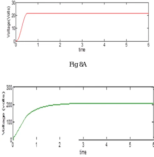
[image:8.612.181.428.448.699.2]Fig 8 (a)&(b) shows controlled output voltages at auxiliary circuit and high voltage circuit respectively.
Technology (IJRASET)
12 V I/P Reference Achieved
V01 21 21.02
[image:9.612.179.433.176.378.2]V02 205 205.2
Table 2 presents the accuracy of closed loop control of Proposed converter.
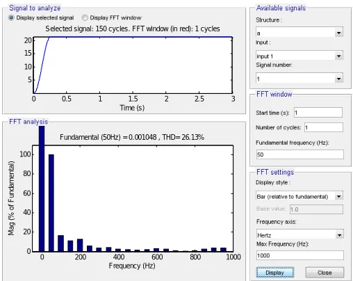
Fig 9 FFT analysis of the SIMO converter
IV. CONCLUSION
Proposed converter configuration provides controllable voltage levels at different output terminals. This converter can be used in renewable energy sources like Fuel Cell, Solar, wind e t c,. This converter can be connected to any kind of loads and/or inverters are an added advantage.
REFERENCES
[1] A. Kirubakaran, S. Jain, and R. K. Nema, “DSP-controlled power electronic interface for fuel-cell-based distributed generation,” IEEE Trans.Power Electron., vol. 26, no. 12, pp. 3853–3864, Dec. 2011.
[2] B. Liu, S. Duan, and T. Cai, “Photovoltaic dc-building-module-based BIPV system-concept and design considerations,” IEEE Trans. Power Electron., vol. 26, no. 5, pp. 1418–1429, May 2011.
[3] M. Singh and A. Chandra, “Application of adaptive network-based fuzzy interference system for sensor less control of PMSG-based wind turbine with nonlinear-load-compensation capabilities,” IEEE Trans. Power Electron., vol. 26, no. 1, pp. 165–175, Jan. 2011.
[4] C. T. Pan,M. C. Cheng, and C.M. Lai, “A novel integrated dc/ac converter with high voltage gain capability for distributed energy resource systems,” IEEE Trans. Power Electron., vol. 27, no. 5, pp. 2385–2395, May 2012.
[5] S. D. Gamini Jayasinghe, D. Mahinda Vilathgamuwa, and U. K. Madawala, “Diode-clamped three-level inverter-based battery/ supercapacitor direct integration scheme for renewable energy systems,” IEEE Trans. Power Electron., vol. 26, no. 6, pp. 3720–3729, Dec. 2011.
[6] H.Wu, R. Chen, J. Zhang, Y. Xing, H. Hu, and H. Ge, “A family of three port half-bridge converters for a stand-alone renewable power system,” IEEE Trans. Power Electron., vol. 26, no. 9, pp. 2697–2706, Sep. 2012.
[7] M. W. Ellis, M. R. Von Spakovsky, and D. J. Nelson, “Fuel cell systems: Efficient, flexible energy conversion for the 21 st century,” Proc. IEEE, vol. 89, no. 12, pp. 1808–1818, Dec. 2001.
[8] T. Kim, O. Vodyakho, and J. Yang, “Fuel cell hybrid electronic scooter,” IEEE Ind. Appl. Mag., vol. 17, no. 2, pp. 25–31, Mar./Apr. 2011.
[9] F. Gao, B. Blunier, M. G. Sim˜oes, and A. Miraoui, “PEM fuel cell stack modeling for real-time emulation in hardware-in-the-loop application,” IEEE Trans. Energy Convers., vol. 26, no. 1, pp. 184–194, Mar. 2011.
[10] P. Patra, A. Patra, and N. Misra, “A single-inductor multiple-output switcher with simultaneous buck, boost and inverted outputs,” IEEE Trans. Power Electron., vol. 27, no. 4, pp. 1936–1951, Apr. 2012.
[11] A. Nami, F. Zare, A. Ghosh, and F. Blaabjerg, “Multiple-output DC–DC converters based on diode-clamped converters configuration: Topology and control
0 0.5 1 1.5 2 2.5 3
5 10 15 20
Selected signal: 150 cycles. FFT window (in red): 1 cycles
Time (s)
0 200 400 600 800 1000
0 20 40 60 80 100 Frequency (Hz)
Fundamental (50Hz) = 0.001048 , THD= 26.13%
Technology (IJRASET)
strategy,” IET Power Electron., vol. 3, no. 2, pp. 197–208, 2010.[12] Y. Chen, Y. Kang, S. Nie, and X. Pei, “The multiple-output DC–DC converter with shared ZCS lagging leg,” IEEE Trans. Power Electron., vol. 26, no. 8, pp. 2278–2294, Aug. 2011.
[13] R. J.Wai and R. Y. Duan, “High step-up converter with coupled inductor,” IEEE Trans. Power Electron., vol. 20, no. 5, pp. 1025–1035, Sep. 2005. [14] N. Mohan, T. M. Undeland, and W. P. Robbins, Power Electronics: Converters, Applications, and Design. New York: Wiley, 1995.
[15] L. Schuch, C. Rech, H. L. Hey, H. A. Gr¨undling, H. Pinheiro, and J. R. Pinheiro, “Analysis and design of a new high-efficiency bidirectional integrated ZVT PWM converter for DC-bus and battery-bank interface,” IEEE Trans. Ind. Appl., vol. 42, no. 5, pp. 1321–1332, Sep./Oct. 2006.
[16] Y. Chen and Y. Kang, “A full regulated dual-output dc-dc converter with special-connected two transformers (SCTTs) cell and complementary pulsewidth modulation-PFM(CPWM-PFM),” IEEE Trans. Power Electron., vol. 25, no. 5, pp. 1296–1309, May 2010.
[17] J. K. Kim, S.W. Choi, and G.W. Moon, “Zero-voltage switching postregulation scheme for multioutput forward converter with synchronous switches,” IEEE Trans. Ind. Electron., vol. 58, no. 6, pp. 2378–2386, Jun. 2011.
[18] L. Hang, S. Wang, Y. Gu, W. Yao, and Z. Lu, “High cross-regulation multi output LLC series resonant converter with Magamp postregulator,” IEEE Trans. Ind. Electron., vol. 58, no. 9, pp. 3905–3913, Sep. 2011.
[19] S. H. Cho, C. S. Kim, and S. K. Han, “High-efficiency and low-cost tightly regulated dual-output LLC resonant converter,” IEEE Trans. Ind. Electron., vol. 59, no. 7, pp. 2982–2991, Jul. 2012
B.UMA MAHESWARA RAO is currently pursuing M.Tech in Power Electronics and Drives in Lakireddy Balireddy College of Engineering, Mylavaram. He received B.Tech degree in Electrical and Electronics Engineering from SRIST, Khammam in the year 2013. His areas of interest are Renewable Energy Resources and DC-DC converters.
K.NAGALINGACHARI received M.Tech.degree in Newtons Instistute of Engineering,Guntur in the year 2013. He obtained B.Tech degree in Electrical and Electronics Engineering from Newtons Instistute of Engineering,Guntur in the year 2008. His is presently working as Assistant professor in Lakireddy Balireddy college of engineering, Mylavaram. His areas of interest are power electronic