Designing a Sustaining Amplifier for a 17.22 MHz
Electrostatic Resonator based Reference Oscillator
Sukanta Roy, Dr. Harikrishnan Ramiah and Dr. Ahmed Wasif Reza
Department of Electrical Engineering, Faculty of Engineering, University of Malaya, Kuala Lumpur, Malaysia
Abstract: MEMS resonator based oscillators, however, are now a
technical reality which are extremely cost-effective, very small in size in comparison with quartz crystal based oscillators and can be fabricated in the conventional CMOS process, monolithically. In this work a new sustaining amplifier is designed for a 17.22 MHz MEMS resonator which has an unloaded quality factor of 1000. A total transimpedance open loop gain of 122 dB-Ω has been achieved over the bandwidth of interest to drive this resonator for a sustained oscillation. Total DC power consumption of this sustaining amplifier is 6.3mW from a 1.8v DC source in 0.18μm CMOS process.
Keywords: Electrostatic resonator, MEMS, TIA, 0.18μm CMOS,
Sustaining amplifier.
1.
Introduction
Most electronic systems, such as frequency synthesizers, filters, noise suppressor, harmonic filter, etc. need some type of reference clocking signal generators. These are known as reference oscillators. In recent years of compact IC fabrication and hardware revolution, to support for a high level of integration is so limited toconventional circuits. Because, conventional high quality frequency reference circuitry usually employs quartz crystal and crystal cannot be manufactured in chip fabrication processes and also, it consumes a considerable space in the circuit board. To find the solution, extensive research has been led to the technologies of bulk acoustic wave (BAW) resonators [1], micro-electromechanical systems (MEMS) resonators[3-4] and surface acoustic wave (SAW) resonators[2], as the alternate of quartz crystal.
In preference, there are MEMS resonators which exhibit Q-factors as high as 4,400 which are close to those of crystals Q factor [4].In a penalty paid in temperature stability and aging, MEMS based resonators are generating interest in monolithic system-on-chip (SOC) fabrication CMOS processes which will decrease the form factors, substantially [4].In this work, a fixed frequency reference oscillator is assigned and implemented using a clamped-clamped (CC) beam MEMS resonators. Generally, MEMS resonator inherits losses in energy, grouped from a number of sources such as anchor loss, air damping, vibrational etc. As illustrated in Fig. 1, after being fabricated on silicon (Si) substrate a ‘clamped-clamped beam’ resonator is actually a vibrating beam. The transducer gap between the beam and electrodes are used to drive this vibration into resonance which alsocreates a very high motional resistance (in approximate to about mega-ohm or even greater, depending
upon the physical structures). Now, to sustain this resonance this resistance would be replenishedby a sufficient gain in feedback configuration.
In this work, a sustaining amplifier is designed which will satisfy the gain and bandwidth requirements, complementing to Barkhausen criterion to replenish this motional losses highlighted above. The resonator’s functionalityis demonstrated by implementing a CMOS single endedreference oscillator where the resonator should define a 17.22 MHz operating frequency.In the following parts, Section 2presents the characteristics and the equivalent model of the MEMS resonator. Section 3describes the designed sustaining amplifier circuit block-by-block and Section 4 dictates resonator model parameters, required amplification specifications and the open-loop responses collectedfrom AC analysis of the sustaining amplifier.
2.
MEMS resonator and electrical modelling
[image:1.595.314.549.534.697.2]The type of the resonator utilized here, is an electrostatic clamp-clamp (CC) beam type and it is fabricated on Si substrate by Silterra Malaysia Sdn. Bhd. Physically, it has two electrodes; one for excitation and the other for read-out where an external 5V DC is fed to it for activation. In Fig. 1, a CC beam resonator schematic is illustrated with its flexural mode of beam movement as shown explicitly.
Figure 1.(a) A Clamp-clamp beam resonator (b) its motional direction (c) electrical model of it [3]
electrical model with a lower motional resistance and lower resonance frequency.
Now, resonators have distributed mass and spring. So, for a system analysis, lumped mass spring model is preferred. In describing the resonator electrical characteristics and motional behavior, a two electrode configuration is often derived which is developed from Euler-Bernoulli (E-B) equation of movement for this mass-spring model of vibrating beam.
For a single electrode CC resonator, the E-B equation is given as in Eqn. (1),which is derived in time domain from the flexural shape of beam vibration seen in Fig. 1(b).
t i tot
eff kU x F
t x U t x U
m
) ( . ) ( ) ( 2 2 (1)
x tot x x AC
eff V dt I k I t I m
(2)where g C V t x U I DC x 0 ) (
, is “electromechanical coupling
factor” which is needed to be introduced as to convert the excitation voltage, VAC into force, F and convert the
mechanical displacement, Ux into signal current, Ix. For these
conversions, there are basically two types of transduction methods available,namely, capacitive and piezoelectric transduction. In this work, the signal current is produced by capacitive transduction.Now, the following terms are defined to draw an analogy in between mechanical resonator and its electrical model.
‘meff’ is the effective mass which is the apparent mass,
which depends on the position and velocity throughout the vibrating length, L. It is generating inertiawhich is like an inductor in electrical analogy,to produce capacitive currentIx.
The expression of effective is as follows:
U dV A U xdx A L
m
L
eff ( ) 0.40 * *
0 1 2 2
tot Damping coefficient (spring mass system) equivalent to the resistance and losses in electrical analogy,k= Stiffness of the mechanical beam,U(x) = Mode shape for the mechanical displacement,x,I(x)=Time derivative of U(x)for using in electrical analogy of a capacitive transduction,F= Amplitude of the exerted force which is likewise VAC, in
electrical excitation case.From Eqn.(2), we get:
AC x x tot x eff V dt I k I t I m
2 2 2 (3)The RLC series circuit as described in Fig.1(c) has the response of: AC x x x x x
x I dt V
C I R t I
L
1
(4)
So, it can be seen Eqn. (3) is comparable with a series RLC characteristic of Eqn. (4) based on which, an electrical model representation of the resonator is drawn in Fig. 1(c). In Section 4 this series RLC electrical model along with lumped parameters is presented. The values are extracted through curve fitting technique fromans-parameter analysis and measurement data froma spectrum analyser (VNA).
3.
Sustaining amplifier
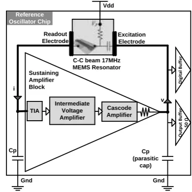
Sustaining amplifier has an adequate gain-bandwidth product tocompensate the losses of damped oscillation originating from a resonator and hence, make it sustaining in time domain. Precisely, the sustaining amplifier will provide the exact amount of negative resistance to compensate the loss in resonator and grow the oscillation and subsequently sustain it in time with a fixed amplitude and frequency. Figure 2 demonstrates the basic blocks of such a ‘MEMS based reference oscillator’ system.
[image:2.595.331.526.208.402.2]TIA Intermediate Voltage Amplifier Cascode Amplifier C-C beam 17MHz MEMS Resonator O u tp u t B u ff e r 5 0 Ω D ig it al B u ff e r Cp Cp (parasitic cap) Excitation Electrode Readout Electrode Reference Oscillator Chip Sustaining Amplifier Block i v Vdd Gnd Gnd
Figure 2.Sustaining amplifier block in close loop in an oscillator chip
An external Vp is needed for one of the MEMS electrodes
and a read-out signal VACis fed back through the feedback
path to the other electrode of it, for initiating a resultant force between them. This creates a displacement which will initiate a capacitive transduction and will produce a capacitive current. As shown in Fig. 2, a transimpedance amplifier (TIA) will convert this tiny displacement current into a voltage signal and in consecutive voltage amplifier blocks (intermediate VA and cascode amplifier) a net high gain would make this signal sustain at the excitation electrode of the MEMS. In this way, in the feedback loop, the sustaining amplifier would ensure the necessary loss compensation by a tuned Gain-BW product. Additionally, AGC (automatic gain control) block can beintegratedin improving the oscillation properties such as phase noise, tuning ability, variable gain, etc. For measuring purposes, there are output buffer amplifiers to drive at least 50Ω impedances such that, it could not load the original alternating voltage signal. The sustaining block designed in this work contains three stages: transimpedance amplifier (TIA), intermediate voltage amplifier and a high gain cascode amplifier. The oscillation output (voltage signal) is extracted out through the 50Ωoutput buffer (unity gain) amplifier. In this regard, a detailed demonstration of each of the blocks is given.
3.1 TransimpedanceAmplifier (TIA):
The designed TIA, with a high transimpedance gain is the first stage in this MEMS resonator based oscillator circuit (Fig. 3).
R1
R2 R3
R4
M1 M2
M4 M3
TIA_out, mV Vdd
[image:3.595.376.500.65.220.2]Current from resonator, nA
Figure 3.Designed Transimpedance Amplifier
In the operation of a resonator, an interaction between the DC and AC component of the signal, which are the inputs of the resonator will initiate some mechanical force and the capacitive reaction from this vibrational displacement will be read-out as a capacitive current in the resonators electrode [6-7]. The sensed currentis much lower in amplitude and there is a need of high gain amplifier compensation. Also, the input and output impedance need to be as low as possible to avoid the loading at the resonator I/O by the amplifier. Hence, an amplifying circuit which will convert the resonator current into voltage is designed (Fig. 3),which can give us certain features asgiven below:
Low input and output impedance.
High gain in converting input current to a voltage signal.
Outlays room to addvoltage amplifiers as the subsequent stages for additional gain and control.
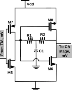
3.2 Intermediate Voltage Amplifier:
The intermediate voltage amplifier designed here is intended to add more voltage gain with minimal phase shift (Fig. 4).
There are some inherent losses in a resonator based oscillator design where the prime sources can be named down to:
‘Output buffer circuit’ which is mandatory in the characterization of the oscillator with the minimum signal reflection.
‘On-Chip connectors’which are used in between different blocks for interconnection.
So, the intermediate voltage amplifier as the second stage will compensate these losses by exact voltage gain with sufficient bandwidth. The design in Fig. 4 has been emphasized in obtaining a zero or 360o total phase shift at the output while complimenting the Barkhausen criterion round the entire loop of sustaining amplifier. Barkhausen criterion is a necessary condition to meet for oscillator theory, though it may not be all adequate in some cases too.
M5
M6
M7 M8
Vdd
R1 R2
C1
To CA stage, mV
F
ro
m
T
IA
,
m
V
Figure4.Designed intermediate voltage amplifier (a modified Cherry-Hooper amplifier)
In alliance to the above mentioned criterion, a modified Cherry-Hooper amplifier is chosen its enhancing ability to gain and bandwidth separately. Also, push-pull inverter topology is chosen among various topologies to make it simpler to give more output with less distortion per active device. In between two stages, the second stage is the gain tuning stage by designing R2-C1 ‘T’ network. This ‘T’ network in this shunt-shunt feedback will introduce an extra zero, which will be used in for pole cancellation and will offer less input and output impedance of the next stage. Also, as this R2-C1 will try to shift the poles to higher frequency, so bandwidth will also be increased.Also, linearity will also be increased for preceding TIA stage.
3.3 Cascode Amplifier:
The final stage designed and integrated in the sustaining amplifier topology is a high gain cascode amplifier which will further boost the voltage with a necessary phase shift in order to drive the resonator in a close loop configuration (Fig. 5).
Decoupling capacitor, C2 R5 R6
R7
M9
M10 M11 M12 M14 M13
F
ro
m
p
re
v
io
u
s
v
o
lt
a
g
e
a
m
p
p
li
fi
e
r
s
ta
g
e
,
m
V
Vdd
O
u
tp
u
t
v
o
lt
a
g
e
,
m
V
(a
c
ts
a
s
V
a
c
f
o
r
th
e
re
s
o
n
a
to
r
in
c
lo
s
e
l
o
o
p
[image:3.595.125.234.65.250.2])
Figure 5. Designed high gain Cascode voltage amplifier with biasing
Cascode (common source with common gate) structure is chosen here among other topology as to have a high gain, high input impedance and a reduced Miller effect (by CS), which can also ensure an enhanced bandwidth.
characteristics for producing an acceptable reference signal [3]. It should have a high gain to replenish the resonator loss (more than 1.5 times of resonator’s motional resistance) [3] and a bandwidth which is larger than the resonator frequency by a certain magnitude that actually ensures a small phase shift around the feedback loop. Also, a low input and output impedance should be ensured to avoid loading the resonator and it will ensure lower phase noises too. The automatic gain control mechanism is also frequently adapted to prevent uncontrolled growing oscillation, but, this can be avoided by employing a feedback control.
In the present design, TIA module produces an amplified voltage output signal from the resonator’s output current signal while the combination of M3, M4, R2 and R4. Here, M1, M2, R1 are producing the bias current throughout the rest of the functional circuit. The modified Cherry-Hooper amplifies the TIA output voltage signal a bit further with a zero phase shift over the bandwidth of interest. The combination of R2-C1in T-network ensures the bandwidth.
The DC decoupling C2 (6pF) is interleaved in providing a
constant DC operating point in the cascode amplifier stage. In the cascode section, M10 is in a CS configuration and a CG amplifier is developed through M12-M11 with the bias circuitry formed by M9, R5 and R6. The output voltage is fed into the base of M10 through a large resistance which is implemented by a pseudo-resistor PMOS configuration and it is necessary toproperly bias the CS stage.
4.
Experimental fitting and simulation results
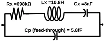
4.1 MEMS RLC (fitted) electrical model:
In this work, an electrostatic clamp-clamp beam type resonator with a measured Q of 1000 is adopted. A series RLC fitted model is constructed (Fig. 6)from the experimental measurements,which foundation has been indicated in Section 2. In this two port representation, there is no need to include a DC supply source because in calculating Rx,Lx andCx values already VDCwas included in
the value of.
Rx =698kΩ Lx =10.8H Cx =8aF
[image:4.595.326.536.112.451.2]Cp (feed-through) = 5.8fF
Figure 6. Electrical model a two port representation of the electrostatic resonator
4.2 S-parameter analysis:
The sustaining amplifier has been designed with sufficient gain to replenish resonator motional losses. In the view of the s-parameter analysis, we can estimate the net resonator loss, with the definition of ‘Forward Transmission, S21’:
|S21| 2
= Transducer gain =
source from power Available
load to delivered Power
_ _ _
_ _ _
While doing SP analysis, the source end and load end, both are terminated ideally by 50 Ω [3,6].So, forward
transmission S21 analysis data is important to estimate the
insertion loss (Fig. 7a) and the phase shift (Fig. 7b) to compensate.
(a)
[image:4.595.332.531.532.649.2](b)
Figure 7. S21 parameter in fitted model: (a) Magnitude
(b) Phase
The findings for this particular resonator (measured by Silterra, Malaysia Sdn. Bhd) are summarized in Table1.
Table 1:Resonator summary
Extracted Attributes of the MEMS Resonator
Value
Resonant frequency 17.22 MHz
Quality factor 1000
Insertion loss ~18dB
Transmission Phase 1000
4.3 Required gain calculation:
In the current case, motional resistance is Rx= 698 kΩ.
Taking into consideration the general criteria stated in Section 3.4, minimum transimpedance gainrequired is calculated as below [3]:
In ‘two port’ model of Fig.6, we find, Rx= 698 kΩ.
So,Rmotional≥ (698kΩ * 1.5) or (1.02) MΩ
Therefore,
Required “Transimpedance gain” ≥ 20 log10 (1.02 x 10 6
) or, 120.39 dB-Ω. So, in order to sustain this resonator’s
[image:4.595.86.270.560.632.2]oscillation, a gain greater than 120.4 dB-Ω is needed.
4.4 Sustaining Amplifier:
With reference to section 3, this work achieves a total gain of 122 dB-Ω with a phase shift of -700which is seemed to be sufficient (as greater than the calculated 120.39 dB-Ω) to sustain the oscillation in close loop operation. In this section, the simulation results of different amplifier stages are given through AC analysis plots.
4.4.1 TIA AC analysis:
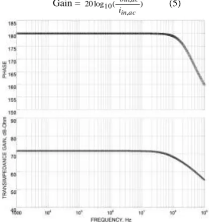
Gain and phase plots for first stage TIA of Fig. 3 are given in Fig. 8 wherethe frequencysweep is carried from 1kHz to 1 GHz range of frequencies. The gain equation is as given below:
Gain = 20log ( )
, , 10
ac in
ac out
i v
[image:5.595.323.539.66.270.2](5)
Figure 8. First stage TIA‘transimpedance’ gain and phase
As it can be seen from Fig. 8, a net 72 dB-Ω gain is achieved at this stage with a phase shift of 1820 over the bandwidth of interest ( ≥17.22MHz )
4.4.2 Intermediate Voltage amplifier AC analysis:
An AC analysis is carried for 10Hz to 20 GHz of frequency sweep for the second stage amplifier (Fig. 4) and the responses are plotted in Fig. 9. The gain equation for this voltage amplifier is given below:
Gain = 20log ( )
, , 10
ac in
ac out
v v
(6)
As it can be seen from Fig. 9 that, a net 24 dB gain is achieved at this stage with a phase shift of 50 over the bandwidth of interest ( ≥ 17.22 MHz ).
Figure 9.Second stage Intermediate voltage amplifier gain and phase
4.4.3 Cascode amplifier AC analysis:
In Fig. 10, responses are plotted by following the similar gain equation (Eqn. (6))for the third stage CA Amplifier (Fig. 5).As it can be seen from Fig. 10, a net 30 dB voltage gain is achieved with a phase shift of -2550 over the bandwidth of interest (≥17.22 MHz ).
Figure 10. Third stage Cascode voltage amplifier gain and phase
4.4.4 Complete sustaining amplifier AC analysis:
As shown in Fig. 2, the sustaining amplifier block consists of three different amplifier blocks as described in the above sections. The total open loop gain and phase for this entire block is dependent on each block’s response and is given as in Fig. 11. Here, the ‘transimpedance’ gain equation is given by:
Gain = 20log ( )
, , _ 10
ac in
ac Cascode out
i v
(7)
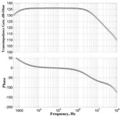
[image:5.595.67.275.252.473.2] [image:5.595.324.537.382.591.2]Figure 11.Sustaining amplifier transimpedance gain and phase plot
[image:6.595.61.279.385.566.2]As it can be seen from Fig. 11, a net 122 dB-Ω open-loop gain has been achieved with a total phase shift of -700 over the bandwidth of interest (≥17.22MHz).Now, the findings are summarized in Table 2 along with the total DC power consumption of this sustain amplifier.
Table 2:Summary of amplifier stages (gain, phase) and PDC
Amplifier stage Gain Phase (x0)
TIA 72 dB-Ω 182
Modified Cherry-Hooper
24 dB 5
Cascode Amplifier 30 dB -255
Total sustaining amplifier
122 dB-Ω -70
Total power consumption from 1.8 v, DC
6.24 mWatt
4.4.5 Transient responses over time:
Figure 12.Transient responses at different nodes:From above, Initial current signal, TIA output voltage, C-H output
voltage and Cascode output voltage
In open loop configuration, the transient responses are given in Fig. 12, where the input is a low magnitude sinusoidal current signal with 17.22 MHz frequency.
5.
Conclusion
In this work, a new sustaining amplifier is designed which is capable to compensate all the motional losses of a 17.22 MHz electrostatic MEMS resonator. This single ended operational amplifier can give a 122 dB-Ω transimpedance gain in feedback loop which satisfies the Barkhausen criteria to make the resonator’s oscillation, sustained in time. Conventional 0.18μm CMOS process was followed while designing and transient response over time, has justified the applicability of this sustaining amplifier for the reported MEMS resonator in open loop configuration.
Acknowledgment
This research is supported by the UM High Impact Research Grant UM.C/HIR/MOHE/ENG/51 from the Ministry of Higher Education, Malaysia.
References
[1] Tanaka, Shuji, Kyeongdong Park, Masayoshi Esashi. "Lithium-niobate-based surface acoustic wave oscillator directly integrated with CMOS sustaining amplifier." IEEE Trans. Ultrasonics, Ferroelectrics and Frequency Control, vol. 59, no.8, pp. 1800-1805, 2012. [2] Ferrer, E. M., Muñoz-Gamarra, J. L., Giner, J., Uranga, A.Barniol, N. “A 230MHz CMOS-MEMS bulk acoustic wave resonator”. Microelectronic Engineering, vol. 98, pp. 458-462, Jul. 2012.
[3] F. Nabki, K. Allidina, F. Ahmad, P.-V. Cicek, M. N. El-Gamal, “A Highly Integrated 1.8 GHz Frequency Synthesizer Based on a MEMS Resonator,” IEEE Journal of Solid-State Circuits, vol. 44, no. 8, pp. 2154–2168, Aug. 2009.
[4] Lopez, Joan Lluis, et al. “A CMOS–MEMS RF-Tunable Bandpass Filter Based on Two High-22-MHz Polysilicon Clamped-Clamped Beam Resonators.”
IEEEElectron Device Letters, vol.30, no.7, pp. 718-720, 2009.
[5] Pey, C., Uranga, A., Verd, J., Abadal, G., Barniol, N. “Monolithic CMOS-MEMS Oscillator in Linear Regime Operation”.
[6] H. M. Lavasani, A. K. Samarao, G. Casinovi, F.Ayazi, “A 145MHz low phase-noise capacitive silicon micromechanical oscillator,” IEEE InternationalElectron Devices Meeting, pp. 1–4, 2008. [7] J. L. Lopez, J. Verd, J. Giner, A. Uranga, G. Murillo, E.
Marigo, F. Torres, G. Abadal, N. Barniol,“High Q CMOS-MEMS resonators and its applications as RF tunable band-pass filters,” in Proc. Solid-State Sensors, Actuators and MicrosystemsConf., Denvor.CO, 2009, pp. 557–560.
![Figure 1. (a) A Clamp-clamp beam resonator (b) its motional direction (c) electrical model of it [3]](https://thumb-us.123doks.com/thumbv2/123dok_us/8646344.866344/1.595.314.549.534.697/figure-clamp-clamp-resonator-motional-direction-electrical-model.webp)