DESIGN OF M-PETFF USING LOW POWER CLOCK
DISTRIBUTION ELEMENT
A. Bakiya, M. Nithyavelam, C. Malathy and V. Balavignesh
Department of Electronics and Communication Engineering, Vel Tech Dr. RR and Dr.SR University, India E-Mail: [email protected]
ABSTRACT
An improved positive edge triggered flip flop (M-PETFF) is proposedfor Low power application with simpler structure, clock load and also compared with different flip flop designs with same size of transistor including of both input and output. The proposed work implemented in CMOS-90nm technology, gives 32% of power optimization and high performance of PDP.
Keywords: flip-flops, low power and power optimization.
1. INTRODUCTION
The millions of transistors are integrating on one chip called Soc (system on chip) technology, while the covering and cooling have a partial capacity to eradicate the overload heat. All account of these the power consumption is key part to achieve the high performance stated in ITRS 2008 and also it is listed as one of the top three challenges in VLSI system. From that Clock system is the one of the most power consuming components in a system which consists of the Flip Flops and latches [1], [2]. The 30% to 60%of total power dissipates in an entire clocking system [1]. As a result, if the power consumption of flip flop is reduced which leads major impact on the total power consumption. A huge section of the power consumption is carried by the clock drivers.
The Survey of the Flip flops stated [1]-[19], from that the single-edge triggered Flip flop are avoiding the node transition and minimize the power dissipation. But further reductions of power consumption, the double edge-triggered flip flop design are anticipated. In general the pulse triggered flip flop design, the speed is increased by minimizing the transistor during discharge path and also AND gate removed from the critical path because of reduction of complexity of the circuit and speed-up the discharge operation [3]-[7].The clock swing tree synthesis methodology is implemented with a tradition clock swing D flip-flop design is to protect the performance of IC. Another two schemes are used for design of low power FF: reduced swing and multiple-supply voltages. A Reduced swing methodology are proposed to decrease the RC delay of a long RC interconnects and power reduction [9]-[13].
Consideration of all the drawbacks, we proposed an improved positive edge triggered Flip flop (M-PETFF) design for low power VLSI systems. The design manages the propagation delay in all the node while giving the input signal and it increases the speed of data transition and also reduces the circuit complexity. Moreover this entire latch design is implemented by introducing a sleep node and sleep bar node in the circuit for extra signal driving and to reduce the leakage power.
2. PROPOSED FLIP FLOP DESIGN
A. Conventional type Flip Flop design
Figure-1. PFF design.
Figure-2. DFF design.
The Second comparative Flip flop design shows in Figure-2 [15], which is based on the frequently used static DFF. Still, pass gates with N1, N2, N5, and N6 (nMOS transistors) are used as the switches in master latches and slave latches. Accordingly, when the clock swing signal is 1, the nMOS transistor N1 and N6 can entirely switch OFF because the pass gates cannot leads voltage to the output. This problem is critical because the arriving input data signal works at FS. Therefore, A node cannot arrive at a full VDD, thus raising the outflow current and short circuit in the subsequent stages and the clock to output delay is increased. Moreover for the process variation, the pass transistors are not as much of strong. To improve this critical issue, two pMOS transistors with a pull-up network are supplementary to master and slave latches. The M node transitions to logic 0, transistor p1 switch ON. If the data signal is also at logic 0, then node A is pulled to full VDD throughout P1 and P2. During that master and slave latch are complementary to avoid leakage current and minimize power consumption.
Figure-3. M-SBFF design.
The third comparative Flip flop design shows in Figure-3 M-SBFF [19], which is used to recognize a low power and high speed FF design. The M-SBFF design reduces the load capacitance and generates the fast signal. It consists of a storage latch and inverter instead of XOR gate in order to speed up the charge and discharge of signal X. Moreover, the transistor M0 discharge the current to ground which gives the storage latch speed will be more. Additionally, two AND gates and signal X which enable the data and data bar. When CLK=0, X=1 the data and data bar are enabled and the signal X pass through
gates of M1 and M4.Consequently,the data and data bar are the function of the storage latch. The impact of gates (AND1 and AND2) does not reduce the speed of the FF design. Due to delay of the inverter the storage latch holds the preceding data when the M0 switch is closed. When M0 is open, signal X= 1 and CLK transition from 0 to 1.Finally this design provides an increased speed and reduced power consumption.
B. An improved positive edge triggering Flip flop design
From the background work the following methods P-FF, DFF and M-SBFF are used which divide dynamic node to minimize the pre-charge capacitance and consumes power in most of the conventional designs. To rectify the large power dissipation in the existing architecture, the data holding time, removal of complex logic functions and increases the Delay in the flip-flops design which turns the huge power dissipation. The drawback has been overcome by the improved Positive Edge triggering (M-PETFF) Flip flop Design.
In M-PETFF is constructed by totally 14 numbers of transistors. In existing method clock activity is based on Pulse generator and it is controlled through four inverter, AND gate, Mnx and Mn3 transistor as shown in the Figure-1[8].Apart from that it also depends on the input data which is passed on to Mn1 transistor and through Mnx transistor. Although requires M-PETFF two transistors for clock activity. Hence the proposed design has less clock activity than P-FF.
Figure-4. M-PETFF.
the flip-flop stores as 1. If CLK=0,D=0 then flip-flop stores as 0. Additionally, n8 and p6 transistors are operated with high threshold voltages to reduce the leakage power. This facilitates the power dissipation lesser then the conventional FF.
3. PERFORMANCE ANALYSIS AND RESULTS COMPARISON
CMOS-90nmtechnology is implemented by using Microwind simulation tool for the performance analysis. The supply voltage is 1 V and 2.5V for I/O supply voltage at27 degree. The Average power is found as the variation in proposed flip-flop design than the existing design. From that CMOS-90nm technology are simulated under similar conditions to extract the average power dissipation. This is calculated using
𝑝 = 𝑣𝑑𝑑. 𝑓 ∫ 𝐼𝑑𝑑𝑇 0
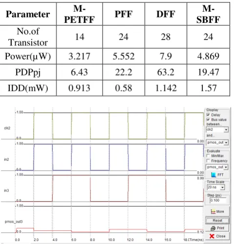
[image:3.595.312.548.96.175.2] [image:3.595.51.291.447.698.2]Where, Vdd is the supply voltage, Idd is the supply current, t is the period, and f indicates the frequency of Power dissipation. Comparison on Average power, number of transistor used, Power delay product (PDP), Maximum Idd current, and power dissipation conventional flip-flop methodologies with M-PETFF using CMOS 90nm the technology as shown in the Table-1.
Table-1. M-PETFF using CMOS 90nm technology.
Parameter
M-PETFF PFF DFF
M-SBFF No.of
Transistor 14 24 28 24 Power(µW) 3.217 5.552 7.9 4.869
PDPpj 6.43 22.2 63.2 19.47
[image:3.595.310.546.520.717.2]IDD(mW) 0.913 0.58 1.142 1.57
Figure-5. Simulation output results of M-PETFF using CMOS-90nm technology.
Figure-6. Layout diagram of M-PETFF Design.
Table-2. Power dissipation for various FF design.
Clocked latch Power dissipation (mW)
M-PETFF 0.003
P-FF 0.007
DFF 0.06
M-SBFF 0.678
The simulation results both output and layout diagram shows in Figure-5 and Figure-6, M-PETFF has the lowest power consumption than the existing FF. The power dissipation is depends on the switching activity of the transistor. For example, when clock rate is 0.5 and data for single end flip-flop (FF) is same as for the positive edge of the clock input and unequal at the negative edge. At that the data activity, DFF dissipates moderate power because the design removes the unnecessary transitions. The data activity increases further the M-SBFF design dissipates higher power. In that view M-PETFF provides better-quality performance for this data pattern shows in Table II. Moreover the maximum Idd supply current is depends of the bias condition of source, drain, gate and body of all transistor. Hence the proposed work shows the least current than all conventional type that proved in Table-1.
Figure-7. Comparison on transistors with various FF design.
proposed work shows the higher performance than the other type of FF Figure-6.Finally the results show that the conventional FF has more number of transistors compared with the PETFF shows in Figure-5.The P-FF and M-SBFF are using the 24 transistor but the average power consumed for P-FF have 7 % than the M-SBFF but in compared with DFF, 24% of power consumed in P-FF Figure-5. An improved positive edge triggered flip flop (M-PETFF) uses the 14 number of transistor that is less number of usages than the conventional type of FF design and also 32% of power only consumed in M-PETF and also higher performance for application of FF design.
Figure-8.Comparisons of average power and PDP of M-PETFF with conventional FF.
4. 5. CONCLUSIONS
In this work, a novel low power M-PETFF is proposed. An analysis of the entire work is done by Microwind tool. The proposed M-PETFF design which works efficiently in terms of switching activity of clock and data which results low power dissipation than DFF, PFF and M-SBFF. A comparison shows that lower power dissipation and Idd current along with comparable high performances by reducing number of transistor count. The layout simulation results shows reduced Power consumption and improved PDP. Furthermore by reducing the unwanted switching activity the revised structure of M-PETFF flip-flop, is efficiently utilizing complex logic in to the flip-flop.
REFERENCES
[1] H.Kawaguchi and T.Sakurai. 1998. A Reduced clock-swing flip flop (RCSFF) for 63% power reduction. IEEE J. Solid-state Circuits. 33(5): 807-811.
[2] A. Chandrakasan, W. Bowhill, and F. Fox. 2001. Design of High performance Microprocessor Circuits, 1st Ed. Piscatawa. IEEE Press.
[3] S. H. Rasouli, A. Khademzadeh, A. Afzali-Kusha and M. Nourani. 2005. Low power single- and
double-edge-triggered flip-flops for high speed applications. IEE Proc. Circuits Devices Syst. 152(2): 118-122.
[4] M.-W. Phyu, W.-L. Goh and K.-S. Yeo. 2005. A low-power static dual edgetriggered flip-flop using an output-controlled discharge configuration. in Proc. IEEE Int. Symp. Circuits Syst. pp. 2429-2432.
[5] Y.-T. Hwang, J.-F. Lin and M.-H. Sheu. 2012. Low power pulse triggered Flip-flop design with conditional pulse enhancement scheme. IEEE Trans. Very Large Scale Integration System. 20(2): 361-366.
[6] N. Nedovic, M. Aleksic, and V. G. Oklobdzija. 2002. Conditional pre-charge Techniques for power-efficient dual-edge clocking. in Proc. International Symposium of Low-Power Electron. Design. pp. 56-59.
[7] J. Tschanz, S. Narendra, Z. Chen, S. Borkar, M. Sachdev and V. De. 2001. Comparative delay and energy of single edge-triggered and dual edgetriggered pulsed flip-flops for high-performance microprocessors. In Proceeding on ISPLED. pp. 207-212.
[8] Jin-Fa Lin. 2014. Low-Power Pulse-Triggered Flip-Flop DesignBased on a Signal Feed-Through Scheme. IEEE Trans. Very Large Scale Integration system. 22(1): 181-185.
[9] E. G. Friedman. 2001. Clock distribution networks in synchronous digital integrated circuits. Proc. IEEE. 89(5): 665-692.
[10]C. Sitik, L. Filippini, E. Salman, and B. Taskin. 2014. High performance low swing clock tree synthesis with custom D flip-flop design. in Proc. IEEE Comput. Soc. Annu. Symp. VLSI. pp. 498-503.
[11]W. Liu, E. Salman, C. Sitik, and B. Taskin. 2015. Enhanced level shifterfor multi-voltage operation. in Proc. IEEE Int. Symp. Circuits Syst.pp. 1442-1445.
[12]J. Pangjun and S. S. Sapatnekar. 2002. Low-power clock distribution using multiple voltages and reduced swings. IEEE Trans. Very large Scale Integr. (VLSI) Syst. 10(3): 309-318.
[14]Weste N.H.E. 2005. CMOS VLSI design: a circuits and systems perspective. (China Machine Press, Beijing).
[15]Can Sitik, Weicheng Liu, BarisTaskinand Emre Salman. 2016. Design Methodology for Voltage-Scaled Clock Distribution Networks. 24(10): 3080-3093.
[16]Li X., Jia S., Liang X. and Wang Y. 2012. Self-blocking flip-flop design. Electron. Lett. 48(2): 82-83.
[17]Matsui M., Hara H., Uetani Y., et al. 1994. A 200
MHz 13 mm2 2-D DCT macrocell using sense-amplifying pipeline flip-flop scheme. J. Solid-State Circuits. 29(12): 1482-1490.
[18]D. Markovic, B. Nikolic and R. Brodersen. 2001. Analysis and design oflow-energy flip-flops. in Proc. Int. Symp. Low Power Electron. Des. Huntington Beach, CA, Aug. pp. 52-55.
[19]Shigematsu, S. Mutoh, Y. Matsuya, Y. Tanabe and J. Yamada. 1997. A1-V high-speed MTCMOS circuit scheme for power-down application circuits. IEEE J. Solid-State Circuits. 32(6): 861-869.