,/
, ", , '
,
v
J., /, " f " ,
"
.
/ ' , ,1 •
I ",-,
'"
",-
' " ." ,.
. "
"
'.'
'~'
". ,
,
ANALOG'-
a
DIGITAL
, "'/ :-',CONVERSION
HANDBOOK
The Digital Equipment Corporation makes no representation that the interconnection of its modular circuits in the manner described herein will not infringe on existing or future patent rights. Nor do the descriptions contained herein imply the granting of licenses to make, use, or sell equipment constructed in accordance therewith.
i I
fl
.'1 ,II \1 :! ,;1, 'I
' .. : " 'I :,];\,
"~I:" ~I q
,il
\\"
'I
' j
,
" I
I
,'i
,I '\ ,I j
'li;-"ii)'
',I",\, ((11 ' , ';,::;.. ,
I. \ , I
1'1
'I ~
I
'.I
, ",I,
I ( "
i
)
,':
ANALOG - DIGITAL
CONVERSION HANDBOOK
Barbera W. Stephenson
Copyright 1964 by Digital Equipment Corporation
PREFACE
The Analog-Digital Conversion Handbook represents the first attempt in the data process-ing industry to assemble comprehensive information on this subject in a form that makes it immediately useful to beginner or expert_ All phases of conversion are covered, from concepts to calibration. Many diagrams supplement the text; and tabular summaries of terms, methods, and performance characteristics are included for comparison and refer-ence. Circuit modules and other equipment manufactured by Digital Equipment Corpora-tion are menCorpora-tioned specifically, so after choosing the conversion method most appropriate to his needs, the reader can construct his system directly.
The use of circuit modules in constructing analog-digital converters yields several advan-tages. First, they are flexible. Converter systems have widely varying requirements, from pulse height analysis, where differential linearity is of utmost import.ance, to time-locked averaging in biomedical work, where resolution is more critical than repeatability or even accuracy. Modules permit the construction of the exact type of converter needed and, should requirements change, the same modules can be used later to build a different kind .of system.
Second, modules are economical. Aside from the interchangeability mentioned above, sav-ings are gained in the cost of construction. The typical cost of a digital-to-analog converter is about $1,000; of an analog-to-digital converter, about $2,000. If several systems are built, the cost per converter decreases since the same power supplies and mounting panels are used for the additional units. If the speed requirement is exceptionally high, costs will be higher.
A third advantage of using modules is that the completed converter need never go back to the factory for recalibration. Procedures for calibration and adjustment are included in this handbook. Recalibration can be carried out quickly and easily by the user.
Those modules designed exclusively for use in conversion systems are specified in detail in this handbook. The general purpose logic modules also needed are mentioned by name and type number. Complete specifications for these and over 200 other kinds of circuit modules and accessories are contained in the Digital Module Catalog, available at any Digital Equipment Corporation office. The catalog also contains much information helpful in designing and assembling digital systems.
CONTENTS
CHAPTER 1: BASIC ELEMENTS OF CONVERSION Introduction .... . ... .
Digital-to-Analog Conversion Analog-to-Digital Conversion
Simultaneous Method Feedback Methods ... . Counter Method ... .. Continuous Method ... . Successive Approximation Method Sample and Hold
Multiplexing. Digital-to-Analog Analog-to-Digital ....
CHAPTER 2: MEASURES OF CONVERTER PERFORMANCE Accuracy.. . ... .
Digital Error Sources ... . Analog Error Sources ... ... . ... . Differential Linearity ... .
Distribution of Error . .. . ... .
Measures of Speed .. ... ... ... ... . ... . ... . Digital-to-Analog Conversion .... .... ... ... .... ... ... ... . Analog-to-Digital Conversion ... . Selecting a Conversion Method ... .. ... . ... .
Page 1 1 2 2 3 3 4 4 5 6 6 7 9 9 10 10 11 12 12 12 15
CHAPTER 3: SPECIAL ANALOG-TO-OIGITAL CONVERSION TECHNIQUES Variations in Basic Techniques ....
Section Counter .... . Ramp Method ... .
Continuous Converters with Additional Comparators ... .
Successive Approximation Converter with Redundancy ... . ... .. Advanced Techniques. ... ... .. ... ... ... . ... . ... .
Subranging with Redundancy ... .. ... ... .. .. ... .... .... . ... . Sequential Approximation . ... ... . ... . Quantizing Encoder ... .... ... ... ... ... ... ... . ..
CHAPTER 4: TYPICAL CONVERTER LOGIC Digital-to-Analog Conversion
Analog-to-Digital Conversion Simultaneous Conversion Counter Method ... . Continuous Conversion .. .
Successive Approximation Converter
r
CHAPTER 5: BASIC CIRCUITS Divider Networks .... . ... .
Page
39
Input Impedance ... :/"'-,... ... .... ... 39
Loading the Output. .... .... ... ... ... ... ... .... . . ... ... ... ... 39
Resistor Divider Modules ... ,... ... . ... .. ... ... .. .. ... 40
Level Amplifiers ... ... ... ... ... ... ... 40
Reference Supplies ... , . 43
Comparators. ... ... ... ... ... 45
Factors Affecting Comparator Accuracy... ... ... ... ... 45
Use of the Comparator ... " ... ".... 45
Multiplexer Switches ... , ... ... ... 47
Analog Multiplex Switches ... ... ... .... ... ... ... ... 47
Use of the Type 1578 Switch ... ... ... 47
Relay Multiplexer Type 1807 ... ... ... ... ... ... 49
Digital Circuits . ... ,.. ... 50
Analog Amplifiers ... . .... ... ... ... .. ... .... 51
CHAPTER 6: INTERCONNECTION AND CALIBRATION Grounding and Shielding ... ... ... 53
Calibration ""'''''''''''''' ... ... ... ... ... 54
Equipment Needed ... ... . ... " ... .... ... 54
General Procedure ... .. ... ... 54
Divider Alignment. ... ... ... .. . .... .... ... 56
The Comparator Type 1572 ... , 58
Offset and Gain ... , ... ... ... 59
Speed Adjustments.. . ... ... ... .... ... ... ... 60
Noise and Ripple ... ... ... ... .... ... .... ... ... ... ... 60
Analog-to-Digital Adjustments .... ... 60
Digital-to-Analog Adjustments ... ... .... ... .. ... ... 61
CHAPTER 7: TESTING AN ANALOG-TO-DIGITAL CONVERTER Montonicity ... ... .. ... .. 62
Steady State Accuracy ... ... """"""""'"'''''''' ... .. 62
~~ ... . 63
Intermittent Errors ... . 63
Settling Time (Digital-to·Analog) ... '''''' ... .. 63
Response to Transients (Analog-to-Digital) .... " ... : ... .. 64
Operating Checks ... ... ... .. ... . 64
APPENDICES Appendix 1: Signed Digital Numbers ... . 66
Appendix 2: Bipolar Voltages . ... .. 67
Appendix 3: Table of Voltages ... . 69
Appendix 4: Digital Symbols and Standards . . ... .. ... .. 70 iv
.. '
[image:6.522.87.441.48.289.2]-ILLUSTRATIONS
PageFigure 1: Digital-to-Analog Conversion ... ...
r
Figure 2: Simultaneous Analog-to-Digital Converter ... 2
Figure 3: Analog-to-Digital Converter ... ... . ... ... ... 3
Figure 4: Counter Converter ... ... .. .. Figure 5: Continuous Converter .. .. ... .... ... . Figure 6: Successive Approximation Converter ... .. ... .. Figure 7: Sample and Hold ... :. ... . .. . Figure 8: Digital-to-Analog Systems ... .. Figure 9: Multiplexed Analog-to-Digital Conversion System. .. ... . Figure 10: Counter Type Analog-to-Digital Converter with Multiplexed Input .. .. Figure 11: Measures of Cumulative Error ... . Figure 12: Counter Converter ... ... ... ... .... . ... ... . ... . Figure 13: Continuous Converter ... .. Figure 14: Successive Approximation Converter ... .. ... . Figure 15: Successive Approximation Converter with Sample and Hold ... .. Figure 16: High Speed Continuous Converter ... .... ... .. ... .. Figure 17: Subranges for a Converter with Four Subranges per Step Figure 18: Subranging Converter . ... ... ... ... ... .. ... . Figure 19: Non-Synchronous Sequential Approximation. .. ... . Figure 20: Sequential Approximation (Synchronous) ... .. Figure 21: Quantizing Encoder Method .. , .. ... .. ... .. Figure 22: Digital-to-Analog Converter .... ... ... ... ... .. ... .. Figure 23: Simultanous Converter ... .. Figure 24: Typical Counter Converter ... ... ... . Figure 25: Continuous Converter with Buffered Flip-Flops ... .. ... .. Figure 26: Continuous Converter with Unbuffered Flip-Flops ... .. Figure 27: Successive Approximation Counter ... .. Figure 28: Binary Ladder . . .. . ... ... .. ... .. Figure 29: Ladder Network Specifications ... ... ... .... ... .. ... . .. Figure 30: Precision Level Amplifier Specifications ... ... .. ... . Figure 31: Reference Supply Specifications ... . Figure 32: Comparator Specifications ... ... ... .. ... . Figure 33: Multiplexer Switch Specifications... .. ... . Figure 34: Typical Amplifier Configuration for Scaling and Biasing ... .. Figure 35: Type 1751 Operational Amplifier.. . . .... .. ... . Figure 36: Divider Adjustment... .... .... ... ... .. ... .
TABLES
3 4 5 5 6 7 7 9 13 14 14 15 19 21 22 23 24 25 27 29 31 34 35 37 39 41 42 44 46 48 51 52 56 Table 1: Analog-to-Digital Conversion Techniques.. ... .... ... . ... 16Table 2: Recommended Modules for Medium Speed Digital-to-Analog Converter 28 Table 3: Recommended Modules for Simultaneous Converter up to Four Bits 30 Table 4: Counter Converter Conversion Time ... ... .... ... .. ... ... ... ... 32
Table 5: Continuous Converter Conversion Times... ... ... 36
Table 6: Successive Approximation Conversion Times ... , 38
Table 7: Inverter Amplifiers Speed and Accuracy ... . .. . .. .. 43
Table 8: Useful Logs ... ... ... ... ... .. ... . . 49
Table 9: Transition Times for Digital Modules ... .. ... ... .... .... 50
("
I
CHAPTER I
BASIC ELEMENTS OF CONVERSION
Introduction
This chapter describes the general technique used to convert, to sample and hold, and to multiplex.
For digital-to-analog conversion, just one technique is described. Though there may be some variations, the same technique is generally applicable for all digital-to-voltage or digital-to-current converters.
Analog-to-digital conversion is somewhat more complex and thus a variety of different methods is commonly used. In this chapter, the four most common methods are described. Of these, the successive approximation converter is most generally used since it provides good performance over a wide range of applications at a reasonable cost. However, if the converter is to be used only in a single application, various other methods may be preferred for better performance or lower cost.
It is suggested that this chapter be read as a brief development of the principles of con-version, rather than a delineation of specific methods. Detailed descriptions of conversion systems will be given in Chapters 3 and 4.
Digital-to-Analog Conversion
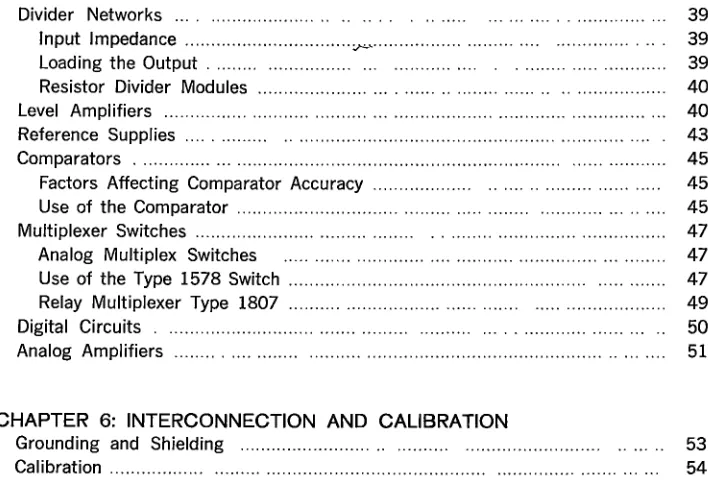
To convert from a digital number to an analog voltage, a resistive divider network is con-nected to the flip-flop register which holds the digital number (see Figure 1). The divider network is weighted so that each bit of the register will contribute to the output voltage in proportion to its value.
Figure 1 Digital·to·Analog Conversion
The digital input signal determines the analog output voltage, since the divider network is simply a passive element. However, because digital voltage levels are not usually as precise as required in an analog system, level amplifiers are placed between the flip-flops and the divider network. The amplifiers switch the divider network between ground and a
[image:9.524.162.365.456.523.2]I
I
reference voltage supplied by a precision reference supply. The output voltage range is between these two voltage levels. In Digital systems, the range is normally 0 to -10 volts. If the digital·to·analog converter is to drive long cable or a heavy load, an operational amplifier or emitter follower is usually put on the output of the circuit to lower the output resistance.
The level amplifiers, divider network, and reference supply shown in Figure 1 are basic to a digital-to-analog converter and are described under those headings in Chapter 5.
Analog-to-Digital Conversion
The basis of analog-to-digital conversion is the comparator circuit. This circuit compares an unknown voltage with a reference voltage and indicates which of the two is larger.
SIMULTANEOUS METHOD
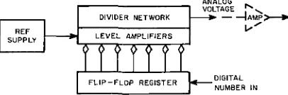
Figure 2 shows how a simple simultaneous analog-to-digital converter can be built using several comparator circuits. Each comparator has a reference input signal. The other input terminal of the comparators is driven by the unknown input analog signal, which is between
o
and V volts. The comparator is called "ON" if the analog input is larger than therefer-ence input. Then, if none of the comparators are on, the anaJog input must be less than
~ . If C-l is on, and C-2 and C-3 are off, the input must be between ~ and
T .
Similarly,if C-l and C-2 are on, and C-3 off the voltage is between
T
and3: ;
and if all thecompara-tors are on, the voltage is greater than
3: .
ANALOG INPUT IS BETWEEN OANO v VOLTS
COMPARATOR OUTPUTS
Figure 2 Simultaneous Analog-to·Digital Converter c, C2
off off on off on on on on
C, Input Voltage off
o
to V/4 off V/4 to V/2 off V/2 to 3V/4 on 3V/4 to VHere, the voltage range is divided into four parts, which can be coded to give two binary bits of information. Seven comparators would give three bits of binary information. Fifteen comparators would give four bits. In general, 2N-l comparators will give N bits of binary information.
[image:10.521.170.413.373.519.2], I
The simultaneous method is extremely fast for small resolution systems. For large resolu-tion systems (a large number of bits), this method requires so many comparators that it becomes unwieldly and prohibitively costly.
FEEDBACK METHODS
If the reference voltage were variable, only one comparator would be needed. Each of the possible reference voltages could be applied in turn to determine when the reference and the input were equal. But a digitally controlled variable reference is simply a digital-to-ana-log converter. Thus the generalized anadigital-to-ana-log-to-digital converter shown in Figure 3 is actually a closed-loop feedback system. The main components are the same as a digital-to-analog converter plus the comparator and some control logic. With a digital number in the DAC (digital-to-analog converter) the comparator indicates whether the corresponding voltage is larger or smaller than the input. With this information, the digital number is modified and compared again.
ANALOG INPUT , - - - I
I I
I
I
,J!...Jc::;--11
1
DIVIDER NETWORKI
I
I
I
I
I
L _
~IGITA=-=-T~ANALr::. C~VERT~_-.J
Figure 3 Analog-to·Digital Converter Incorporating a Digital·to-Analog Converter
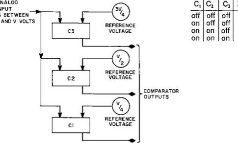
COUNTER METHOD
Numerous methods may be used for controlling the conversion. The simplest way is to start at zero and count until the DAC output equals or exceeds the analog input.
Figure 4 shows a converter in which the DAC register is a counter, and a pulse source has been added. The gate stops pulses from entering the counter when the comparator indi-cates that the conversion is complete.
ANALOG INPUT
Figure 4 Counter Converter
[image:11.519.155.372.255.362.2] [image:11.519.139.386.506.597.2]F
I
The counter method is good for high resolution systems: As the number of bits is in-creased, very little additional circuitry is needed. Multiple inputs can easily be converted simultaneously (as described under Multiplexing later in this chapter). However, conversion time increases rapidly with the number of bits, since an N-bit converter must allow time
for 2N counts to accumulate. The average conversion time will, of course, be half this
number.
CONTINUOUS METHOD
A slight modification of the counter method is to replace the simple counter with an up-down counter as in Figure 5. In this case, once the proper digital representation has been found, the converter can continuously follow the analog voltage, thus providing readout at an extremely rapid rate. This method, called continuous conversion, is particularly useful when a single channel of information is to be converted. The converter starts running, and the digital equivalent of the input voltage can be sampled at any time.
ANALOG INPUT
Figure 5 Continuous Converter
The continuous method is less effective for multiple inputs or for inputs that change faster than the converter can change. Each time the input makes a large change, the converter
may require as many as 2N steps to catch up. However, if a rapid rate of change is
neces-sary, extra comparators may be added so that the up-down counter can count in units of 2, 3, 4.or more (see Chapter 3).
SUCCESSIVE APPROXIMATION METHOD
For higher speed conversion of many channels, toe successive approximation converter is used. This method requires only one step per bit to convert any number. The successive approximation analog-to-digital converter operates by repeatedly dividing the voltage range in half as follows:
.______111
<0:::::::::::::
111~110~ 110
,,/" 1 0 k:::::::,:: 1 01
100 100
~
010<011~011
~0104
[image:12.521.143.382.262.357.2]Thus, the system first tries 100, or half scale. Next it tries either quarter scale (010) or three-fourths scale (110) depending on whether the first approximation was too large or too small. After three approximations, a 3·bit digital number is resolved.
Successive approximation is a little more elaborate than the previous methods since it requires a control register to gate pulses to the first bit, then the second bit, and so on. However, the additional cost is small and the converter handles all types of signals about equally fast.
ANALOG INPUT
DIVIDER NETWORK
CONTROL REGISTER
Figure 6 Successive Approximation Converter
The successive approximation method is good for general use. It handles many continuous and discontinuous signals and large and small resolution conversions at a moderate speed and moderate cost.
Sample and Hold
I
A sample and hold circuit is used in an analog·to·digital converter whenever it is desirable to make a measurement on a signal and to know precisely when the input signal cor· responded to the results of the measurement. It is also used to increase the duration of a signal.
The sample and hold circuit can be represented as shown in Figure 7. When the switch is closed, the capacitor is charged to the value of the input signal; then it follows the input. When the switch is opened, the capacitor holds the same voltage that it had at the instant the switch was opened.
IN~ _ _ ..,.--_ _ OUTPUT
Ie
T
Figure 7 Sample and Hold
It is possible to build a sample and hold circuit just as shown here. Often, the same circuit is used with a high gain amplifier to increase the driving current available into the capacitor
[image:13.521.154.361.168.264.2]or to isolate the capacitor from an external load on the output. In some cases, this sample and hold is made entirely differently; but from a logical point of view, it acts as the ideal component shown.
The acquisition time of a sample and hold is the time required for the capacitor to charge up to the value of the input signal after the switch is first shorted. The aperture time (see definition, Chapter 2) is the time required for the switch to change state and the uncer· tainty in the time that this change of state occurs. The holding time is the length of time the circuit can hold a charge without dropping more than a specified percentage of its initial value.
Multiplexing
Often it is desirable to multiplex a number of analog channels into a single digital channel or conversely a single digital channel into a number of analog channels. Multiplexing can take place in the digital realm, the analog realm, or in the conversion process.
DIGITAL-TO-ANALOG
In digital· to-analog conversion, a common problem is to take digital information which is arriving sequentially from one device, such as a digital computer, and to distribute this in-formation to a number of analog devices. Usually it is necessary to hold the inin-formation on the analog channel even when it is not being addressed from the digital device. There are two ways to multiplex. A separate digital-to-analog converter may be used for each channel as shown in Figure 8.
PULSES READ INTO SELECTED CHANNELS
Figure 8 Digital·to·Analog Systems
ANALOG OUTPUTS
In this case, the storage device is the digital buffer associated with the converter. Or, a single digital-to-analog converter may be used, together with a set of multiplexing switches and a sample and hold circuit on each analog channel. The cost of the first method is
[image:14.519.167.369.372.543.2]I
I
)
.
I
\slightly more than the cost of the second method, but it has the advantage that the infor· mation can be held on the analog channel for an indefinite period of time without deteriora· ting; whereas with the multiple sample and hold technique, it is necessary to renew the signal on the sample and hold at periodic intervals.
ANAlOG-TO-DIGITAL
In analog·to·digital conversion, it is more common to multiplex the inputs in the analog realm. Here switches, either relays or solid state, are used to connect the inputs to a com· mon bus. This bus goes into a single analog·to·digital converter which is used for all chan· nels (see Figure 9). If simultaneous time samples from all channels are required, a sample and hold circuit can be used ahead of each multiplexer switch. In this way, all channels would be sampled simultaneously and then switched to the converter sequentially. The multiplex switches and sample and holds will introduce some error into the system. How· ever, it is usually less expensive to go to higher quality sample and hold and multiplex circuits than add extra converters.
~
~
~---+---l
DIGITAL OUTPUTS
~
ANALOG INPUTS
~ ~----~
~
Figure 9 Multiplexed Analog-to-Digital Conversion System
In a simple analog-to-digital converter with a single comparator circuit, it is also possible to multiplex by using a separate comparator for each analog channel. One input of each comparator is tied to the voltage generating device in the converter. The other inputs are tied to the separate analog channels. The comparator to be used can be selected digitally. This method is particularly good when a small number of channels is to be multiplexed since it is quite simple and requires little additional control. For a large number of chan· nels, separate multiplexer switches are usually less expensive and more accurate as they do not put any load on the voltage generating device of the converter.
ANALOG INPUTS
.
LADDER NETWORKS LEVEL AMPLIFIERS
COUNTER
Figure 10 Counter Type Analog-to-Digital Converter with Multiplexed Input
7
[image:15.519.160.364.262.366.2] [image:15.519.144.372.496.587.2]The comparator multiplexing technique is particularly useful with the counter type analog-to-digital converter. This technique is shown in Figure 10. Several comparators are at-tached to one converter. The counter is cleared; then count pulses are applied. When one of the comparators signals that the digital-to-analog output is greater than the input volt-age on that channel, the contents of the counter are read out. Counting is then resumed until the next signal is received.
CHAPTER 2
MEASURES OF CONVERTER PERFORMANCE
Accuracy
Since the end result of conversion is the representation of a given value in different
terms, it is important to know how accurate the representation is. In systems where accuracy requirements are not too stringent, say in the order of 1 percent, an overall accuracy specification is usually sufficient. In cases where the desired accuracy is 0.1 percent or greater, it is necessary to isolate the various sources of error; and since a
converter is a hybrid device, both digital and analog sources must be taken into account.
In high accuracy systems particularly, accuracy figures given in the general
specifica-tions may not include isolated sources of error, e.g., noise. Thus, it is important to know the various types of errors, their causes, how they are measured and specified, and when they are important. Figure 11 shows a breakdown of various types of errors.
Figure 11 Measures of Cumulative Error
DIGITAL ERROR SOURCES
When a continuous signal is quantized, there is an error which is equal in magnitude to
the smallest quantum. For a linear converter, the smallest quantum is the least significant
bit. In most converters the quantization error is centered so that it is equal to -+-% the
least significant bit, written as -+-1j2 LSB.
In a continuous converter or digital voltmeter, accuracy may not be as important as
avoiding chatter. That is, if the input is right on the dividing line between two tion states, the output should not oscillate. If hysteresis is introduced so that the
quantiza-tion error is just under -+-1 LSB, then oscillations will normally be avoided and the
accuracy will not be greatly impaired.
[image:17.520.117.398.287.410.2]The digital-to-analog converter reproduces exactly all the digital input information which it accepts_ Hence digital error is not included in its accuracy specifications_ However, if the input has more bits than the converter, there will be a quantization error in the
readin process which should be taken into account If desired, a 1/2 LSB offset can be
built into the converter so that the readin will round off, rather than truncate, more precise digital information_
ANALOG ERROR SOURCES
The dc accuracy of the converter (or switching point accuracy) depends on the offset, the gain calibration, and the linearity_ Nonlinearities are due to the variation in gain (or common mode effect) in going from the smallest input to the largest input Some of these will be long-term, because of the common mode effect of the comparator circuit in the analog-to-digital converter, for example_ Some will be shorter term, because of dis-continuities in the divider network or insufficient settling time of the comparator. The offset and the gain can be adjusted in the calibration until their effects are essentially negligible_
The measurement of analog error in a digital-to-analog converter is easily made by put-ting in a digital number (the same word length as the converter) and observing the output In an analog-to-digital converter, the analog error is difficult to locate since the
quantiza-tion error is always present However, the point where the output oscillates approximately
equally between two neighboring digital numbers is fairly well-defined_ This point, called the switching point, can be measured and compared with the theoretical value_
The ripple on the reference supply and other sources of noise are often measured sep-arately since one or the other can sometimes be neglected in the final result The two can be separated by measuring the ripple in the reference supply and subtracting it from the measured noise, or by running the input source in the converter from the same reference, thereby giving a direct measurement of all noise sources except the reference supply ripple_ In a digital-to-analog converter the noise and ripple can be measured by
observing the output with a scope. In an analog converter they can be measured by
observing the input range which causes the output to oscillate between two states.
DIFFERENTIAL LINEARITY
Differential linearity is the variation in the size of the required voltage change that causes
an analog-to-digital converter to go from one switching point to another. That is, it is the variation in the size of the states and is generally quoted as a percent of the size
of the states. It is a part of the overall linearity discussed above, but deserves special
mention because of its importance when an analog-to-digital converter is being used in histogram applications. For example, when plotting the number of inputs versus the digital state, if one of the states is twice as big as its neighbor, it will tend to accumulate
twice as many counts. Naturally, a very misleading output results.
Differential linearity is one of the few accuracy characteristics which is affected by the conversion technique. The differential linearity tends to be best when the converter goes
through all the states sequentially as in the counter type converter described in Chapter 1 or the ramp variation described in Chapter 3. In an approximation converter, such as the successive approximation type, the large transients which result in going from, say, half scale to quarter scale require a long time to settle down, and any hysteresis in the com-parator circuit causes relatively large variations in the state size. However, the differential linearity of an approximation converter can be improved by running it at very low speed. Differential linearity is also affected by variations in the divider networks (although they are relatively small). It can be avoided by using a ramp converter.
The shorter the converter word length, of course, the better the differential linearity will tend to be. However, this gain may well be compromised, since small resolution could result in the loss or the smoothing of very sharp peaks in the histogram.
Techniques commonly used to overcome difficulties with differential linearity are: chang-ing the offset on the converter (or equivalently the bias on the input signal) and changchang-ing the word length of the converter. Switches can be mounted on the converter for this
purpose, or the change can be made programmable so that the controlling device can
make the change automatically.
DISTRIBUTION OF ERROR
How much of the total error should be in the digital circuitry and how much in the analog portion? For converters in the range of up to 10 or 11 bits, the digital error generally
accounts for about 13 to 1/2 of the total. Thus, a typical lO-bit system would have a
quanti-zation error of -+-1f2 LSB and an analog error of -+-1
%.
If the accuracy requirement is low, the word length may be the major source of error. The total error may then be treated simply as round-off. If the accuracy requirements are stringent, it is desirable to minimize all sources of error, analog and digital. The digital error is quite simple to minimize by extending the number of bits within practical limits. A converter with an overall error of 0.1 % and a word length of 20 bits would be unjustified, as for all intents and purposes the least significant bit could have been gen-erated by a random number generator.
Requiring monotonicity is one way to assure that all the bits are meaningful. This means that all states must exist and they must be in the correct order. In terms of converter operation, as the number going into the digital-to-analog converter is increased, the output voltage must also increase; it should never dip back down at any point. Similarly, if the input voltage to an analog-to-digital converter is increased, the digital output should stay at the same value or increase and should not skip over any states.
The converter is most likely to lose monotonicity when switching between digital states such as 0111 and 1000. If the weighting of the bits is not quite correct, in a digital-to-analog converter the higher state might correspond to a lower voltage, and in the digital-to- analog-to-digital converter the output might jump directly from 0110 to 1000.
Measures of Speed
DIGITAL-TO-ANALOG CONVERSION
The maximum conversion rate is theoretically limited only by the minimum time between readins to the converter flip-flops, and can easily be as high as 10 megacycles. However, such a figure may be misleading. The desired ratio of settling time to non-settling time usually determines the maximum usable conversion rate.
The settling time of a converter is measured from the time the digital readin is performed to the time when the analog output has settled to within the specified limits of accuracy. How the output approaches its final value depends on the output circuit, as discussed below.
The divider output will have high frequency transients before it begins to settle. If the output is going to a low frequency device, the transients can be ignored. In some applica-tions, it is more desirable to smooth the transition between states than to minimize the total time, in which case the oscillations can be damped with the capacitor or a low pass filter.
If the output is from an amplifier circuit, the settling time will be determined by the maxi-mum rate of change of the amplifier. Thus, the first readin may take longer to settle than subsequent read ins, which usually do not change the converter by such a percentage of the full scale.
ANALOG-TO-DIGITAL CONVERSION
Conversion time is measured from when a request is given to when a digital output is available. In converters like the successive approximation type, where all conversions are completely independent, time must be allowed for completion of entire steps in the con-version process. In the continuous converter, the concon-version time is usually just that time required to synchronize the request and get the number.
The conversion rate is usually the inverse of the conversion time. In some systems, an amplifier or comparator recovery time is required between conversions; thus the rate is lower. However, comparators manufactured by Digital Equipment Corporation do not have a recovery time. The conversion rate will also be slower if logical operations must be carried out between conversions. In some cases, such as the counter converter performing a number of simultaneous conversions or the synchronous sequential converter, the con-version rate is actually faster than the inverse of the concon-version time.
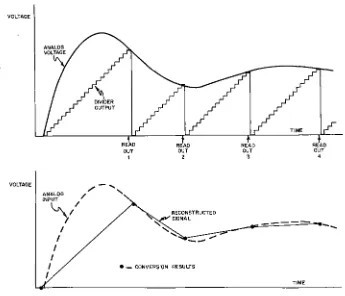
If the input signal is changing with respect to time, it is very important to know when the signal had the value given by the output. The uncertainty in this time measure is called the aperture time (sometimes also called window or sample time). The size of the aperture and the time when the aperture occurs vary depending on the conversion method.
Figures 12 through 15 illustrate how the aperture varies with different conversion tech-niques. In each case, the upper portion of the figure shows how the converter arrives at an output. The lower portion of each figure shows how the input might be reconstructed from the Digital data.
VOLTAGE VOLTAGE READ OUT t READ OUT 2 READ OUT 3 READ OUT 4 / -...
ANALOG / " INPUT
~/
1 I I I I I I RECONSTRUCTED SIGNAL• = CONVERSION RESULTS
--~~-==-~~---~~--TIME
Figure 12 Counter Converter
In the counter converter (Figure 12) the aperture occurs at the end of the conversion. This is not constant with respect to the beginning of the conversion, but it may be calcu-lated from the digital output.
For the continuous converter (Figure 13) the aperture is the time for the last step. Here the assumption is made that the input signal does not change more than -+-1 LSB between conversion steps. To meet this requirement, the maximum rate of change of the input voltage must not exceed the maximum rate of change of the converter. This is V,e./2NL"iT where V reference is the full scale voltage, N is the number of bits, and L"iT is the time per step. The maximum rate of change of the sine wave is 27rVpf, or 7rVppf. Thus, if the converter is to follow the input, the maximum frequency components in the input must satisfy the following equation:
7rVppf=V,e./2NL"i T
and if the peak-to-peak voltage is assumed equal to the converter reference, then the maxi-mum frequency is:
[image:21.520.70.415.53.349.2]VOLTAGE
TIME
VOLTAGE
,...-
...
,
ANALOG / ... INPUT ... / ' ",.
~ "
I '\, .. ..-,"'" .-,a.~ ~ .-:: .-:-:.-r-..
""'-/
''l-... ,.,. .
.-I . ' \ .-:-:~.~.~
I . . . RECONSTRUCTED
I SIGNAL
I EACH DOT INDICATES A READ OUT
I ...
TIME
Figure 13 Continuous Converter
VOLTAGE
READ READ READ READ READ READ READ READ READ READ READ READ READ OUT OUT OUT OUT OUT OUT OUT OUT OUT OUT OUT OUT OUT I 2 3 4 5 6 7 8 9 10 11 12 13
VOLTAGE
RECONSTRUCTED SIGNAL
...
-.,....
EACH HORIZONTAL LINE INDICATES THE DIGITAL READOUT AND APERTURE
TIME
Figure 14 Successive Approximation Converter
14
[image:22.517.52.416.56.593.2] [image:22.517.70.418.332.585.2]For a successive approximation converter (Figure 14) the digital output corresponds to
some value the analog input had during the conversion. Thus, the aperture is equal to the
total conversion time. Aperture time of the successive approximation converter can be_
reduced by using the redundancy techniques outlined in Chapter 3 or by using a sample and hold circuit. The sample and hold is illustrated in Figure 15.
VOLTAGE
VOLTAGE
RECONSTRUCTED SIGNAL
• =CONVERSION READOUT
Figure 15 Successive Approximation Converter with Sample and Hold
SELECTING A CONVERSION METHOD
Chapters 1 and 2 have summarized several methods of conversion and the performance
characteristics that may be expected from them. These criteria for choosing a specific
conversion method are condensed in Table 1. The table is organized like the handbook
with applicable chapters called out for quick reference to detailed descriptions of the methods.
The decision to choose one converter over another is principally a matter of speed,
aper-ture, cost, and whether multiplexing or a single continuous input is to be used. Exact conversion times, aperture times, and cost depend on the number of bits, type of circuitry,
[image:23.522.75.419.166.418.2]TABLE 1 ANALOG TO DIGITAL CONVERSION TECHNIQUES
-0'" Q) .... x'"
* *
Q)o.
Q) Q)
....
- < : a
0 . - E .S~
* * ~
~V1
~-- Q) Q)u Q)
-'"
1-'"' EU' E<lJ E'" a <:Q)
'"'
<:Ul Q) -Q) ._ Ul t=2", 0 ' " Q2, I-Ul 1-3 '-.~ _ :l. Q) :l.
....
".~~ ~Ul ~~ Q) <:e <lJ
0 .... ~'"
.... <:
Q) '" Q)~ "'Ul
"'
....
"''''
>1;)8
>:t:: E:CO t."t: tm t l t :;::;"'
.... <:co Q)CO <lJ <: Q)_
'"
Method COo Q)~ Oll) a 0 .... 0 0 <!ll) 0. <! ... 0.0 O<! 0 0 . Q:O Q)O Remarks BASIC METHODS (Chap. 1 & 4)
Simultaneous Both Not Applicable Yes Depends on Excellent for low resolution systems - operates resolution In about 100 nanoseconds
Counter M 24 avo 1792 avo 1.5 3.5 No Low Allows many conversions simultaneously
Continuous Extremely high speed for continuous input but falls
Continuous Input C 1.5 2 1.5 2 Yes Low to behind on sharp rate of change Discontinuous Input C 24 avo 1024 avo Yes Medium
Successive Approximation M 7.5 36 7.5 36 Yes Medium General purpose - good speed/dollar
0; VARIATIONS ON BASIC METHODS (Chap. 3)
Ramp M 16 avo 512 avo 1 1 No Depends on Good differential linearity - low" cost for low resolution resolution systems
Section Counter M 18 112·224 1.5 3.5 No Low to Used with digital voltmeter medium
Continuous with add. compo
Continuous Input C 1.5 2 1.5 2 Yes Medium to Similar to continuous but has faster responses to Discontinuous Input C 6·12 avo 32·512 avo 1.5 2 Yes High discontinuous or high speed signals
Successive Approximation M 9 27 1.5 3 Yes Medium to Good speed per dollar In high resolution systems.
with Redundancy High Small aperture, good differentiallineanty
- - - . - - - . _
-ADVANCED (Chap. 3)
Subranging M 3-4 10·20 3·4 10·20 Yes High Excellent for 5 to 8 bits Subranging with Redundancy M 2.5 6·9 1.5 3 .Yes High Excellent for 7 bits or more
Seq. Approx. (Non·Synchronous) M 7.5 25 Yes High May make errors. Requires sample and hold Seq. Approx. (Synch ronous) C 1.5/9t 1.5 Yes High tTime between conversions/total time
Quantizing Excellent for both multiplexed and continuous in·
[image:24.687.45.631.60.445.2]and variations in system design. The speeds given in the table were derived assuming that the system was designed for maximum speed per dollar. Actual speeds will usually be within a factor of 2 for basic conversion methods and within a factor of 5 for the others.
The basic conversion methods, as described in Chapters 1 and 4, will satisfy most require-ments. If Table 1 confirms the choice of one of the basic methods, the reader can go directly to Chapter 4 for specific information on the equipment required. The other methods are variations of basic methods and advanced techniques primarily for increased speed. They are described in general terms in Chapter 3.
CHAPTER 3
SPECIAL ANALOG-TO-DIGITAL
CONVERSION TECHNIQUES
The analog-to-digital conversion techniques described in Chapter 1 are the most com-monly used methods but not necessarily the only ones_ There is an extremely large variety of techniques, not all of which have been investigated_ Some of the other methods are described in the following section.
Variations In Basic Techniques
SECTION COUNTER
The counter converter is a simple technique for performing conversions. However, if the
digital word becomes long, the 2N steps required to complete the conversion may be
too many.
One way to decrease the time at a minimum of cost is to divide the counter into sections. For example, a lO-bit converter could be divided into 2 sections of 5 bits each. At the beginning of the conversion the least significant counter is set to all ones and counts are inserted into the most significant counter until the comparator idicates that the input has been exceeded. The least significant counter is cleared and counted up until the correct value is reached. The maximum number of steps required to complete a conversion is
25 for the most significant counter and 25 for the least significant counter, giving a total
of 26 steps. This is a maximum of 64 counts versus 1024 counts for the standard
coun-ter convercoun-ter.
Other types of section counters might use more parts and operate by counting one counter up and the next down. The total conversion time, of course, depends on the number of sections.
The section counter technique is frequently used in digital voltmeters where the output is to be in decimal: Each section of the section counter thus represents one decimal digit.
RAMP METHOD
In the counter converter, each count input is increasing the voltage out of the DAC by one step, effectively generating a ramp out of the DAC. Thus the level amplifiers, refer-ence supply, and divider network could be replaced by an external ramp generator circuit. If accuracy is not too important, the ramp can be made by charging a capacitor with a current source and using the linear part of the exponential. In higher resolution converters, the ramp might be made by using the operational amplifier as an integrator.
The ramp technique is somewhat faster than the counter technique because carry and DAC set up time is not required before gating the next count pulse. The differential
ity, over a short span of a ramp converter, is bound to be fairly good, since the ramp is a continuous signal. Although there may be some noise, the general slope will not change significantly over a short span.
Both the ramp method and the counter technique approach the final value in small steps and from one direction only. This puts considerably less strain on the comparator circuit than a technique such as subranging or successive approximation where the comparator is receiving large input voltage changes in different directions and being asked to resolve small differences. In general, all smooth conversion techniques (the counter, ramp, and continuous converters) generally operate at a considerably faster time-per-step and produce better differential linearity than the approximation methods (subranging, succes-sive approximation, sequential approximation, etc.).
CONTINUOUS CONVERTERS WITH ADDITIONAL COMPARATORS
A continuous converter is an extremely fast and relatively inexpensive device for follow-ing a continuous signal. However sometimes the input rate of change exceeds that of the converter. To close this gap determine if the differential error exceeds a specified amount and add or subtract a correction count in a more significant bit. For example, a small amount of logic added to a lO-bit continuous converter could measure large differ-ences between the input and the contents of the converter. If the difference is more than +8 counts, it adds a count in the third flip-flop from the least significant end. If the'
ClVIDER NETWORK
ANALOG INPUT
TIMING
a
CONTROL
Figure 16 High Speed Continuous Converter
[image:27.518.170.354.324.584.2]difference is more negative than -8 counts, it subtracts a count from this stage. Thus the converter operates on high frequency signals with reduced accuracy and on low frequency signals with the full accuracy.
A continuous converter with additional comparators is shown in Figure 16. Two com· parators and additional gating and synchronizing logic have been added to a basic con· tinuous converter.
SUCCESSIVE APPROXIMATION CONVERTER WITH REDUNDANCY
Redundancy is useful where high resolution and high speed are both required. It can also be used to improve differential linearity and aperture.
The successive approximation converter is extremely efficient; but, since the results of each step are irrevocable, each step must be allowed to settle to within the total system accuracy. For high resolution systems, the settling time can be quite long. With redun· dancy, the first steps are done with a limited accuracy; then a correction step is inserted to improve the accuracy. Only the correction step and the following steps need to settle to
final accuracy. Steps before correction need only settle within +-1/2 of the correction amount.
The correction can be implemented by adding or subtracting one bit, as in a continuous converter. If the steps preceding the correction are offset, only add circuitry is necessary. For fastest operation, a special divider with redundant inputs can be used so that the addition can be done without generating carries. The digital summing can be done in an output buffer where the carries will not interfere with the analog· to-digital feedback loop.
The correction step can also be used to compensate for changes in the input analog signal during earlier steps, thereby reducing the aperture. It also improves the differential linearity of the converter since a large part of the variation in state size is due to the large transients during the early conversion steps.
Advanced Techniques
SUBRANGING
This method is very good for converting a large number of input channels since the conversion begins without assuming anything regarding the previous state of the input. It also converts quite rapidly and allows a trade-off between cost and complexity and speed. Thus, if extremely high speed is required, numerous comparators are used and not many steps are required. In the case where less speed is required, perhaps only one comparator circuit would be used.
The subranging method operates by dividing the total input signal range by the number of subranges, selecting the appropriate subrange and then dividing this into subranges as before, repeating until the desired resolution is achieved.
Figure 17 shows how subranging works. At the start of the conversion, the only informa-tion available about the input signal is that it lies somewhere in the range of zero to the
full scale voltage, VFS ' The first step of the conversion divides the full scale voltage into
subranges, in this case four. Simultaneously, comparisons are made between the input
voltage and the three subrange boundaries, V" V2 , and V,. It can be determined whether
the input voltage is higher than or lower than each of these boundaries. If the input signal is lower than all of the boundaries, it must fall in the lowest range. If it is higher
than V, but lower than V2 and V" it must fall in the next to the lowest range, and so forth.
Once this information is determined, the selected subrange can be divided into four more subranges and the process repeated.
V~
V 2
v,
o
START STEP I STEP 2
Figure 17 Subranges for a Converter with Four Subranges Per Step
If there are M ranges per step and S steps, the total resolution of this conversion will
be
(*
)5. For example, a 12-bit system requiring a total resolution ofd%
could beimplemented in 12 steps [
<+)'2
=
. ] ,
in six steps [<+)6
=
4d96 ], in foursteps [ (+)4
=
40~6 ], or in three steps [ (*)3=
41k ].
The step resolution doesnot have to be an integer power of two. However, except in a binary coded decimal system where it is useful to make M equal to 10, the saving in control circuitry is usually suffi-cient to justify increasing the step resolution to the next power of 2.
Figure 18 shows a subranging converter. Here two digital-to-analog converters and a number of comparators are referenced at equally spaced intervals in the range between the value of the two converters. The technique is similar to the simultaneous method. The system starts with the lower DAC (digital-to-analog converter) at zero, the upper one at the maximum voltage. The output of the comparators indicates which range
con-tains the input, say between the reference applied at CK and the reference applied at
CK+I • Then the reference voltage from CK is applied to the lower DAC, and the reference
voltage that was at CK+I is applied to the upper DAC. A new, smaller set of ranges is
pro-duced. The process is then repeated.
[image:29.518.159.362.162.309.2]ANALOG INPUT R R R R R R
GATES a LEVEL AMPLIFIERS
R DIVIDER
Figure 18 Subranging Converter
TIMING
a
CONTROL
If the number of subranges obtained in a single step is equal to the total system resolution, this method becomes the simultaneous method described in the introduction. If the number of subranges per step is reduced to two, this method becomes the successive approxima-tion conversion.
SUBRANGING WITH REDUNDANCY
Redundancy, as described for the successive approximation converter, can be applied in the same manner to a subranging converter. It is particularly useful here as the capacitance of many comparators in parallel causes the settling time to be quite long.
SEQUENTIAL APPROXIMATION
Sequential approximation, also called parallel approximation, uses a separate analog-to-digital converter for each binary bit of information to be obtained. There are two methods of operation, synchronous and non-synchronous.
Figure 19 shows how the non-synchronous type operates. In one example shown at the top of the figure, the analog input comes into a comparator which compares the input with half scale. If the input is larger, the comparator applies a voltage to the most signifi-cant bit of each of the DAC circuits down the line. As soon as the first comparator has
[image:30.516.158.363.55.330.2]settled, the second comparator can start to make its decision. Speed is gained because there is no flip·flop delay in this system. But more important, most comparators will make decisions relatively quickly, since the analog input cannot be very close to the boundaries of more than two subranges (the last one and one other). Thus, the average amount of time required per decision is considerably less than the maximum. In a clocked system, the maximum required time must be allowed for each step. Here, only the average time is allowed.
ANALOG
-I"j-L
__
-.J
INPUTREF
ANALOG_""_~ _ _
---1
INPUTL - - - _ F L A G
k - - - - ' - - - . DIGITAL OUTPUT
FLAG
t - - - + DIGITAL OUTPUT
Figure 19 Non·synchronous Sequential Approximation
[image:31.516.109.432.145.599.2]l
The converter shown at the lower half of Figure 19 is ,quite similar except that the individual DAC networks are replaced by operational amplifiers. The analog input goes to the first comparator. If the input is above half· scale, the comparator produces a voltage corresponding to half scale. This is subtracted from the input signal, and the result is multiplied by two and passed on to the next comparator.
In both examples, speed is gained by the fact that full settling time is not needed by those comparators which are not making a critical decision. On the other hand, some difficulties are encountered if the input signal should change slightly before the digital readout has occurred. One of the comparators may change value, but the results may not carry to the end of the chain before readout. Thus, the comparator should have built-in hysteresis so that small noise spikes will not cause an error, and the digital output should always be read into a buffer and double checked with the input.
In synchronous sequential approximation, the time required to perform a complete con-version is essentially the same as in a successive approximation converter; however, the conversion rate is much faster. Erroneous readout is eliminated, since the converter is buffered and synchronous. This type of converter is particularly useful for systems with a single input.
The synchronous or clocked type sequential approximation converter also uses one converter per bit. It differs from the non-synchronous type because there is a delay line between each converter (see Figure 20). The analog information arrives at the first comparator, which makes a decision and stores the information in a shift register for use by later converters. By the time the second converter is set up and ready to make a decision, the same analog information is just arriving at the second comparator. This converter decides on the second bit of the output word, based on exactly the same analog voltage as was at the first converter when the first bit decision was made. This process is continued for however many bits are necessary.
(
ANALOG INPUT+
SR2 SRIDIGITAL OUTPUT
-')
SRI -
SRo-Figure 20 Sequential Approximation (Synchronous)
[image:32.515.148.346.401.574.2]QUANTIZING ENCODER
The quantizing encoder was developed by Dr. Jerome Cox and Donald Glaser at the Central Institute for the Deaf. It is the most general purpose, high speed converter because it is fast for both continuous and multiplexed inputs.
The quantizing encoder uses one digital-to-analog converter, a number of amplifiers, and a number of comparators. It examines the difference between the input voltage and the DAC output, quantizes the difference to the nearest power of 2, and adds or sub-tracts this from the DAC. Thus, the quantizing encoder can follow a continuous signal, staying within one bit of the correct value for low frequencies. For high frequencies, it will always be within the nearest possible power of 2 of the correct answer. (Thus, if the input signal should suddenly change, the quantizing encoder will make a similar jump corresponding to the nearest power of 2 change, while the standard continuous converter could increase by only one count.)
For multiplexed input, the quantizing encoder will operate similar to a successive approxi-mation converter but twice as fast. It requires only one step for each two binary bits (or fraction thereof). In addition, since it includes a self-correcting ability, the time per step can be quite fast.
Figure 21 shows how the quantizing encoder could arrive at the result when used as a 4-bit encoder. In the left·hand example, it is used with a multiplex input. At the start
1"":::---.1111
1110
1101
lEo:---.... 1100
1011
_=---l~ 1010
__ ---l. 1001
----~~--~---~1000
---l. 0111
-...::---. 0110
0101
~o:---
....
01000011
0010
0001
" " " ' - -.... 0000
START STEP 1 STEP 2
FOR MULTIPLEXED INPUT
----~~--~---~~---~.1111 ~---'-~---I" 1110
-;;::---i.---~ 1101
=---;~ 1100
~:---___ o----"1011
""&.---1 .. 1010
:2---.
1001~---l" 1000
~--""---'. 0111
- - - -... 0110 -..,::::---.... 0101
0100
"""~-.... 0011
4 r " - -. . . . 0010
__ ----J.
0001~--""---l. 0000
START JUMP JUMP JUMP
FOR CONTINUOUS INPUT
Figure 21 Quantizing Encoder Method
[image:33.518.137.460.316.594.2] [image:33.518.57.220.320.581.2]of the conversion the converter is set to mid-scale_ At the end of the first step it will go to any of the points shown, and at the end of the second step it always has arrived at the correct answer_
The right-hand example, Figure 21, shows how the converter would react if it were hold-ing its maximum value and the input suddenly dropped to a much lower value_ If the new value were within 1 or 2 cO,unts, it would immediately arrive at the exact answer_ Otherwise, it would make a power of 2 jump to the nearest correct value_
CHAPTER 4
TYPICAL CONVERTER LOGIC
Digital-to-Analog Conversion
Figure 22 shows a typical digital-to-analog converter. The basic components of this circuit are a flip-flop register, level amplifiers, a divider network, and a reference supply. The digital signals are brought in with a pair of complementary levels for each bit. This infor-mation is jammed simultaneously into all the flip-flops and is automatically converted to the appropriate analog voltage by the divider network.
ANALOG
OUTPUT
LA LA LA LA LA
~~---~ ~---~) V
DIGITAL INPUT DATA 2 LINES PER BIT
Figure 22 Digital·to-Analog Converter
REF
SUPPLY
The settling time of the digital-to·analog converter depends on the number of flip-flops that change, as well as the voltage difference between the two states involved. For example, in switching from a number such as 0111 to a number such as 1000, all of the flip-flops change state. Even though the two final values of the analog voltage are very close, tran-sients occur on the divider output for the following reasons: variation in transition times from flip·flop to flip-flop and from level amplifier to level amplifier; transient current drawn from the reference supply; the fact that the flip-flops have a slower fall than rise time; and the fact that signals must propagate through the divider network. The worst case is
switching from mid-scale (1000 ... ) to one count less (0111 ... ). Here the transients
are as much as 1 volt, and even more with the Inverter Amplifiers Type 1667 and 4677.
However, the transients are quite short in duration and return to within
1f2
LSB of theirfinal value within at most 2.5 microseconds for the medium speed combinations listed in the table. In most cases, these transients will be faster than the load can respond and hence can be ignored. For minimum transients, the Type 4679 Level Amplifiers and the metal film ladders are recommended. These units will settle to within 0.05 per cent within 2.5 microseconds.
[image:35.515.79.457.199.389.2]Table 2 lists the modules which are recommended for systems of different word length. Since a digital·to·analog converter is by nature a relatively fast device, the- recommended modules were selected principally on the basis of economy and accuracy consistent with the word length. The maximum conversion rate is 1 megacycle.
TABLE 2
RECOMMENDED MODULES FOR MEDIUM SPEED D TO A CONVERTER No. of
Bits Flip-Flops Level Amp.
up to 4 4218 4667'" or 1667
5 4219 4667'" or 1667
6 4218 4679
8 4218 4679
10 4219 4678
12 4218 4679
*Ionger operating time for high voltage levels **or external reference of -3 to -10 volts
Ref
Divider Supply
1563 1562"" 1563 1562'"''
1563 1562
1563 1562
1574 1704
1574 1704
If high speed transients are a problem, the Type 6227 Flip-Flop should be used to drive the divider. A small choke can be used between the flip-flop output and the level amplifier input on the more significant bits to equalize the switching times. This will reduce the transients to about a 0.5 microsecond duration on high accuracy systems. If further smoothing is desired, a low pass voltage should be used on the output.
Analog-to-Digital Conversion
SIMULTANEOUS CONVERSION
The simultaneous conversion technique is simple, inexpensive, and extremely fast for a small resolution system. Figure 23 illustrates a simultaneous converter with a resolution of 3 bits. It uses Level Standardizers Type 1501 as comparator circuits for the input. These units have a resolution of 0.1 volts and are therefore suitable for a simultaneous converter of up to 4 bits. The reference voltages for the level standardizers are made by
dividing a
+
10 volt reference with a series of identical resistors. Although the toleranceon these resistors is not wide, in systems of 3 or 4 bits small trimming potentiometers should be put in series with the resistors so that the reference voltages can be adjusted to offset the common mode effects and the zero offset of the level standardizers. Since the level standardizers also draw a current through the resistors, the potentiometers can trim the value of the resistors to compensate for this current.
The outputs of the level standardizers are coded in a Gray code and jammed into a simple flip-flop register, made by cross-coupling inverters and diode gates. A Gray-to-binary decoder on the output produces standard binary notation.
For higher speed operation, the gates used should be Type 6115, 6113, and 6112. The clear and read in pulses can then be DEC Standard 70 nanosecond Pulses and can occur
100 microseconds apart (thus performing a conversion every 200 nanoseconds).
[image:36.515.99.412.132.248.2]