Design and Implementation of Soft core Processor on
FPGA based on Avalon Bus and SOPC Technology
Varsha Adhangale
MTech Student (Electronics) Veermata Jijabai Technological Institute,
Mumbai Maharashtra
R.D.Daruwala,
PhD. ProfessorVeermata Jijabai Technological Institute, Mumbai Maharashta
ABSTRACT
Nios II is a soft Processor that can be incorporated in system implemented on a FPGA device by using Avalon Interface & SOPC technology. It allows easy interfacing of new peripheral blocks to existing software. The FPGA has the capability of parallel processing and hardware modification. It offers the possibility of microprocessor implementations, which can be programmed in assembly or C. The NIOS II is a versatile embedded processor family that presents high performance and has been created for FPGA. The NIOS II Processor propitiates flexibility in the implementation of the processor system such an as: Choose the exact set of CPUs, peripherals, and interfaces needed for the application; increase performance without changing board design, accelerating only functions that require it; eliminate the risk of processor obsolescence; lower overall cost, complexity, and power consumption combining many functions into one chip. In this paper Nios II Soft processor provided by ALTERA is Implemented On Cyclon II FPGA using Avalon bus & SOPC Technology, where Avalon interfaces simplify system design by allowing designer to easily connect components in an Altera FPGA. SOPC Builder enables designer to define and generate a complete system-on-a-programmable-chip (SOPC) in much less time than using traditional, manual integration methods. The Nios II family of embedded processors consists of three processor cores that implement a common instruction set architecture, each optimized for specific performance point and all are supported by same software tool chain.
Keywords
Nios II Processor, Avalon interface, SOPC Builder.
1.
INTRODUCTION
FPGA (Field Programmable Gate Array) devices are particularly suitable for parallel algorithms implementation. However, sequential algorithms, especially those that don't demand huge processing power, are easier to implement as a program for a microprocessor. In many applications it would be convenient to have both a microprocessor and an FPGA array. One can have a separate RISC CPU and FPGA chips. But they can be also combined in one chip, leading to less power consumption, simpler board layout and fewer problems with signal integrity and EMI (electromagnetic interference). Soft CPU cores are usually used to create an FPGA-based system-on-chip (SOC). In this case a CPU core controls the work of the circuit and does some random calculations, and the other parts of the circuit are responsible for interfacing and parallel processing.
The goal of this paper is to implement one of efficient embedded soft core processor i.e. Nios II soft processor which comes with 3 different configuration fast, slow & economy. So according to application requirement designer can select
any one of configuration without increasing system overhead It is developed by Altera & implemented only on Altera family of FPGA like Cyclon II, Cyclon III, Stratix & so on. Nios II is 32-bit soft processor architecture designed specifically for the Altera family of FPGAs [6]. Complete system consists of a Nios II processor core, a set of on-chip peripherals, on-chip memory, and interfaces to off-chip memory, all implemented on a single Altera device. The Nios II soft processor and the interfaces needed to connect together which are implemented in the Cyclone II FPGA chip/DE0 Board. These components are interconnected by means of the interconnection network called the Avalon Switch Fabric [9]. The memory blocks in the Cyclone II device can be used to provide an on-chip memory for the Nios II Soft processor. This processor has separated buses to data and program memories, which is often called Harvard architecture, and also has Reduced Instruction Set Computer (RISC) architecture. Nios II soft processor is very flexible and has some configurations that can be implemented at the design Stage. The basic idea of designing Nios II soft Processor & its implementation on FPGA make it Flexible as per application requirement. For making this implementation effective use of SOPC technology [7] plays very effective role. System-on-a-programmable-chip (SOPC) is currently the primary interest in the embedded systems and digital design. It enables designers to employ a large field programmable gate array (FPGA) that contains both memory and logic elements along with an intellectual property (IP) processor core to implement a computer and custom hardware for system-on-a-chip (SOC) applications.
This paper suggests easy way of designing Soft Processor as per requirement of application on FPGA with use of SOPC methodology of integrating all required component on chip with effective manner in less time & less complexity. The rest of this paper is organized as follows: Section 2 presents Nios II Soft Processor & its Characteristics, Section 3 Avalon Interface & its interconnection Mechanism. The System-on-programmable chip (SOPC) Technology is given in section 4. Finally, the section 5 & 6 gives Design of Nios II System, Comparison of Soft Processor, summarizes the result & section 7 conclusion of this work.
2.
ALTERA NIOS II SOFT PROCESSOR
Nios II processor system is equivalent to a microcontroller or “computer on a chip” that includes a processor and a combination of peripherals and memory on a single chip. Like a microcontroller family, all Nios II processor systems use a consistent instruction set and programming model. The Nios II soft processor has a number of features that can be configured by the user to meet the demands of a desired system. The processor can be implemented in three different configurations:
Nios II/f is a "fast" version designed for superior performance. It has the widest scope of configuration options that can be used to optimize the processor for performance. Nios II/s is a "standard" version that
requires less resource in an FPGA device as a trade-off for reduced performance.
Nios II/e is an "economy" version which requires the least amount of FPGA resources, but also has the most limited set of user-configurable features.
Its arithmetic and logic operations are performed on operands in the general purpose registers. The data is moved between the memory and these registers by means of Load and Store instructions. The word length of the Nios II processor is 32 bits. All registers are 32 bits long. Byte addresses in a 32-bit word are assigned in little-endian style, in which the lower byte addresses are used for the less significant bytes (the rightmost bytes) of the word. A Nios II processor may operate in the following modes:
Supervisor mode – allows the processor to execute all instructions and perform all available functions. When the processor is reset, it enters this mode. User mode – the intent of this mode is to prevent
execution of some instructions that should be used for systems purposes only. This mode is available only when the processor is configured to use the Memory Management Unit (MMU) or the Memory Protection Unit (MPU).
Application programs can be run in either the User or Supervisor modes.
2.1
Characteristics of Nios II Processor
Nios II soft processor is very flexible and has some configurations that can be implemented at the design Stage. These configurations allow the user to optimize the processor for various applications [2]. The most relevant are the clock frequency, the debug level, the performance level and the user defined instructions.
Features of Nios II Soft Processor:
• Full 32-bit instruction set, data path and address space
• 32 general-purpose registers • Optional shadow registers sets
• Single-instruction 32 x 32 multiply and divide unit producing a 32-bit result
• Dedicated instructions for computing 64-bit and 128-bit product of multiplication
• Floating-point instructions for single-precision floating point operations
• Single instruction barrel shifter
• Hardware-assisted debug module enabling processor start, stop, step and trace under control of the Nios-II software development tools
• Optional memory management unit (MMU) to support operating systems requiring MMUs • Instruction set architecture (ISA) compatible across
all Nios-II processor systems • Performance up to 250 DMIPS
One of the most important features of Nios-II processor is the possibility to add user-defined Functional Units called Custom Logic. Custom instructions allow the possibilities to tailor the Nios-II processor core to meet the needs of a particular application. In this way it is possible to accelerate time- critical software algorithms by implementing some steps into specialized hardware blocks. These blocks must be created using either VHDL or Verilog language. Physically, the Custom Logic block is placed inside the Nios-II processor in parallel to the ALU.
3.
AVALON INTERFACE
The Avalon interface [9] family defines interfaces appropriate for streaming high-speed data, reading and writing registers and memory, and controlling off-chip devices. It can also use these standardized interfaces in custom components. By using these standard interfaces, can enhance the interoperability of designs. The Avalon interface specification defines a transfer as the interaction between a peripheral and the interconnect logic not between a master and slave directly. With this approach, a slave peripheral can be designed without prior Knowledge of what kind of master(s) will be present in the system, and vice versa. The Avalon interface is a synchronous interface defined by a set of signal types with roles for supporting data transfers. There are two types of Avalon interface ports; master ports and slave ports. Avalon master ports initiate transfers. Avalon slave ports respond to transfer requests, According to the requirements. It is possible to choose which interfaces are appropriate for components and which signal roles to be use for particular behaviors. Following specification defines the seven interface roles:
I. Avalon Streaming Interface (Avalon-ST)—an interface that supports the unidirectional flow of data, including multiplexed streams, packets, and DSP data.
II. Avalon Memory Mapped Interface (Avalon-MM)—an address-based read/write interface typical of master–slave connections.
III. Avalon Conduit Interface— an interface type that accommodates individual signals or groups of signals that do not fit into any of the other Avalon types.
IV. Avalon Tri-State Conduit Interface (Avalon-TC)
—an interface to support connections to off-chip peripherals. Multiple peripherals can share pins through signal multiplexing, reducing the pin count of the FPGA and the number of traces on the PCB. V. Avalon Interrupt Interface—an interface that
allows components to signal events to other components.
VI. Avalon Clock Interface—an interface that drives
or receives clocks. All Avalon interfaces are synchronous.
Customer user logic [5] is a SOPC component developed by customers to interface peripherals that are not supported by the ready components in the library. Avalon bus specification is open standard, which allows customers to interface their own component without licensed [2]. Altera SOPC builder will automatically generate switch fabric bus logic for the user logic, reducing the difficulty for customers.
4.
SOPC TECHNOLOGY
SOPC is a powerful system development tool [3], it enables user to define and generate a complete system-on-a-programmable-chip (SOPC) in much less time than using traditional, manual integration methods. SOPC Builder is included as part of the Quartus II software. SOPC provides the system which is combination of Hardware & Software [4]. The SOPC maintains a programmable and reconfigurable hardware, which is the most significant from of SOC. It automates the task of integrating hardware components. Using traditional design methods, user must manually write HDL modules to wire together the pieces of the system. Using SOPC Builder, user just have to specify the system components in a GUI and SOPC Builder generates the interconnect logic automatically. SOPC Builder generates HDL files that define all components of the system, and a top-level HDL file that connects all the components together. SOPC Builder generates either Verilog HDL or VHDL equally [7]. The features of SOPC are as follows:
Containing one or more processors, high-speed on-chip Memory, high-capacity on-chip memory interface a variety of on-chip peripherals; programmable
logic resources on chip;
Its processors and the on-chip peripheral equipments can be inline reconfigured.
SOPC Builder connects multiple modules together to create a top-level HDL file called the SOPC Builder system. It generates system interconnect fabric that contains logic to manage the connectivity of all modules in the system. SOPC Builder modules use Avalon interfaces, such as memory-mapped, streaming, and IRQ, for the physical connection of components. SOPC Builder use to connect any logical device (either on-chip or off-chip) that has an Avalon interface.
4.1
Functions of SOPC Builder
a. Defining and Generating the System Hardware
SOPC Builder allows designing the structure of a hardware system. The GUI allows adding components to a system, configure the components, and specify connectivity. After adding and parameterizing the components, SOPC Builder generates the system interconnect fabric, and outputs HDL files to project directory.
b. Creating a Memory Map for Software Development
When SOPC Builder system includes a Nios II processor, SOPC Builder generates a header file, cpu.h, which provides the base address of each Avalon-MM slave component. In addition, each slave component can
provide software drivers and other software functions and libraries for the processor.
c. Creating a Simulation Model and Test Bench
It can simulate system after generating it with SOPC Builder. During system generation, SOPC Builder outputs a simulation test bench and a ModelSim setup script that eases the system simulation effort. The test bench does the following:
Instantiates the SOPC Builder system Drives all clocks and resets
Instantiates simulation models for off-chip devices when available.
5.
DESIGN OF NIOS II SYSTEM
The proposed method in this paper implements Soft core processor on FPGA using ALTERA tool & Development board. With the help of such tool & SOPC Technology makes it easier for design the system as per the requirement with less complexity. ALTERA provides various range of Development board with different feature such as Cyclone, Stratix edition, designer can choose according to the application requirements.
5.1
Requirement of System Development
Software:
a. Altera Quartus II software version 7.1 or later. b. Nios II Embedded Design Suite version 7.1 or later
Hardware
a. Nios II Development board
5.2
Design Flow
The Nios II Development Flow consists of Hardware & Software system design. The Development flow is depend on the application requirement such as, Computational performance, bandwidth, throughput, types of interface & software which is implemented on such system, Based on this requirement user can determine the system at design stage. After analyzing the system requirement use SOPC builder tool which is included in Altera Quartus II software. SOPC builder use to specify NiosII processor core, memory & other components that system requires.SOPC builder automatically generates interconnect logic to integrate component into hardware system. user can also add custom instruction logic to NiosII core or can add custom component which offloads task from CPU.
Figure-1 Nios II System Design Flow
5.3
Configuration of CPU
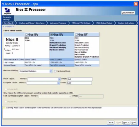
[image:4.595.330.557.77.284.2]The Nios II processor is a configurable soft IP core, as opposed to a fixed, off-the-shelf Microcontroller. It can add or remove features on a system-by-system basis to meet performance or design requirement. Soft means the processor core is not fixed in silicon and can be targeted to any Altera FPGA family. For configuration of CPU user have to choose appropriate Nios II soft core processor which comes with 3 different configuration levels. Users also have to set Exception & Reset addresses for selected CPU. So, as per performance & throughput requirement user can choose any of the CPU is as shown in Figure-2 below.
Figure-2 Configuration of Nios II CPU
5.4
SOPC builder system overview
SOPC builder allows us to design the structure of hardware system as per requirement. The GUI allows adding components to a system configure components & specify the connectivity of final system. Overview of SOPC generated System is shown in Figure-3 as follows:
Figure-3 SOPC System
[image:4.595.337.555.401.579.2]An SOPC Builder component is usually composed of the following four types of files:
1. HDL files—define the component’s functionality as hardware.
2. Hardware Component Description File (_hw.tcl) — describes the SOPC Builder related characteristics, such as interface behaviors. This file is created by the component editor.
3. C-language files—define the component register map and driver software to allow programs to control the component.
4. Software Component Description File (_sw.tcl) file—used by the software build tools to use and compile the component driver code
5.5
Final System on FPGA
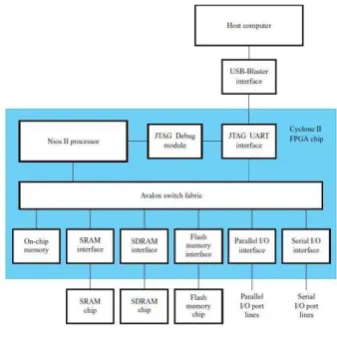
[image:5.595.318.563.72.222.2]Nios II processor and the interfaces needed to connected together which are implemented in the Cyclone II FPGA chip as in Figure-4 below
Figure-4 FPGA System
[image:5.595.83.252.303.474.2]Components are interconnected by means of the interconnection network called the Avalon Switch Fabric. The memory blocks in the Cyclone II device can be used to provide an on-chip memory for the Nios II processor. JTAG Debug module, is provided to allow the host computer to control the Nios II system. It makes it possible to perform operations such as downloading programs into memory, starting and stopping execution, setting breakpoints, and collecting real-time execution trace data .all parts of the Nios II system implemented on the FPGA chip are defined by using a hardware description language which is generated using SOPC Technology. Schematic view of System is as in Figure-5 shown below
Figure-5 Schematic View
6.
COMPARISON OF SOFT CORE
PROCESSOR
To compare the performance of Implemented Soft processor, we consider the works that are available for FPGA. It may be noted from Table-1 all Soft Processor which are implemented on FPGA are Optimized & Configured [10] according to application requirements.
Table-1 Embedded Soft Core Processor for FPGA
Soft Core Processor
Architecture Area(LE) Supported FPGA
LEON3 SPARC-v8 3500 Xlinx FPGA
Microblaze Microblaze 1324 Xlinx FPGA Picoblaze Picoblaze 192 Xlinx FPGA Cortex-M1 ARMv6 2600 Xlinx &
Altera FPGA Nios II NIos II Nios II(f)-1800 Altera FPGA
Nios II(s)-1700 Nios II(e)-390
From above table if we compare Nios II soft processor with other soft Core processor it increases configuration level by allowing to select either fast, slow or economy processor for application & which gives performance in terms of area optimization. Each Implemented Soft processor supports their respective Architecture which is different for all application & FPGA also.
7.
CONCLUSION
[image:5.595.311.555.354.474.2]8.
REFERENCES
[1] Zuo Zhen, Tang Guilin , Dong Zhi , Huang Zhiping ,”Design and realization of the hardware platform based on the Nios soft-core processor” 8th International Conference on Electronic Measurement and Instruments, ICEMI '07, Proc. IEEE,pg.865-869,July2007
[2] Alcalde, Ortmann, M.S, Mussa, S.A. ,“NIOS II Processor Implemented in FPGA: An Application on Control of a PFC Converter” Conference on Power Electronics Specialists , PESC 2008.Proc. IEEE , pg.4446-4451,June 2008.
[3] Wang Ziting ,Guo Haili ,Sun Yan ,“Design of VGA Image Controller Based on SOPC Technology”
International Conference onNew Trends in Information and Service Science, NISS '09, Proc. IEEE,pg.825-827 , July 2009.
[4] Lin Fei-yu , Jiao Xi-xiang , Guo Yu-Hui , Zhang Jian-chuan , Qiao Wei-ming , Jing Lan , Wang Yan-Yu , Ma Yan-Yun-hai ,“System On Programmable Chip Development System” Second International Workshop on Education Technology and Computer Science (ETCS), proc. IEEE , Volume 1,pg.471-474, March2010.
[5] Cardarilli, G.C. Di Nunzio, L., Fazzolari, R. , Re, M. , Lee, R.B. ,“Butterfly and Inverse Butterfly nets integration on Altera NIOS-II embedded processor” Forty Fourth Asilomar Conference on Signals, Systems and Computers (ASILOMAR), 2010 , Proc. IEEE,pg.1279-1283,Nov 2010.
[6] Tong, J.G. ,Anderson, I.D.L. ,Khalid, M.A.S. ,“ Soft- Core Processors for Embedded Systems ” Sixth International Conference on Microelectronics, proc. IEEE, pg.170-173, Dec2006.
[7] First time designer guide
http://www.altera.com/literature/hb/nios2/edh_ed51001.p df
[8] SOPC guide
http://www.altera.com/literature/ug/ug_sopc_builder.pdf [9] Quartus II Version 7.2 Handbook Volume 4: SOPC
Builder:
http://www.cs.columbia.edu/~sedwards/classes/2008/484 0/qts_qii5v4.pdf