3A Fast-Response LDO Regulator
Super ßeta PNP is a registered trademark of Micrel, Inc.
Micrel Inc. • 2180 Fortune Drive • San Jose, CA 95131 • USA • tel +1 (408) 944-0800 • fax + 1 (408) 474-1000 • http://www.micrel.com
October 3, 2014 Revision 2.0
General Description
The MIC29302A is a high-current, low-cost, low-dropout voltage regulator that uses Micrel's proprietary Super βeta PNP® process with a PNP pass element. The 3A LDO regulator features 450mV (full load) dropout voltage and very low ground current. Designed for high-current loads, these devices also find applications in lower current, low-dropout critical systems, where their low-dropout voltages and ground current values are important attributes.
Along with a total accuracy of ±2% (over temperature, line, and load regulation) the regulator features very fast transient recovery from input voltage surges and output load current changes.
The MIC29302A has an adjustable output that can be set by two external resistors to a voltage between 1.24V and 15V. In addition, the device is fully protected against overcurrent faults, reversed input polarity, reversed lead insertion, and overtemperature operation. A TTL logic enable (EN) pin is available in the MIC29302A to shutdown the regulator. When not used, the device can be set to continuous operation by connecting EN to the input (IN). The MIC29302A is available in the standard and 5-pin TO-263 and TO-252 packages with an operating junction temperature range of −40°C to +125°C.
Datasheets and support documentation can be found on Micrel’s website at: www.micrel.com.
Features
• High-current capability
− 3A over full temperature range
• Low-dropout voltage of 450mV at full load
• Low ground current
• Accurate 1% guaranteed tolerance
• Extremely fast transient response
• Zero-current shutdown mode
• Error flag signals output out-of-regulation
• Adjustable output voltage
• Packages: TO-263-5L and TO-252-5L
Applications
• Processor peripheral and I/O supplies
• High-efficiency “green” computer systems
• Automotive electronics
• High-efficiency linear lower supplies
• Battery-powered equipment
• PC add-in cards
• High-efficiency post-regulator for switching supply
_________________________________________________________________________________________________________________________
Typical Application
+ × = 1 R2 R1 1.242 VOUT Dropout Voltage vs. Output Current0 100 200 300 400 500
0.0 0.5 1.0 1.5 2.0 2.5 3.0 OUTPUT CURRENT (A)
D R OP OU T V OL T A GE ( m V )
VIN = 3.3V VADJ = 0V
October 3, 2014 2 Revision 2.0
Ordering Information
Part Number Voltage Junction Temperature Range Package
MIC29302AWU Adjustable –40°C to +125°C 5-Pin TO-263
MIC29302AWD Adjustable –40°C to +125°C 5-Pin TO-252
Pin Configuration
5-Pin TO-263 (D2Pak) Adjustable Voltage (U) MIC29302AWU
5-Pin TO-252 (D-Pak) Adjustable Voltage (D) MIC29302AWD
Pin Description
Pin Number TO-263
Pin Number
TO-252 Pin Name Pin Function
1 1 EN Enable (Input): Active-high CMOS compatible control input. Do not float.
2 2 IN INPUT: Unregulated input, +3V to +16V maximum
3, TAB 3, TAB GND GND: TAB is also connected internally to the IC’s ground on both packages.
4 4 OUT OUTPUT: The regulator output voltage
October 3, 2014 3 Revision 2.0
Absolute Maximum Ratings
(1)Input Supply Voltage (VIN)(1) ... –20V to +20V
Enable Input Voltage (VEN) ... –0.3V to VIN
Lead Temperature (soldering, 5 sec.) ... 260°C Power Dissipation ... Internally Limited Storage Temperature Range ... –65°C to +150°C ESD Rating all pins(3)
Operating Ratings
(2)Operating Junction Temperature ... −40°C to +125°C Operating Input Voltage ... 3V to 16V Package Thermal Resistance
TO-263 (θJC) ... 3°C/W
TO-252 (θJC) ... 3°C/W
TO-252 (θJA) ... 35°C/W
TO-263 (θJA) ... 28°C/W
Electrical Characteristics
(4)VIN = 4.2V; IOUT = 100mA; TA = 25°C, bold values indicate −40°C≤ TJ≤ +125°C, unless noted.
Parameter Condition Min. Typ. Max. Units
Output Voltage
Output Voltage Accuracy(5) 100mA ≤ IOUT≤3A, (VOUT+ 1V) ≤ VIN≤ 16V −2 2 %
Line Regulation IOUT = 100mA, (VOUT + 1V) ≤ VIN≤ 16V 0.1 0.5 %
Load Regulation VIN = VOUT + 1V, 100mA ≤ IOUT≤ 3A 0.2 1 %
Dropout Voltage(6)
IOUT = 100mA 80 200
mV
IOUT = 750mA 220
IOUT = 1.5A 275
IOUT = 2.0A 375 630
IOUT = 2.5A 430 720
IOUT = 3A 450 800
Ground Current
Ground Current
IOUT = 750mA, VIN = VOUT + 1V 5 20
mA
IOUT = 1.5A 15
IOUT = 3A 60 150
IGRNDDO Ground Pin Current
@ Dropout VIN = 0.5V less than specified VOUT× IOUT = 10mA 2
Current Limit VOUT = 0V(7) 3 4 A
en, Output Noise Voltage
(10Hz to 100kHz CL = 10µF 400 µVRMS
IL = 100mA CL = 33µF 260
Ground Pin Current in Shutdown Input Voltage VIN = 16V 32 µA
Notes:
1. Exceeding the absolute maximum rating may damage the device. 2. The device is not guaranteed to function outside its operating rating.
3. Devices are ESD sensitive. Handling precautions recommended. Human body model, 1.5kΩ in series with 100pF. 4. Specification for packaged product only
5. Output voltage temperature coefficient is defined as the worst case voltage change divided by the total temperature change.
6. Dropout voltage is defined as the input-to-output differential when output voltage drops to 99% of its normal value with VOUT + 1V applied to VIN. 7. VIN =VOUT (nominal) + 1V. For example, use VIN = 4.3V for a 3.3V regulator or use 6V for a 5V regulator. Employ pulse testing procedure for current limit.
October 3, 2014 4 Revision 2.0
Electrical Characteristics
(4)(Continued)
VIN = 4.2V; IOUT = 10mA; TA = 25°C, bold values indicate −40°C≤ TJ≤ +125°C, unless noted. Reference
Reference Voltage Note 8 1.215 1.267 V
Adjust Pin Bias Current 40 nA
120 ENABLE Input
Input Logic Voltage Low (OFF) 0.8 V
High (ON) 2.4
Enable Pin Input Current
VEN = 4.2V
15 30
µA
75
VEN = 0.8V
2
4
Regulator Output Current
in Shutdown Note 10
10
µA
20
Notes:
8. VREF≤ VOUT≤ VIN -1, 3V ≤ VOUT≤ 16V, 10mA ≤ IL≤ IFL, TJ≤TJmax.
9. Thermal regulation is defined as the change in the output voltage at a time T after a change in power dissipation is applied, excluding load or line regulation effects. Specifications are for a 250mA load pulse at VIN = 16V (a 4W pulse) for T = 10ms.
October 3, 2014 5 Revision 2.0
Typical Characteristics
Dropout Voltage vs. Input Voltage
0 100 200 300 400 500
0 4 8 12 16
INPUT VOLTAGE (V)
D R OP OU T V OL T A GE ( m V )
IOUT = 3A
IOUT = 1.0A
GND Pin Current vs. Input Voltage
0.0 10.0 20.0 30.0 40.0 50.0 60.0 70.0
0 4 8 12 16
INPUT VOLTAGE (V)
G RO UND CURRE NT ( m
A) IOUT = 3A
Adjust Pin Voltage vs. Input Voltage
1.230 1.235 1.240 1.245 1.250
0 4 8 12 16
INPUT VOLTAGE (V)
A D J P IN V O L T A G E ( V
) VOUT = 1.8V
IOUT = 3A
Adjust Pin Current vs. Input Voltage
40 42 44 46
0 4 8 12 16
INPUT VOLTAGE (V)
ADJ P IN CURRE NT ( n A)
ILOAD = 10mA
Load Regulation vs. Input Voltage
0.000 0.100 0.200 0.300
0 4 8 12 16
INPUT VOLTAGE (V)
L O AD RE G UL AT IO N ( %
) VOUT = 1.8V
IOUT = 10mA to 3A
Short-Circuit Current vs. Input Voltage
0 2 4 6 8 10
0 4 8 12 16
INPUT VOLTAGE (V)
CURRE NT L IM IT ( A)
VOUT = 0V
Enable Pin Current vs. Input Voltage
0.00 5.00 10.00 15.00 20.00
0 4 8 12 16
INPUT VOLTAGE (V)
E NABL E P IN CURRE NT ( µ A)
VOUT = 1.8V
IOUT = 10mA
VEN = VIN
Output Voltage vs. Input Voltage
1.240 1.241 1.242 1.243
0 4 8 12 16
INPUT VOLTAGE (V)
O U TP U T V O LTA G E ( V )
VOUT = 1.24V
IOUT = 10mA
October 3, 2014 6 Revision 2.0
Typical Characteristics (Continued)
GND Pin Current vs. Temperature 0.00 2.00 4.00 6.00 8.00 10.00
-50 -25 0 25 50 75 100 125
TEMPERATURE (°C) G RO UND CURRE NT ( m A)
VIN =4.2V
VOUT = 1.8V
IOUT = 750mA
0 5 10 15 20 25 30
-50 -25 0 25 50 75 100 125
E N P IN CURRE NT ( n A ) TEMPERATURE (°C)
Enable Bias Current vs. Temperature
VIN= VEN= 8V
VOUT= 2.5V
IOUT= 10mA
Dropout Voltage vs. Temperature 0 100 200 300 400 500 600
-50 -25 0 25 50 75 100 125
TEMPERATURE (°C) D R OP OU T V OL T A GE ( m V )
VIN = 4.2V
IOUT = 1.5A
IOUT = 3A
Dropout Voltage vs. Temperature 0 100 200 300 400
-50 -25 0 25 50 75 100 125
TEMPERATURE (°C) D R OP OU T V OL T A GE ( m V ) V
IN = 4.2V
IOUT = 750mA
IOUT = 100mA
Short-Circuit Current vs. Temperature 3.500 3.750 4.000 4.250
-50 -25 0 25 50 75 100 125
TEMPERATURE (°C) CURRE NT L IM IT ( A)
VIN = 4.2V
VOUT = 0V
Adjust Pin Voltage vs. Temperature
1.235 1.238 1.240 1.243
-50 -25 0 25 50 75 100 125
TEMPERATURE (°C) A D J P IN V O L T A G E ( V )
VIN =4.2V
VOUT = 1.8V
IOUT = 10mA
Adjust Pin Current vs. Temperature 0 20 40 60 80
-50 -25 0 25 50 75 100 125
TEMPERATURE (°C) ADJ P IN CURRE NT ( n A)
VIN = 4.2V
ILOAD = 10mA
Line Regulation vs. Temperature 0.0 0.1 0.2 0.3 0.4 0.5
-50 -25 0 25 50 75 100 125
TEMPERATURE (°C) L IN E R E GU L A T ION ( % /V
) VVIN = 3V to 16V
OUT = 1.8V
October 3, 2014 7 Revision 2.0
Typical Characteristics (Continued)
Dropout Voltage vs. Output Current
0 100 200 300 400 500
0.0 0.5 1.0 1.5 2.0 2.5 3.0
OUTPUT CURRENT (A)
D R OP OU T V OL T A GE ( m V
) VIN = 3V
VADJ = 0V
ADJUSTABLE OPTION
Dropout Voltage vs. Output Current
0 100 200 300 400 500
0.0 0.5 1.0 1.5 2.0 2.5 3.0
OUTPUT CURRENT (A)
D R OP OU T V OL T A GE ( m V
) VIN = 4.2V
VADJ = 0V
Adjust Pin Voltage vs. Output Current
1.236 1.238 1.240 1.242 1.244 1.246
0.0 0.5 1.0 1.5 2.0 2.5 3.0
OUTPUT CURRENT (A)
A D J P IN V O L T A G E ( V
) VIN = 4.2V
VOUT = 1.8V
Line Regulation vs. Output Current
-0.2 -0.1 0.0 0.1 0.2
0.0 0.5 1.0 1.5 2.0 2.5 3.0
OUTPUT CURRENT (A)
L INE RE G UL AT IO N ( % )
VIN = 4.2V to 16V
VOUT = 1.8V
GND Pin Current vs. Output Current
0 10 20 30 40 50 60 70
0.0 0.5 1.0 1.5 2.0 2.5 3.0
OUTPUT CURRENT (A)
G RO UND CURRE NT ( m
A) VVIN = 4.2V
OUT = 1.8V
Output Noise vs. Frequency 0.001 0.01 0.1 1 10 100 1000
0.01 0.1 1 10 100 1000
FREQUENCY (kHz) OU TP U T N OIS E ( µV /√ H
z) Noise SpectralDensity
VIN =3.3V
VOUT = 1.8V
IOUT = 3A
COUT = 47µF
Ripple Rejection (IOUT = 10mA)
vs. Frequency 0 10 20 30 40 50 60 70 80
0.01 0.1 1 10 100 1000
FREQUENCY (kHz) R IP P L E R E J E C T IO N ( d B ) Gain (dB)
VIN =3.3V
VOUT = 1.8V
IOUT = 10mA
COUT = 22µF
Ripple Rejection (IOUT = 1.5A)
vs. Frequency 0 10 20 30 40 50 60 70 80
0.01 0.1 1 10 100 1000
FREQUENCY (kHz) R IP P L E R E J E C T IO N ( d B ) Gain (dB)
VIN =3.3V
VOUT = 1.8V
IOUT = 1.5A
COUT = 22µF
Ripple Rejection (IOUT = 3A)
vs. Frequency 0 10 20 30 40 50 60 70 80
0.01 0.1 1 10 100 1000
FREQUENCY (kHz) R IP P L E R E J E C T IO N ( d B ) Gain (dB)
VIN =3.3V
VOUT = 1.8V
IOUT = 3A
October 3, 2014 8 Revision 2.0
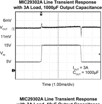
Functional Characteristics
October 3, 2014 9 Revision 2.0
October 3, 2014 10 Revision 2.0
Application Information
The MIC29302A is a high-performance, low-dropout voltage regulator suitable for all moderate to high-current voltage regulation applications. Its 450mV typical dropout voltage at full load makes it especially valuable in battery-powered systems and as high efficiency noise filters in post-regulator applications. Unlike older NPN-pass transistor designs, where the minimum dropout voltage is limited by the base-emitter voltage drop and collector-emitter saturation voltage, dropout performance of the PNP output is limited merely by the low VCE
saturation voltage.
A trade-off for the low-dropout voltage is a varying base driver requirement. But Micrel’s Super ßeta PNP® process reduces this drive requirement to merely 1% of the load current.
The MIC29302A regulator is fully protected from damage due to fault conditions. Current limiting is linear; output current under overload conditions is constant. Thermal shutdown disables the device when the die temperature exceeds the +125°C maximum safe operating temperature. The output structure of the regulators allows voltages in excess of the desired output voltage to be applied without reverse current flow. The MIC29302A offers a logic-level ON/OFF control. When disabled, the device draws nearly zero current.
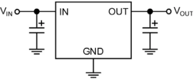
Figure 2. Linear Regulators Require Only Two Capacitors for Operation
Thermal Design
Linear regulators are simple to use. The most complicated set of design parameters to consider are thermal characteristics. Thermal design requires the following application-specific parameters:
• Maximum ambient temperature, TA
• Output Current, IOUT
• Output Voltage, VOUT
• Input Voltage, VIN
First, we calculate the power dissipation of the regulator from these numbers and the device parameters from this datasheet:
(
IN OUT)
OUT
D I 1.02V V
P = −
Where the ground current is approximated by 2% of IOUT.
Then the heatsink thermal resistance is determined with this formula:
(
JC CS)
DA JMAX
SA θ θ
P T T
θ = − − +
where:
TJMAX≤ 125°C and θCS is between 0°C/W and 2°C/W.
The heatsink may be significantly reduced in applications where the minimum input voltage is known and is large compared to the dropout voltage. A series input resistor can be used to drop excessive voltage and distribute the heat between this resistor and the regulator. The low-dropout properties of Micrel Super βeta PNP®
regulators allow very significant reductions in regulator power dissipation and the associated heatsink without compromising performance. When this technique is employed, a capacitor of at least 0.1µF is needed directly between the input and regulator ground.
Please refer to Application Note 9 and Application Hint 17 on Micrel’s website (www.micrel.com) for further details and examples on thermal design and heatsink specification.
With no heatsink in the application, calculate the junction temperature to determine the maximum power dissipation that will be allowed before exceeding the maximum junction temperature of the MIC29302A. The maximum power allowed can be calculated using the thermal resistance (θJA) of the D-Pak (TO252) adhering
to the following criteria for the PCB design: 2oz. copper and 100mm2 copper area for the MIC29302A.
For example, given an expected maximum ambient temperature (TA) of 75°C with VIN = 3.3V, VOUT = 2.5V,
and IOUT = 3A, first calculate the expected PD using:
(
3.3V 2.5V)
3A(
3.3V) (
0.016A)
2.3472WPD= − × − × =
October 3, 2014 11 Revision 2.0
Next, calcualte the junction temperature for the expected power dissipation:
TJ = (θJA×PD) + TA = (35°C/W × 2.3472W)
+ 75°C = 157.15°C
Now determine the maximum power dissipation allowed that would not exceed the IC’s maximum junction temperature (125°C) without the use of a heatsink by:
PD(MAX) = (TJ(MAX) – TA) / θJA
= (125°C – 75°C) / (35°C/W) = 1.428W
Capacitor Requirements
For stability and minimum output noise, a capacitor on the regulator output is necessary. The value of this capacitor is dependent upon the output current; lower currents allow smaller capacitors. The MIC29302A is stable with a 10μF capacitor at full load.
This capacitor need not be an expensive low-ESR type; aluminum electrolytics are adequate. In fact, extremely low-ESR capacitors may contribute to instability. Tantalum capacitors are recommended for systems where fast load transient response is important.
When the regulator is powered from a source with high AC impedance, a 0.1µF capacitor connected between input and GND is recommended.
Transient Response and 5V to 3.3V Conversion
The MIC29302A has excellent response to variations in input voltage and load current. By virtue of its low dropout voltage, the device does not saturate into dropout as readily as similar NPN-based designs. A 3.3V output Micrel LDO will maintain full speed and performance with an input supply as low as 4.2V, and will still provide some regulation with supplies down to 3.8V, unlike NPN devices that require 5.1V or more for good performance and become nothing more than a resistor under 4.6V of input. Micrel’s PNP regulators provide superior performance in “5V to 3.3V” conversion applications than NPN regulators, especially when all tolerances are considered.
Minimum Load Current
The MIC29302A regulator operates within a specified load range. If the output current is too small, leakage currents dominate and the output voltage rises.
A minimum load current of 10mA is necessary for proper regulation and to swamp any expected leakage current across the operating temperature range.
For best performance the total resistance (R1+R2) should be small enough to pass the minimum regulator load current of 10mA.
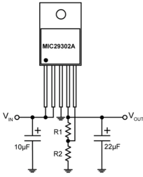
Adjustable Regulator Design
The output voltage can be programmed anywhere between 1.25V and the 15V. Two resistors are used. The resistor values are calculated by:
− ×
= 1
1.240 V R
R1 2 OUT
where VOUT is the desired output voltage.
Figure 3 shows component definition. Applications with widely varying load currents may scale the resistors to draw the minimum load current required for proper operation (see “Minimum Load Current” section).
Figure 3. Adjustable Regulator with Resistors
Enable Input
MIC29302A features an enable (EN) input that allows ON/OFF control of the device. Special design allows “zero” current drain when the device is disabled—only microamperes of leakage current flows. The EN input has TTL/CMOS compatible thresholds for simple interfacing with logic, or may be directly tied to VIN.
Enabling the regulator requires approximately 20µA of current into the EN pin.
October 3, 2014 12 Revision 2.0
October 3, 2014 13 Revision 2.0
Bill of Materials
Item Part Number Manufacturer Description Qty.
C1 C2012X5R1E106K TDK(11) 10µF, 25V, Ceramic Capacitor, X5R, 0805 1
C2,C3 B45196H4106K309 Kemet
(12)
10µF, 20V, Tantalum Capacitor, 2312 2
TR3C106K020C0450 Vishay(13)
C5 EEU-FM1E102 Panasonic(14) 1000µF, 25V, Elect Capacitor, through hole, 10X22-case 1
C6 T495D107K016ATE125 Kemet 100µF, 20V, Tantalum Capacitor, 2917 1
TR3D107K016C0125 Vishay
R1 CRCW06031K00FKTA Vishay 1k, Resistor, 1%, 0603 1
R2 Open (CRCW06031002FRT1) Vishay 10k, Resistor, 1%, 0603 1
R3 CRCW06038061FRT1 Vishay 8.06k, Resistor, 1%, 0603 1
R4 CRCW06034751FRT1 Vishay 4.75k, Resistor, 1%, 0603 1
R5 CRCW06033241FRT1 Vishay 3.24k, Resistor, 1%, 0603 1
R6 CRCW06031911RFRT1 Vishay 1.91k, Resistor, 1%, 0603 1
R7 CRCW06030000FKTA Vishay 0Ω, Resistor, 1%, 0603 1
R8 CRCW060350R0FRT1 Vishay 50Ω, Resistor, 1%, 0603 1
U1 MIC29302AWU Micrel(15) 3A Fast-Response LDO Regulator 1
Notes:
11. TDK: www.tdk.com. 12. Kemet: www.kemet.com. 13. Vishay: www.vishay.com. 14. Panasonic.: www.panasonic.com. 15. Micrel, Inc.: www.micrel.com.
October 3, 2014 14 Revision 2.0
PCB Layout Recommendations
MIC29302A Evaluation Board Top Layer
October 3, 2014 15 Revision 2.0
PCB Layout Recommendations (Continued)
MIC29302A Evaluation Board Bottom Layer
October 3, 2014 16 Revision 2.0
Package Information
(16)5-Pin TO-263 (U)
Note:
October 3, 2014 17 Revision 2.0
Package Information (Continued)
October 3, 2014 18 Revision 2.0
MICREL, INC. 2180 FORTUNE DRIVE SAN JOSE, CA 95131 USA
TEL +1 (408) 944-0800 FAX +1 (408) 474-1000 WEB http://www.micrel.com
Micrel, Inc. is a leading global manufacturer of IC solutions for the worldwide high performance linear and power, LAN, and timing & communications markets. The Company’s products include advanced mixed-signal, analog & power semiconductors; high-performance communication, clock management, MEMs-based clock oscillators & crystal-less clock generators, Ethernet switches, and physical layer transceiver ICs. Company customers include leading manufacturers of enterprise, consumer, industrial, mobile, telecommunications, automotive, and computer products. Corporation headquarters and state-of-the-art wafer fabrication facilities are located in San Jose, CA, with regional sales and support offices and advanced technology design centers situated throughout the Americas, Europe, and Asia. Additionally, the Company maintains an extensive network of distributors and reps worldwide.
Micrel makes no representations or warranties with respect to the accuracy or completeness of the information furnished in this datasheet. This information is not intended as a warranty and Micrel does not assume responsibility for its use. Micrel reserves the right to change circuitry, specifications and descriptions at any time without notice. No license, whether express, implied, arising by estoppel or otherwise, to any intellectual property rights is granted by this document. Except as provided in Micrel’s terms and conditions of sale for such products, Micrel assumes no liability whatsoever, and Micrel disclaims any express or implied warranty relating to the sale and/or use of Micrel products including liability or warranties relating to fitness for a particular purpose, merchantability, or infringement of any patent, copyright, or other intellectual property right.
Micrel Products are not designed or authorized for use as components in life support appliances, devices or systems where malfunction of a product can reasonably be expected to result in personal injury. Life support devices or systems are devices or systems that (a) are intended for surgical implant into the body or (b) support or sustain life, and whose failure to perform can be reasonably expected to result in a significant injury to the user. A Purchaser’s use or sale of Micrel Products for use in life support appliances, devices or systems is a Purchaser’s own risk and Purchaser agrees to fully indemnify Micrel for any damages resulting from such use or sale.