CHAPTER 1: THE OP AMP
INTRODUCTION 1.1
SECTION 1.1: OP AMP OPERATION
1.3INTRODUCTION 1.3
VOLTAGE FEEDBACK (VFB) MODEL 1.3
BASIC OPERATION 1.4
INVERTING AND NONINVERTING CONFIGURATIONS 1.5
OPEN-LOOP GAIN 1.9
GAIN BANDWIDTH PRODUCT 1.11
STABILITY CRITERIA 1.11 PHASE MARGIN 1.13 CLOSED-LOOP GAIN 1.13 SIGNAL GAIN 1.14 NOISE GAIN 1.14 LOOP GAIN 1.15 BODE PLOT 1.16
CURRENT FEEDBACK (CFB) MODEL 1.17
DIFFERENCES FROM VFB 1.17
HOW TO CHOOSE BETWEEN VFB AND CFB 1.19
SUPPLY VOLTAGES 1.19
SINGLE-SUPPLY CONSIDERATIONS 1.20
CIRCUIT DESIGN CONSIDERATIONS FOR SINGLE-
SUPPLY SYSTEMS 1.23
RAIL-TO-RAIL 1.25
PHASE REVERSAL 1.25
LOW POWER AND MICROPOWER 1.25
PROCESSES 1.26
EFFECTS OF OVERDRIVE ON OP AMP INPUTS 1.27
SECTION 1.2: OP AMP SPECIFICATIONS
1.29INTRODUCTION 1.29
DC SPECIFICATIONS 1.30
OPEN-LOOP GAIN 1.30
OPEN-LOOP TRANSRESISTANCE OF A CFB OP AMP 1.32
OFFSET VOLTAGE 1.33
OFFSET VOLTAGE DRIFT 1.33
DRIFT WITH TIME 1.33
SECTION 1.2: OP AMP SPECIFICATIONS (cont.)
CORRECTION FOR OFFSET VOLTAGE 1.34
DigiTrim™ TECHNOLOGY 1.34
EXTERNAL TRIM 1.36
INPUT BIAS CURRENT 1.38
INPUT OFFSET CURRENT 1.38
COMPENSATING FOR BIAS CURRENT 1.39
CALCULATING TOTAL OUTPUT OFFSET ERROR DUE TO
INPUT IMPEDANCE 1.42
INPUT CAPACITANCE 1.43
INPUT COMMON MODE VOLTAGE RANGE 1.43
DIFFERENTIAL INPUT VOLTAGE 1.44
SUPPLY VOLTAGES 1.44
QUIESCENT CURRENT 1.44
OUTPUT VOLTAGE SWING
(OUTPUT VOLTAGE HIGH / OUTPUT VOLTAGE LOW) 1.45
OUTPUT CURRENT (SHORT-CIRCUIT CURRENT) 1.45
AC SPECIFICATIONS 1.47 NOISE 1.47 VOLTAGE NOISE 1.47 NOISE BANDWIDTH 1.48 NOISE FIGURE 1.48 CURRENT NOISE 1.49
TOTAL NOISE (SUM OF NOISE SOURCES) 1.49
1/f NOISE (FLICKER NOISE) 1.51
POPCORN NOISE 1.52
RMS NOISE CONSIDERATIONS 1.53
TOTAL OUTPUT NOISE CALCULATIONS 1.55
DISTORTION 1.60
THD (TOTAL HARMONIC DISTORTION) 1.60
THD + N (TOTAL HARMONIC DISTORTION PLUS NOISE) 1.60
INTERMODULATION DISTORTION 1.61
THIRD+C65 ORDER INTERCEPT POINT (IP3), SECOND
ORDER C56 INTERCEPT POINT (IP2) 1.61
1 dB COMPRESSION POINT 1.63
SNR (SIGNAL TO NOISE RATIO) 1.63
ENOB (EQUIVALENT NUMBER OF BITS) 1.63
OP AMP SPECIFICATIONS (cont.)
SPURIOUS-FREE DYNAMIC RANGE (SFDR) 1.64
SLEW RATE 1.64
FULL POWER BANDWIDTH 1.65
−3 dB SMALL SIGNAL BANDWIDTH 1.66
BANDWIDTH FOR 0.1 dB BANDWIDTH FLATNESS+C65 1.66
GAIN-BANDWIDTH PRODUCT 1.67
CFB FREQUENCY DEPENDANCE 1.68
SETTLING TIME 1.69
RISE TIME AND FALL TIME 1.70
PHASE MARGIN 1.70
CMRR (COMMON-MODE REJECTION RATIO) 1.71
PSRR (POWER SUPPLY REJECTION RATIO) 1.72
DIFFERENTIAL GAIN 1.73
DIFFERENTIAL PHASE 1.75
PHASE REVERSAL 1.75
CHANNEL SEPARATION 1.75
SECTION 1.3: HOW TO READ DATA SHEETS
1.83THE FRONT PAGE 1.83
THE SPECIFICATION TABLES 1.83
THE ABSOLUTE MAXIMUMS 1.89
THE ORDERING GUIDE 1.92
THE GRAPHS 1.92
THE MAIN BODY 1.93
SECTION 1.4: CHOOSING AN OP AMP
1.95STEP 1: DETERMINE THE PARAMETERS 1.96
CHAPTER 1: THE OP AMP
Introduction
In this chapter we will discuss the basic operation of the op amp, one of the most common linear design building blocks.
In section 1 the basic operation of the op amp will be discussed. We will concentrate on the op amp from the black box point of view. There are a good many texts that describe the internal workings of an op amp, so in this work a more macro view will be taken. There are a couple of times, however, that we will talk about the insides of the op amp. It is unavoidable.
In section 2 the basic specifications will be discussed. Some techniques to compensate for some of the op amps limitations will also be given.
Section 3 will discuss how to read a data sheet. The various sections of the data sheet and how to interpret what is written will be discussed.
SECTION 1: OP AMP OPERATION
Introduction
The op amp is one of the basic building blocks of linear design. In its classic form it consists of two input terminals, one of which inverts the phase of the signal, the other preserves the phase, and an output terminal. The standard symbol for the op amp is given in Figure 1.1. This ignores the power supply terminals, which are obviously required for operation.
Figure 1.1: Standard op amp symbol
The name “op amp” is the standard abbreviation for operational amplifier. This name comes from the early days of amplifier design, when the op amp was used in analog computers. (Yes, the first computers were analog in nature, rather than digital). When the basic amplifier was used with a few external components, various mathematical “operations” could be performed. One of the primary uses of analog computers was during WWII, when they were used for plotting ordinance trajectories.
Voltage Feedback (VFB) Model
The classic model of the voltage feedback op amp incorporates the following characteristics:
1.) Infinite input impedance 2) Infinite bandwidth 3) Infinite gain
4) Zero output impedance 5) Zero power consumption
INPUTS (+) (-) INPUTS (+) (-)
None of these can be actually realized, of course. How close we come to these ideals determines the quality of the op amp.
This is referred to as the voltage feedback model. This type of op amp comprises nearly all op amps below 10 MHz bandwidth and on the order of 90% of those with higher bandwidths.
Figure 1.2: The Attributes of an Ideal Op Amp
Basic Operation
The basic operation of the op amp can be easily summarized. First we assume that there is a portion of the output that is fed back to the inverting terminal to establish the fixed
IDEAL OP AMP ATTRIBUTES
Infinite Differential Gain Zero Common Mode Gain Zero Offset Voltage Zero Bias Current Infinite Bandwidth
OP AMP INPUT ATTRIBUTES
Infinite Impedance Zero Bias Current
Respond to Differential Voltages
Do Not Respond to Common Mode Voltages
OP AMP OUTPUT ATTRIBITES
Zero Impedance OP AMP OUTPUT POSITIVE SUPPLY NEGATIVE SUPPLY INPUTS (+) (-) OP AMP OUTPUT POSITIVE SUPPLY NEGATIVE SUPPLY INPUTS (+) (-)
terminals of the op amp is multiplied by the amplifier’s open-loop gain. If the magnitude of this differential voltage is more positive on the inverting (-) terminal than on the noninverting (+) terminal, the output will go more negative. If the magnitude of the differential voltage is more positive on the noninverting (+) terminal than on the inverting (-) terminal, the output voltage will become more positive. The open-loop gain of the amplifier will attempt to force the differential voltage to zero. As long as the input and output stays in the operational range of the amplifier, it will keep the differential voltage at zero, and the output will be the input voltage multiplied by the gain set by the feedback. Note from this that the inputs respond to differential mode not common-mode input voltage.
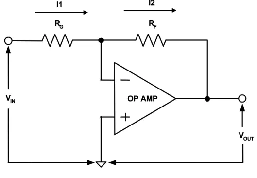
Inverting and Noninverting Configurations
There are two basic ways to configure the voltage feedback op amp as an amplifier. These are shown in Figure 1.3 and Figure 1.4.
Figure 1.3 shows what is known as the inverting configuration. With this circuit, the output is out of phase with the input. The gain of this circuit is determined by the ratio of the resistors used and is given by:
Figure 1.3: Inverting Mode Op Amp Stage
Eq. 1-1 VIN = - RF/RG VOUT OP AMP RF RG G = VOUT/VIN SUMMING POINT A = - Rfb R in Rfb R in Rfb R in Rfb R in A = - Rfb R in Rfb R in Rfb R in Rfb R in A = - Rfb R in Rfb R in Rfb R in Rfb R in
Figure 1.4 shows what is know as the noninverting configuration. With this circuit the output is in phase with the input. The gain of the circuit is also determined by the ratio of the resistors used and is given by:
Figure 1.4: Noninverting Mode Op Amp Stage
Note that since the output drives a voltage divider (the gain setting network) the maximum voltage available at the inverting terminal is the full output voltage, which yields a minimum gain of 1.
Also note that in both cases the feedback is from the output to the inverting terminal. This is negative feedback and has many advantages for the designer. These will be discussed more in detail further in this chapter.
It should also be noted that the gain is based on the ratio of the resistors, not their actual values. This means that the designer can choose just about any value he wishes within practical limits.
If the values of the resistors are too low, a great deal of current would be required from the op amps output for operation. This causes excessive dissipation in the op amp itself, which has many disadvantages. The increased dissipation leads to self-heating of the chip, which could cause a change in the dc characteristics of the op amp itself. Also the heat generated by the dissipation could eventually cause the junction temperature to rise above the 150°C, the commonly accepted maximum limit for most semiconductors. The junction temperature is the temperature at the silicon chip itself. On the other end of the Eq. 1-2 VIN VOUT OP AMP RF RG G = VOUT/VIN = 1 + (RF/RG) A = 1+ R fb Rinin A = 1+ R fb Rinin
susceptibility to parasitic capacitances, which could also limit bandwidth and possibly cause instability and oscillation.
From a practical sense, resistors below 10 Ω and above 1 MΩ become increasingly difficult to purchase especially if precision resistors are required.
Figure 1.5: Inverting Amplifier Gain
Let us look at the case of an inverting amp in a little more detail. Referring to Figure 1.5, the noninverting terminal is connected to ground. (We are assuming a bipolar (+ and −) power supply). Since the op amp will force the differential voltage across the inputs to zero, the inverting input will also appear to be at ground. In fact, this node is often referred to as a “virtual ground.”
If there is a voltage (Vin) applied to the input resistor, it will set up a current (I1) through the resistor (Rin) so that
Since the input impedance of the op amp is infinite, no current will flow into the inverting input. Therefore, this same current (I1) must flow through the feedback resistor (Rfb). Since the amplifier will force the inverting terminal to ground, the output will assume a voltage (Vout) such that:
I1= V R in in I1= V R in in I1= V R in in I1= V R in in V = I1 * Rout fb V = I1 * Rout fb Eq. 1.3 Eq. 1-4 VIN VOUT OP AMP RF RG I1 I2 VIN VOUT OP AMP RF RG I1 I2
Doing a little simple arithmetic we then can come to the conclusion of eq. 1.1:
Figure 1.6: Noninverting Amplifier gain
Now we examine the noninverting case in more detail. Referring to Figure 1.6, the input voltage is applied to the noninverting terminal. The output voltage drives a voltage divider consisting of Rfb and Rin. The name “Rin,” in this instance, is somewhat misleading since the resistor is not technically connected to the input, but we keep the same designation since it matches the inverting configuration, has become a de facto standard, anyway. The voltage at the inverting terminal (Va), which is at the junction of the two resistors, is
The negative feedback action of the op amp will force the differential voltage to 0 so:
Again applying a little simple arithmetic we end up with:
Which is what we specified in Eq. 1-2.
VIN VOUT RFB RIN RFB RIN G = VOUT IN V =1+ I VIN VOUT RFB RIN RFB RIN G = VOUT IN V =1+ RFB RIN G = VOUT IN V =1+ I f b A = R R in V V o in = A = A =
-
Rf b R in V V o in = A = A =-
R R in V V o in = A = -a = R in R in R fb+ Vo V = R inR in R in R in R fb+ R fb VoVo a = R in R in R in R in R fb+ R fb VoVo V = R inR in R in R in R fb++ R fb VoVoVoVoV = V
a in
V = V
a in
Vin Vo R fb R in R in R in R fb = + = 1+ Vin Vin Vo Vo R fbR fb R in R in R in R in R in R in R fbR fb = + = 1+ Vin Vin Vo Vo R fbR fb R in R in R in R in R in R in R fbR fb = + = 1+ Vin Vin Vo Vo R fbR fb R in R in R in R in R in R in R fbR fb = + = 1+ R fbR fb = + = 1+ Eq. 1-5 Eq. 1-6 Eq. 1-7 Eq. 1-8In all of the discussions above, we referred to the gain setting components as resistors. In fact, they are impedances, not just resistances. This allows us to build frequency dependent amplifiers. This will be covered in more detail in a later section.
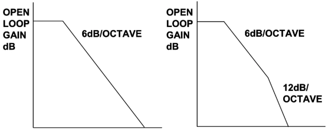
Open-Loop Gain
The open-loop gain (usually referred to as AVOL) is the gain of the amplifier without the feedback loop being closed, hence the name “open-loop.” For a precision op amp this gain can be vary high, on the order of 160 dB or more. This is a gain of 100 million. This gain is flat from dc to what is referred to as the dominant pole. From there it falls off at 6 dB/octave or 20 dB/decade. (An octave is a doubling in frequency and a decade is X10 in frequency). This is referred to as a single-pole response. It will continue to fall at this rate until it hits another pole in the response. This 2nd pole will double the rate at which the open-loop gain falls, that is, to 12 dB/octave or 40 dB/decade. If the open-loop gain has dropped below 0 dB (unity gain) before it hits the 2nd pole, the op amp will be unconditional stable at any gain. This will be typically referred to as unity gain stable on the data sheet. If the 2nd pole is reached while the loop gain is greater than 1 (0 dB), then the amplifier may not be stable under some conditions.
Figure 1.7: Open-Loop Gain (Bode Plot)
It is important to understand the differences between open-loop gain, closed-loop gain, loop gain, signal gain, and noise gain. They are similar in nature, interrelated, but different. We will discuss them all in detail.
The open-loop gain is not a precisely controlled spec. It can, and does, have a relatively large range and will be given in the specs as a typical number rather than a min/max number, in most cases. In some cases, typically high precision op amps, the spec will be a minimum.
In addition, the open-loop gain can change due to output voltage levels and loading. There is also some dependency on temperature. In general, these effects are of a very
OPEN LOOP GAIN dB OPEN LOOP GAIN dB 6dB/OCTAVE 6dB/OCTAVE 12dB/ OCTAVE OPEN LOOP GAIN dB OPEN LOOP GAIN dB 6dB/OCTAVE 6dB/OCTAVE 12dB/ OCTAVE
minor degree and can, in most cases, be ignored. In fact this nonlinearity is not always included in the data sheet for the part.
Figure 1.8: Gain Definition
IN
A
B
C
R1 R2 IN R1 R2 R2 R1 IN Signal Gain = 1 + R2/R1 Noise Gain = 1 + R2/R1 Signal Gain =- R2/R1 Noise Gain = 1 + R2/R1 Signal Gain =- R2/R1 Noise Gain = 1 + R2 Voltage Noise and Offset Voltage of the op amp are reflected to the output by the Noise Gain.
Noise Gain, not Signal Gain, is relevant in assessing stability.
Circuit C has unchanged Signal Gain, but higher Noise Gain, thus better stability, worse noise, and higher output offset voltage. IN
A
B
C
R1 R2 IN R1 R2 R2 R1 IN Signal Gain = 1 + R2/R1 Noise Gain = 1 + R2/R1 Signal Gain = R2/R1 Noise Gain = 1 + R2/R1 Signal Gain = Noise Gain = 1 + R2 INA
B
C
R1 R2 IN R1 R2 R2 R1 IN Signal Gain = 1 + R2/R1 Noise Gain = 1 + R2/R1 Signal Gain =- R2/R1 Noise Gain = 1 + R2/R1 Signal Gain =- R2/R1 Noise Gain = 1 + R2 INA
B
C
R1 R2 IN R1 R2 R2 R1 IN Signal Gain = 1 + R2/R1 Noise Gain = 1 + R2/R1 Signal Gain = R2/R1 Noise Gain = 1 + R2/R1 Signal Gain = Noise Gain = 1 + R2 INA
B
C
R1 R2 IN R1 R2 R2 R1 IN Signal Gain = 1 + R2/R1 Noise Gain = 1 + R2/R1 Signal Gain =- R2/R1 Noise Gain = 1 + R2/R1 Signal Gain =- R2/R1 Noise Gain = 1 + R2 Voltage Noise and Offset Voltage of the op amp are reflected to the output by the Noise Gain.
Noise Gain, not Signal Gain, is relevant in assessing stability.
Circuit C has unchanged Signal Gain, but higher Noise Gain, thus better stability, worse noise, and higher output offset voltage. IN
A
B
C
R1 R2 IN R1 R2 R2 R1 IN Signal Gain = 1 + R2/R1 Noise Gain = 1 + R2/R1 Signal Gain = R2/R1 Noise Gain = 1 + R2/R1 Signal Gain = Noise Gain = 1 + R2 INA
B
C
R1 R2 IN R1 R2 R2 R1 IN Signal Gain = 1 + R2/R1 Noise Gain = 1 + R2/R1 Signal Gain =- R2/R1 Noise Gain = 1 + R2/R1 Signal Gain =- R2/R1 Noise Gain = 1 + R2 INA
B
C
R1 R2 IN R1 R2 R2 R1 IN Signal Gain = 1 + R2/R1 Noise Gain = 1 + R2/R1 Signal Gain = R2/R1 Noise Gain = 1 + R2/R1 Signal Gain = Noise Gain = 1 + R2 + – + – + – R1| | R3Figure 1.9: Noise Gain CLOSED LOOP GAIN NOISE GAIN
GAIN dB
LOG f fCL
LOOP GAIN OPEN LOOP GAIN
CLOSED LOOP GAIN NOISE GAIN GAIN
dB
LOG f fCL
LOOP GAIN OPEN LOOP GAIN
NOISE GAIN GAIN dB LOG f fCL LOOP GAIN OPEN LOOP GAIN
Gain-Bandwidth Product
The open-loop gain falls at 6 dB/octave. This means that if we double the frequency, the gain falls to half of what it was. Conversely, if the frequency is halved, the open-loop gain will double, as shown in Figure 1.8. This gives rise to what is known as the Gain-Bandwidth Product. If we multiply the open-loop gain by the frequency the product is always a constant. The caveat for this is that we have to be in the part of the curve that is falling at 6 dB/octave. This gives us a convenient figure of merit with which to determine if a particular op amp is useable in a particular application.
For example, if we have an application with which we require a gain of 10 and a bandwidth of 100 kHz, we require an op amp with, at least, a gain-bandwidth product of 1 MHz. This is a slight oversimplification. Because of the variability of the gain-bandwidth product, and the fact that at the location where the closed-loop gain intersects the open-loop gain the response is actually down 3 dB, a little margin should be included. In the application described above, an op amp with a gain-bandwidth product of 1 MHz would be marginal. A safety factor of at least 5 would be better insurance that the expected performance is achieved.
Figure 1.10: Gain-Bandwidth Product
Stability Criteria
Feedback theory states that the closed-loop gain must intersect the open-loop gain at a rate of 6 dB/octave (single-pole response) for the system to be stable. If the response is 12 dB/octave (2 pole response) the op amp will oscillate. The easiest way to think of this is that each pole adds 90° of phase shift. Two poles then means 180°, and 180° of phase shift turns negative feedback into positive feedback, which means oscillations.
GAIN
dB OPEN LOOP GAIN, A(s)
IF GAIN BANDWIDTH PRODUCT = X THEN Y ·fCL= X fCL= XY WHERE fCL= CLOSED-LOOP BANDWIDTH LOG f fCL NOISE GAIN = Y Y = 1 + R2 R1 GAIN
dB OPEN LOOP GAIN, A(s)
IF GAIN BANDWIDTH PRODUCT = X THEN Y ·fCL= X fCL= XY WHERE fCL= CLOSED-LOOP BANDWIDTH LOG f fCL NOISE GAIN = Y Y = 1 + R2 R1
The question could be then, why would you want an amplifier that is not unity gain stable? The answer is that for a given amplifier, the bandwidth can be increased if the amplifier is not unity gain stable. This is sometimes referred to as decompensated, But the gain criteria must be met. This criteria is that the closed-loop gain must intercept the open-loop gain at a slope of 6 dB/oct. (single-pole response). If not, the amplifier
will oscillate.
As an example, compare the open-loop gain graphs in Figures 1.11, 1.12, 1.13. The three parts shown, the AD847, AD848, and AD849, are basically the same part. The AD847 is unity gain stable. The AD848 is stable for gains of 2 or more. The AD849 is stable for a gain of 10 or more. You can see from this that the AD849 is much wider bandwidth. So, if you are going to run at high gain, you get wider bandwidth.
There are a couple of tricks that you can use to help out in this regard in the circuit tricks section, which we will cover later.
Figure 1.11: AD847 Open Loop Gain Figure 1.12: AD848 Open Loop Gain
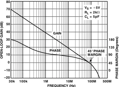
Phase Margin
One measure of stability is phase margin. Just as the amplitude response doesn’t stay flat and then change instantaneously, the phase will also change gradually, starting as much as a decade back from the corner frequency. Phase margin is the amount of phase shift that is left until you hit 180° measured at the unity gain point.
The manifestation of low phase margin is an increase in the peaking of the output just before the close-loop gain intersects the open-loop gain. See Figure 1.14.
Figure 1.14: AD8051 Phase Margin
Closed-Loop Gain
This, of course, is the gain of the amplifier with the feedback loop closed, as opposed the open-loop gain, which is the gain with the feedback loop opened. It has two forms, signal gain and noise gain. These are described and differentiated below.
The expression for the gain of a closed-loop amplifier involves the open-loop gain. If G is the actual gain, NG is the noise gain (see below), and AVOL is the open-loop gain of the amplifier, then:
From this you can see that if the open-loop gain is very high, which it typically is, the closed-loop gain of the circuit is simply the noise gain.
G NG NG NG = -+ 2 NG NG A AVOL G NG NG NG = -+ = 2 NG NG AVOL NG NG A + 1 A G NG NG NG = -+ 2 NG NG A AVOL G NG NG NG = -+ = 2 NG NG AVOL NG NG A + 1 A Eq. 1-9 80 40 –10 70 60 50 30 20 10 0 –20 30k 100k 1M 10M 100M GAIN PHASE 45° PHASE MARGIN VS =+5V RL = 2kΩ CL = 5pF FREQUENCY (Hz) 180 135 90 45 0 500M OP E N -L OOP GA IN ( d B ) P H A S E M A R G IN ( D e g rees)
Signal Gain
This is the gain applied to the input signal, with the feedback loop connected. In the basic operation section above, when we talked about the gain of the inverting and noninverting circuits, we were actually more correctly talking about the closed-loop signal gain. It can be inverting or noninverting. It can even be less than unity for the inverting case. Signal gain is the gain that we are primarily interested in when designing circuits.
The signal gain for an inverting amplifier stage is:
and for a noninverting amplifier it is:
Noise Gain
Noise gain is the gain applied to a noise source in series with an op amp input. It is also the gain applied to an offset voltage. The noise gain is equal to:
Noise gain is equal to the signal gain of a noninverting amp. It is the same for either an inverting or noninverting stage.
It is the noise gain that is used to determine stability. It is also the closed-loop gain that is used in Bode plots. Remember that even though we used resistances in the equation for noise gain, they are actually impedances.
R in R fb = 1+ A R in R in R fb R fb = 1+ A R in R fb = 1+ A R in R in R fb R fb = 1+ A R in R in R fb R fb = 1+ A R in R in R fb R fb = 1+ A = 1+ R fbR fb A A = Rfb R in
-A = Rfb R in Rfb R in -A = Rfb R in -A = Rfb R in Rfb R in-
Eq. 1-10 Eq. 1-11 Eq. 1-12IN
A
B
C
R1 R2 IN R1 R2 R2 R1 IN Signal Gain = 1 + R2/R1 Noise Gain = 1 + R2/R1 Signal Gain = - R2/R1 Noise Gain = 1 + R2/R1 Signal Gain = - R2/R1 Noise Gain = 1 + R2 R Voltage Noise and Offset Voltage of the op amp are reflected tothe output by the Noise Gain.
Noise Gain, not Signal Gain, is relevant in assessing stability. Circuit C has unchanged Signal Gain, but higher Noise Gain, thus
better stability, worse noise, and higher output offset voltage.
IN
A
B
C
R1 R2 IN R1 R2 R2 R1 IN Signal Gain = 1 + R2/R1 Noise Gain = 1 + R2/R1 Signal Gain = R2/R1 Noise Gain = 1 + R2/R1 Signal Gain = Noise Gain = 1 + R2 Voltage Noise and Offset Voltage of the op amp are reflected tothe output by the Noise Gain.
Noise Gain, not Signal Gain, is relevant in assessing stability. Circuit C has unchanged Signal Gain, but higher Noise Gain, thus
better stability, worse noise, and higher output offset voltage.
IN
A
B
C
R1 R2 IN R1 R2 R2 R1 IN Signal Gain = 1 + R2/R1 Noise Gain = 1 + R2/R1 Signal Gain = - R2/R1 Noise Gain = 1 + R2/R1 Signal Gain = - R2/R1 Noise Gain = 1 + R2 R1| | R3 Voltage Noise and Offset Voltage of the op amp are reflected tothe output by the Noise Gain.
Noise Gain, not Signal Gain, is relevant in assessing stability. Circuit C has unchanged Signal Gain, but higher Noise Gain, thus
better stability, worse noise, and higher output offset voltage.
IN
A
B
C
R1 R2 IN R1 R2 R2 R1 IN Signal Gain = 1 + R2/R1 Noise Gain = 1 + R2/R1 Signal Gain = R2/R1 Noise Gain = 1 + R2/R1 Signal Gain = Noise Gain = 1 + R2 Voltage Noise and Offset Voltage of the op amp are reflected tothe output by the Noise Gain.
Noise Gain, not Signal Gain, is relevant in assessing stability. Circuit C has unchanged Signal Gain, but higher Noise Gain, thus
better stability, worse noise, and higher output offset voltage.
+ – + – + –
Figure 1.15: Noise Gain
Loop Gain
The difference between the open-loop gain and the closed-loop gain is known as the loop gain. This is useful information because it gives you the amount of negative feedback that can apply to the amplifier system.
Figure 1.16: Gain Definitions
NOISE GAIN GAIN dB LOG f fCL LOOP GAIN OPEN LOOP GAIN
CLOSED LOOP GAIN NOISE GAIN GAIN
dB
LOG f fCL
LOOP GAIN OPEN LOOP GAIN
Bode Plot
The plotting of open-loop gain vs. frequency on a log-log scale gives is what is known as a Bode (pronounced boh dee) plot. It is one of the primary tools in evaluating whether a particular op amp is suitable for a particular application.
If you plot the open-loop gain and then the noise gain on a Bode plot, the point where they intersect will determine the maximum closed-loop bandwidth of the amplifier system. This is commonly referred to as the closed-loop frequency (FCL). Remember that the true response at the intersection is actually 3 dB down. One octave above and one octave below FCL the difference between the asymptotic response and the real response will be less than 1 dB.
Figure 1.17: Asymptotic Response
The Bode plot is also useful in determining stability. As stated above, if the closed-loop gain (noise gain) intersects the open-loop gain at a slope of greater than 6 dB/octave (20 dB/decade) the amplifier may be unstable (depending on the phase margin).
GA IN FREQUENCY 0 10 20 30 40 FCL
NOISE GAIN OPEN LOOP GAIN
GA IN FREQUENCY 0 10 20 30 40 FCL NOISE GAIN
Current Feedback (CFB) Model
There is a type of amplifier that have several advantages over the standard VFB amplifier at high frequencies. They are called current feedback (CFB) or sometimes transimpedance amps. There is a possible point of confusion since the current–to-voltage (I/V) converters commonly found in photodiode applications are also referred to as transimpedance amps. Schematically CFB op amps look similar to standard VFB amps, but there are several key differences.
The input structure of the CFB is different from the VFB. While we are trying not to get into the internal structures of the op amps, in this case, a simple diagram is in order. See Figure 1.18. The mechanism of feedback is also different, hence the names. But again, the exact mechanism is beyond what we want to cover here. In most cases if the differences are noted, and the attendant limitations observed, the basic operation of both types of amplifiers can be thought of as the same. The gain equations are the same as for a VFB amp, with an important limitation as noted in the next section.
Figure 1.18: VFB and CFB Amplifiers
Difference from VFB
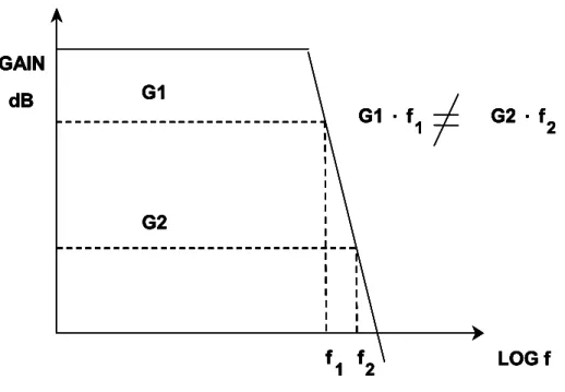
One primary difference between the CFB and VFB amps is that there is not a Gain-Bandwidth product. While there is a change in bandwidth with gain, it is not even close to the 6 dB/octave that we see with VFB. See Figure 1.19. Also, a major limitation that the value of the feedback resistor determines the bandwidth, working with the internal capacitance of the op amp. For every CFB op amp there is a recommended value of feedback resistor for maximum bandwidth. If you increase the value of the resistor, you reduce the bandwidth. If you use a lower value of resistor the phase margin is reduced and the amplifier could become unstable. This optimum value of resistor is different for different operational conditions. For instance, the value will change for different packages, for example, SOIC vs. DIP (see Figure 1.20).
~
+
– v
–A(s) v
A(s) = OPEN LOOP GAIN VOUT= A(s)*v R2 R1 VIN + – i –T(s) i T(s) RO i ×1 R2 R1 VIN VOUT ×1
T(s) = TRANSIMPEDANCE OPEN LOOP GAIN VOUT= -T(s)*i VOUT
~
+ – v –A(s) vA(s) = OPEN LOOP GAIN VOUT= A(s)*v R2 R1 VIN + – i –T(s) i T(s) RO i ×1 R2 R1 VIN VOUT ×1
T(s) = TRANSIMPEDANCE OPEN LOOP GAIN VOUT= -T(s)*i
Figure 1.19: Current Feedback Amplifier Frequency Response Component RF (Ω) RG (Ω) RO (Nominal) (Ω) RS (Ω) RT (Nominal) (Ω) Small Signal –1 649 649 49.9 0 54.9 340 +1 1050 49.9 49.9 880 +2 750 750 49.9 49.9 460 +10 470 51 49.9 49.9 260 +100 1000 10 49.9 49.9 20 AD8001AN (PDIP) Gain –1 604 604 49.9 0 54.9 370 +1 953 49.9 49.9 710 +2 681 681 49.9 49.9 440 +10 470 51 49.9 49.9 260 +100 1000 10 49.9 49.9 20 AD8001AR (SOIC) Gain –1 845 845 49.9 0 54.9 240 +1 1000 49.9 49.9 795 +2 768 768 49.9 49.9 380 +10 470 51 49.9 49.9 260 +100 1000 10 49.9 49.9 20 AD8001ART (SOT-23-5) Gain (MHz) BW (MHz) 0.1 db Flatness 105 70 105 130 100 120 110 300 145
Figure 1.20: AD8001 Optimum Feedback Resistor vs. Package
Also, a CFB amplifier should not have a capacitor in the feedback loop. If a capacitor is used in the feedback loop, it reduces the feedback impedance as frequency is increased, which will cause the op amp to oscillate. You need to be careful of stray capacitances around the inverting input of the op amp for the same reason.
A common error in using a current feedback op amp is to short the inverting input directly to the output in an attempt to build a unity gain voltage follower (buffer). This circuit will oscillate. Obviously, in this case, the feedback resistor value will be less the recommended value. The circuit is perfectly stable if the recommended feedback resistor of the correct value is used in place of the short.
Another difference between the VFB and CFB amplifiers is that the inverting input of the CFB amp is low impedance. By low we mean typically 50 Ω to 100 Ω. Therefore there FEEDBACK RESISTOR FIXED FOR OPTIMUM PERFORMANCE. LARGER VALUES
REDUCE BANDWIDTH, SMALLER VALUES MAY CAUSE INSTABILITY.
FOR FIXED FEEDBACK RESISTOR, CHANGING GAIN HAS LITTLE EFFECT ON BANDWIDTH.
CURRENT FEEDBACK OP AMPS DO NOT HAVE A FIXED GAIN -PRODUCT. GAIN dB G1 G2 G1 ·f1 G2 ·f2 f1 f2 LOG f
FEEDBACK RESISTOR FIXED FOR OPTIMUM PERFORMANCE. LARGER VALUES REDUCE BANDWIDTH, SMALLER VALUES MAY CAUSE INSTABILITY.
FOR FIXED FEEDBACK RESISTOR, CHANGING GAIN HAS LITTLE EFFECT ON BANDWIDTH.
CURRENT FEEDBACK OP AMPS DO NOT HAVE A FIXED GAIN-- BANDWIDTH PRODUCT. GAIN dB G1 G2 G1 ·f1 G2 ·f2 f1 f2 LOG f GAIN dB G1 G2 G1 ·f1 G2 ·f2 f1 f2 LOG f
Slew rate performance is also enhanced by the CFB topology. The current that is available to charge the internal compensation capacitor is dynamic. It is not limited to any fixed value as is often the case in VFB topologies. With a step input or overload condition, the current is increased (current-on-demand) until the overdriven condition is removed. The basic current feedback amplifier has no fundamental slew-rate limit. Limits only come about from parasitic internal capacitances and many strides have been made to reduce their effects.
The combination of higher bandwidths and slew rate allows CFB devices to have good distortion performance while doing so at a lower power.
The distortion of an amplifier is impacted by the open loop distortion of the amplifier and the loop gain of the closed-loop circuit. The amount of open-loop distortion contributed by a CFB amplifier is small due to the basic symmetry of the internal topology. Speed is the other main contributor to distortion. In most configurations, a CFB amplifier has a greater bandwidth than its VFB counterpart. So at a given signal frequency, the faster part has greater loop-gain and therefore lower distortion.
How to Choose Between CFB and VFB
The application advantages of current feedback and voltage feedback differ. In many applications, the differences between CFB and VFB are not readily apparent. Today’s CFB and VFB amplifiers have comparable performance, but there are certain unique advantages associated with each topology. Voltage feedback allows freedom of choice of the feedback resistor (or impedance) at the expense of sacrificing bandwidth for gain. Current feedback maintains high bandwidth over a wide range of gains at the cost of limiting the choices in the feedback impedance.
In general, VFB amplifiers offer: • Lower Noise
• Better DC Performance
• Feedback Component Freedom while CFB amplifiers offer:
• Faster Slew Rates • Lower Distortion
• Feedback Component Restrictions
Supply Voltages
Historically the supply voltage for op amps was typically ±15 V. The operational input and output range was on the order of ±10 V. But there was no hard requirement for these levels. Typically the maximum supply was ±18 V. The lower limit was set by the internal structures. You could typically go within 1.5 or 2 V of either supply rail, so you could reasonably go down to ±8 V supplies or so and still have a reasonable dynamic range.
Lately though, there has been a trend toward lower supply voltages. This has happened for a couple of reasons.
First, high speed circuits typically have a lower full scale range. The principal reason for this is the amplifiers ability to swing large voltages. All amplifiers have a slew rate limit, which is expressed as so many volts per microsecond. So if you want to go faster, your voltage range must be reduced, all other things being equal. A second reason is that to limit the effects of stray capacitance on the circuits, you need to reduce their impedance levels. Driving lower impedances increases the demands on the output stage, and on the power dissipation abilities of the amplifier package. Lower voltage swings require lower currents to be supplied, thereby lowering the dissipation of the package.
A second reason is that as the speed of the devices inside the amplifier increased, the geometries of these devices tend to become smaller. The smaller geometries typically mean reduced breakdown voltages for these parts. Since the breakdown voltages were getting lower, the supply voltages had to follow. Today high speed op amps typically have breakdown voltage of ±7 V, and so the supplies are typically ±5 V, or even lower. In some cases, operation on batteries established a requirement for lower supply voltages. Lower supplies would then lessen the number of batteries, which, in turn, reduced the size, weight and cost of the end product.
At the same time there was a movement towards single supply systems. Instead of the typical plus and minus supplies, the op amps operate on a single positive supply and ground, the ground then becoming the negative supply.
Single Supply Considerations
There is nothing in the circuitry of the op amp that requires ground. In fact, instead of a bipolar (+ and −) supply of ±15 V you could just as easily use a single supply of +30 V (ground being the negative supply), as long as the rest of the circuit was biased correctly so that the signal was within the common mode range of op amp. Or, for that matter, the supply could just as easily be –30 V (ground being the most positive supply).
When you combine the single supply operation with reduced supply voltages you can run into problems. The standard topology for op amps uses a NPN differential pair (see Figure 1.21) for the input and emitter followers (see Figure 1.24) for the output stage. Neither of these circuits will let you run “rail-to-rail,” that is from one supply to the other. Some circuit modifications are required.
The first of these modifications was the use of a PNP differential input See Figure 1.22. One of the first examples of this input configuration was the LM324. This configuration allowed the input to get close to the negative rail (ground). It could not, however, go to the positive rail. But in many systems, especially mixed signal systems that were predominately digital, this was enough. In terms of precision, the 324 is not a stellar performer.
Figure 1.21: Standard Input Stage (Differential Pair)
The NPN input cannot swing to ground. The PNP input can not swing to the positive rail. The next modification was to use a dual input. Here a NPN differential pair is combined with a PNP differential pair. See Figure 1.23. Over most of the common-mode range of the input both pairs are active. As one rail or the other is approached, one of the inputs turns off. The NPN pair swings to the upper rail and the PNP pair swings to the lower rail.
.
Figure 1.22: PNP Input Stage
It should be noted here that the op amp parameters which primarily depend on the input structure (bias current, for instance) will vary with the common-mode voltage on the inputs. The bias currents will even change direction as the front end transitions from the NPN stage to the PNP stage.
Another difference is the output stage. The standard output stage, which is a complimentary emitter follower (common collector) configuration (Figure 1.24), is
VIN VIN +VS -VS +VS -VS
typically replaced by a common emitter circuit. This allows the output to swing close to the rails. The exact level is set by the VCEsat of the output transistors, which is, in turn,
dependent on the output current levels. The only real disadvantage to this arrangement is that the output impedance of the common emitter circuit is higher than the common collector circuit. Most of the time this is not really an issue, since negative feedback reduces the output impedance proportional to the amount of loop gain. Where it becomes an issue is that as the loop gain falls this higher output impedance is more susceptible to the effects of capacitate loading.
Figure 1.23: Compound input Stage
Figure 1.24: Output Stages. Emitter Follower for Standard Configuration And Common Emitter for “Rail-to-Rail” Configuration
+VS
-VS +VS
-VS
+VS
EMITTER FOLLOWER COMMON EMITTER
+VS
-VS -VS
Circuit Design Considerations for Single Supply Systems
Many waveforms are bipolar in nature. This means that the signal naturally swings around the reference level, which is typically ground. This obviously won’t work in a single-supply environment. What is required is to ac couple the signals.
Figure 1.25: Single Supply Biasing
AC coupling is simply applying a high-pass filter and establishing a new reference level typically somewhere around the center of the supply voltage range. See Figure 1.25. The series capacitor will block the dc component of the input signal. The corner frequency (the frequency at which the response is 3 dB down from the midband level) is determined by the value of the components:
where:
It should be noted that if multiple sections are ac coupled, each section will be 3 dB down at the corner frequency. So if there are two sections with the same corner frequency, the total response will be 6 dB down, three sections would be 9 dB down, etc. This should be taken into account so that the overall response of the system will be adequate. Also keep in mind that the amplitude response starts to roll off a decade, or more, from the corner frequency. 1 2πREQC fC = 1 2πREQC fC = 649Ω VLOAD
-+
U1 47μF R1 649Ω = +5V VIN 4.99kΩ R3 4.99kΩ + CIN R4 C2 R5 R2 C1 + + 220μF 10μF VS + + 0.1μF 100μF/25V C2 1μF 1000μF COUT 75Ω RL C4 C3 10k Ω 649Ω VLOAD-+
U1 47μF R1 649Ω = +5V VIN 4.99kΩ R3 4.99kΩ + CIN R4 C2 R5 R2 C1 + + 220μF 10μF VS + + 0.1μF 100μF/25V C2 1μF 1000μF COUT 75Ω RL C4 C3 649Ω VLOAD-+
U1 47μF R1 649Ω = +5V VIN 4.99kΩ R3 4.99kΩ + CIN R4 C2 R5 R2 C1 + + 220μF 10μF VS + + 0.1μF 100μF/25V C2 1μF 1000μF COUT 75Ω RL C4 C3 10k Ω R4 R5 R4 + R5 REQ == R4 + R5R4 + R5R4 R5R4 R5 REQ == R4 + R5R4 R5 Eq. 1-14 Eq. 1-15The AC coupling of arbitrary waveforms can actually introduce problems which don’t exist at all in dc coupled systems. These problems have to do with the waveform duty cycle, and are particularly acute with signals which approach the rails, as they can in low supply voltage systems which are ac coupled.
Fig. 1.26: Headroom Issues with Single-Supply Biasing
In an amplifier circuit such as that of Figure 1.25, the output bias point will be equal to the dc bias as applied to the op amp’s (+) input. For a symmetric (50% duty cycle) waveform of a 2 V p-p output level, the output signal will swing symmetrically about the bias point, or nominally 2.5 V ±1 V (using the values give in Fig. 1.25). If, however, the pulsed waveform is of a very high (or low) duty cycle, the ac averaging effect of CINand R4 || R5will shift the effective peak level either high or low, dependent upon the duty cycle. This phenomenon has the net effect of reducing the working headroom of the amplifier, and is illustrated in Figure 1.26.
In Figure 1.26 (A), an example of a 50% duty cycle square wave of about 2 V p-p level is shown, with the signal swing biased symmetrically between the upper and lower clip points of a 5 V supply amplifier. This amplifier, for example, (an AD817 biased similarly to Figure 1.25) can only swing to the limited dc levels as marked, about 1 V from either rail. In cases (B) and (C), the duty cycle of the input waveform is adjusted to both low and high duty cycle extremes while maintaining the same peak-to-peak input level. At the amplifier output, the waveform is seen to clip either negative or positive, in (B) and (C), respectively. (A) 50% DUTY CYCLE NO CLIPPING (B) LOW DUTY CYCLE CLIPPED POSITIVE (C) HIGH DUTY CYCLE CLIPPED NEGATIVE 2Vp-p 2Vp-p 2Vp-p 4.0V (+) CLIPPING 2.5V 1.0V (-) CLIPPING 4.0V (+) CLIPPING 2.5V 1.0V (-) CLIPPING 4.0V (+) CLIPPING 2.5V 1.0V (-) CLIPPING
Rail-to-Rail
When the input and/or the output can swing very close to the supply rails, it is referred to as “rail-to-rail.” There is no industry standard definition for this. At Analog Devices we have defined this at swinging to within 100 mV of either rail. For the output this is driving a standard load, since the actual maximum output level will depend on the output current. Note that not all amplifiers that are touted as single supply are rail-to-rail. And not all rail-to-rail amplifiers are rail-to-rail on input and output. It could be one or the other, or both, or neither. The bottom line is that you must read the data sheet. In no case can the output actually swing completely to the rails.
Phase Reversal
There is an interesting phenomenon that can occur when the common-mode range of the op amp is exceeded. Some internal nodes can turn off and the output will be pulled to the opposite rail until the input comes back into the operational range. Many modern designs take steps to eliminate this problem. Many times this is called out in the bullets on the cover page. See Figure 1.27. Phase reversal is most common when the amplifier us in the follower mode.
Figure 1.27: Phase Reversal
Low Power and Micropower
Along with the trend toward single supplies is the trend toward lower quiescent power. This is the power used by the amp itself. We have arrived at the point where there are whole amplifiers that can operate on the bias current of the 741.
One way to lower the quiescent power is to lower the bias current in the output stage. This amounts to moving more towards class B operation (and away from class A). The result of this is that the distortion of the output stage will tend to rise.
Another approach to lower power is to lower the standing current of the input stage. The result of this is to reduce the bandwidth and to increase the noise.
While the term “low power” can mean vastly different things depending on the application. At Analog Devices we have set a definition for op amps. Low power means the quiescent current is less than 1 mA per amplifier. Micropower is defined as having a quiescent current less than 100 μA per amplifier. As was the case with “rail-to-rail,” this is not an industry wide definition.
Processes
The vast majority of modern op amps are built using bipolar transistors.
Occasionally a junction FET is used for the input stage. This is commonly referred to as a Bi-Fet (for Bipolar-FET). This is typically done to increase the input impedance of the op amp, or conversely, to lower the input bias currents. The FET devices are typically used only in the input stage. For single-supply applications, the FETs can be either N-channel or P-channel. This allows input ranges extending to the negative rail and positive rail, respectively.
CMOS processing is also used for op amps. While historically CMOS hasn’t been that attractive a process for linear amplifiers, process and circuit design have progressed to the point that quite reasonable performance can be obtained from CMOS op amps.
One particularly attractive aspect of using CMOS is that it lends itself easily to mixed mode (analog and digital) applications. Some examples of this are the Digi-Trim and chopper stabilized op amps.
“Digi-Trim” is a technique that allows the offset voltage of op amps to be adjusted out at final test. This replaces the more common techniques of zener-zapping or laser trimming, which must be done at the wafer level. The problem with trimming at the wafer level is that there are certain shifts in parameters due to packaging, etc., that take place after the trimming is done. While the shift in parameters is fairly well understood and some of the shift can be anticipated, trimming at final test is a very attractive alternative. The Digi-trim amplifiers basically incorporate a small DAC used to adjust the offset.
Chopper stabilized amplifiers use techniques to adjust out the offset continuously. This is accomplished by using a dc precision amp to adjust the offset of a wider bandwidth amp. The dc precision amp is switched between a reference node (usually ground) and the input. This then is used to adjust the offset of the “main” amp.
Effects of Overdrive on Op Amp Inputs
There are several important points to be considered about the effects of overdrive on op amp inputs. The first is, obviously, damage. The data sheet of an op amp will give “absolute maximum” input ratings for the device. These are typically expressed in terms of the supply voltage but, unless the data sheet expressly says otherwise, maximum ratings apply only when the supplies are present, and the input voltages should be held near zero in the absence of supplies.
A common type of rating expresses the maximum input voltage in terms of the supply, Vss ± 0.3 V. In effect, neither input may go more than 0.3 V outside the supply rails, whether they are on or off. If current is limited to 5 mA or less, it generally does not matter if inputs do go outside ±0.3 V when the supply is off (provided that no base-emitter reverse breakdown occurs). Problems may arise if the input is outside this range when the supplies are turned on as this can turn on parasitic SCRs in the device structure and destroy it within microseconds. This condition is called latch-up, and is much more common in digital CMOS than in linear processes used for op amps. If a device is known to be sensitive to latch-up, avoid the possibility of signals appearing before supplies are established. (When signals come from other circuitry using the same supply there is rarely, if ever, a problem.) Fortunately, most modern IC op amps are relatively insensitive to latch-up.
Input stage damage will be limited if the input current is limited. The standard rule-of-thumb is to limit the current to 5 mA. Reverse bias junction breakdown should be avoided at all cost. Note that the common-mode and differential-mode specs may be different. Also, not all overvoltage damage is catastrophic. Small degradation of some of the specs can occur with constant abuse by overvoltaging the op amp.
A common method of keeping the signal within the supplies is to clamp the signal to the supplies with Schottky diodes as shown in Figure 1.28. This does not, in fact, limit the signal to ±0.3 V at all temperatures, but if the Schottky diodes are at the same temperature as the op amp, they will limit the voltage to a safe level, even if they do not limit it at all times to within the data sheet rating. This is easily accomplished if overvoltage is only possible at turn-on, and diodes and op amp will always be at the same temperature then. If the op amp may still be warm when it is repowered, however, steps must be taken to ensure that diodes and op amp are at the same temperature when this occurs.
Many op amps have limited common-mode or differential input voltage ratings. Limits on common-mode are usually due to complex structures in very fast op amps and vary from device to device. Limits on differential input avoid a damaging reverse breakdown of the input transistors (especially super-beta transistors). This damage can occur even at very low current levels. Limits on differential inputs may also be needed to prevent internal protective circuitry from over-heating at high current levels when it is conducting to prevent breakdowns—in this case, a few hundred microseconds of overvoltage may do no harm. One should never exceed any “absolute maximum” rating, but engineers should
understand the reasons for the rating so that they can make realistic assessments of the risk of permanent damage should the unexpected occur.
If an op amp is overdriven within its ratings, no permanent damage should occur, but some of the internal stages may saturate. Recovery from saturation is generally slow, except for certain “clamped” op amps specifically designed for fast over-drive recovery. Over-driven amplifiers may therefore be unexpectedly slow.
Because of this reduction in speed with saturation (and also output stages unsuited to driving logic), it is generally unwise to use an op amp as a comparator. Nevertheless, there are sometimes reasons why op amps may be used as comparators. The subject is discussed in Reference 3 and Chapter 2.
Figure 1.28: Input Overvoltage Protection
+VS -VS RS + -+VS -VS RS +
-SECTION 2: OP AMP SPECIFICATIONS
Introduction
In this section, we will discuss basic op amp specs. The importance of any of these specs depends, of course, upon the application. For instance, offset voltage, offset voltage drift, and open-loop gain (dc specs) are very critical in precision sensor signal conditioning circuits, but may not be as important in high speed applications where bandwidth, slew rate, and distortion (ac specs) are typically the key specs.
Most op amp specs are largely topology independent. However, although voltage feedback (VFB) and current feedback (CFB) op amps have similar error terms and specs, the application of each part warrants discussing some of the specs separately. In the following discussions, this will be done where significant differences exist.
It should be noted that not all of these specs will necessarily appear on all data sheets. As the performance of the op amp increases, the more specs it has and the tighter the specs become. Also keep in mind the difference between typical and min/max. At Analog Devices, a spec that is min/max is guaranteed by test. Typ specs are generally not tested.
DC Specifications
Open-Loop Gain
The open-loop gain is the gain of the amplifier when the feedback loop is not closed. It is generally measured, however, with the feedback loop closed, although at a very large gain. In an ideal op amp, it is infinite with infinite bandwidth. In practice, it is very large (up to 160 dB) at dc. At some frequency (the dominant pole) it starts to fall at
6 dB/octave or 20 dB/decade. (An octave is a doubling in frequency and a decade is ×10 in frequency). This is referred to as a single-pole response. The dominant pole frequency will range from in the neighborhood of 10 Hz for some high precision amps to several kHz for some high speed amps. It will continue to fall at this rate until it reaches another pole in the response. This 2nd pole will double the rate at which the open-loop gain falls, that is to 12 dB/octave or 40 dB/decade. If the open-loop gain has gone below 0 dB (unity gain) before the amp hits the 2nd pole, the op amp will be unconditionally stable at any gain. This will be referred to as unity gain stable on the data sheet. If the 2nd pole is reached while the loop gain is greater than 1 (0 db), then the amplifier may not be stable under some conditions.
Figure. 1.29: Open-Loop Gain
Since the open-loop gain falls by half with a doubling of frequency with a single pole response, there is what is called a constant gain-bandwidth product. At any point along the curve, if the frequency is multiplied by the gain at that frequency, the product is a constant. For example, if an amplifier has a 1 MHz gain bandwidth product, the open-loop gain will be 10 (20 dB) at 100 kHz, 100 (40 dB) at 10 kHz, etc. This is readily apparent on a Bode plot, which plots gain vs. frequency on a log-log scale.
Since a voltage feedback op amp operates as a voltage in/voltage out device, its open-loop gain is a dimensionless ratio, so no unit is necessary. Data sheets sometimes express gain in V/mV or V/µV instead of V/V, for the convenience of using smaller numbers. Or voltage gain can also be expressed in dB terms, as gain in dB = 20 × logAVOL. Thus an
OPEN LOOP GAIN dB OPEN LOOP GAIN dB 6dB/OCTAVE 6dB/OCTAVE 12dB/ OCTAVE
Single Pole Response Two Pole Response
OPEN LOOP GAIN dB OPEN LOOP GAIN dB 6dB/OCTAVE 6dB/OCTAVE 12dB/ OCTAVE
open-loop gain of 1 V/μV (or 1000 V/mV or 1,000,000 V/V) is equivalent to 120 dB, and so on.
Figure 1.30: Bode Plot (for VFB Amps)
For very high precision work, the nonlinearity of the open-loop gain must be considered. Changes in the output voltage level and output loading are the most common causes of changes in the open-loop gain of op amps. A change in open-loop gain with signal level produces a nonlinearity in the closed-loop gain transfer function, which cannot be removed during system calibration. Most op amps have fixed loads, so AVOL changes with
load are not generally important. However, the sensitivity of AVOL to output signal level
may increase for higher load currents. See Figure 1.31.
Figure 1.31: Open-Loop Nonlinearity
GAIN
dB OPEN LOOP GAIN, A(s)
IF GAIN BANDWIDTH PRODUCT = X THEN Y ·fCL= X fCL= XY WHERE fCL= CLOSED-LOOP BANDWIDTH LOG f fCL NOISE GAIN = Y Y = 1 + R2 R1 GAIN
dB OPEN LOOP GAIN, A(s)
IF GAIN BANDWIDTH PRODUCT = X THEN Y ·fCL= X fCL= XY WHERE fCL= CLOSED-LOOP BANDWIDTH LOG f fCL NOISE GAIN = Y Y = 1 + R2 R1 VY 50mV / DIV. (0.5µV / DIV.) (RTI) VX= OUTPUT VOLTAGE 0 +10V –10V RL= 10kΩ RL= 2kΩ
AVOL (AVERAGE) ≈8 million
AVOL,MAX ≈ 9.1 million, AVOL,MIN ≈ 5.7million OPEN LOOP GAIN NONLINEARITY ≈ 0.07ppm CLOSED LOOP GAIN NONLINEARITY ≈ NG×0.07ppm
AVOL= ΔVX ΔVOS VOS VY 50mV / DIV. (0.5µV / DIV.) (RTI) VX= OUTPUT VOLTAGE 0 +10V –10V RL= 10kΩ RL= 2kΩ
AVOL (AVERAGE) ≈8 million
AVOL,MAX ≈ 9.1 million, AVOL,MIN ≈ 5.7million OPEN LOOP GAIN NONLINEARITY ≈ 0.07ppm CLOSED LOOP GAIN NONLINEARITY ≈ NG×0.07ppm
AVOL= ΔVX
ΔVOS AVOL= ΔVX
ΔVOS
The severity of this nonlinearity varies widely from one device type to another, and generally isn’t specified on the data sheet. The minimum AVOL is always specified, and choosing an op amp with a high AVOL will minimize the probability of gain nonlinearity errors. There is no way to compensate for AVOL nonlinearity.
Open-Loop Transresistance of a CFB Op Amp
For current feedback amplifiers, the open-loop response is voltage out for a current in, so it is a transresistance (expressed in ohms) rather than a gain. This is generally referred to as a transimpedance, since there is an ac component as well as a dc term. The
transimpedance of a CFB amp will usually be in the range of 500 kΩ to 1 MΩ.
A CFB op amp loop transimpedance does not vary in the same way as a VFB open-loop gain. Therefore, a CFB op amp will not have the same gain-bandwidth product as VFB amps. While there is some variation of frequency response with frequency with a CFB amp, it is nowhere near 6 dB/octave. See Figure 1.32.
When using the term transimpedance amplifier, there can be some confusion. An amplifier configured as a current to voltage (I/V) converter, typically in photodiode circuits, is also referred to as a transimpedance amplifier. But the photodiode application will generally use a FET input VFB amp rather than a CFB amp. This is because the current levels in the photodiode applications will be very low, not the most compatible with the low impedance input of a CDB op amp.
Figure 1.32: Open-Loop Gain of a CFB Op Amp GAIN dB G1 G2 G1 · f1 G2 · f2 f1 f2 LOG f GAIN dB G1 G2 G1 · f1 G2 · f2 f1 f2 LOG f GAIN dB G1 G2 G1 · f1 G2 · f2 f1 f2 LOG f GAIN dB G1 G2 G1 · f1 G2 · f2 f1 f2 LOG f GAIN dB G1 G2 G1 · f1 G2 · f2 f1 f2 LOG f GAIN dB G1 G2 G1 · f1 G2 · f2 f1 f2 LOG f
Offset Voltage
If both inputs of an op amp are at exactly the same voltage, then the output should be at zero volts, since a differential of 0 V should produce an output of 0 V. In practice, however, there will typically be some voltage at the output. This is known as the offset voltage or VOS. The typical way to specify offset voltage is as the amount of voltage that
must be added to the input to force 0 V out. This voltage, divided by the noise gain of the circuit, is the input offset voltage or input referred offset voltage. The offset voltage is usually input referred to eliminate the effect of circuit gain, which makes comparisons easier. The offset voltage is modeled as a voltage source, VOS, in series with the inverting
input of the op amp as shown in Figure 1.33 .
Figure 1.33: Offset Voltage
Offset Voltage Drift
The input offset voltage varies with temperature. Its temperature coefficient is known as
TCVOS, or more commonly, drift. Offset drift may be as low as 0.1 µV/ºC (typical value
for OP177F, a very high precision op amp). More typical drift values for a range of general purpose precision op amps lie in the range 1 µV/°C to 10 µV/ºC. Most op amps have a specified value of TCVOS, but some, instead, have a second value of maximum VOS
that is guaranteed over the operating temperature range. Such a spec is less useful, because there is no guarantee that TCVOS is constant or monotonic.
Drift with Time
The offset voltage also changes as time passes, or ages. Aging is generally specified in µV/month or µV/1000 hours, but this can be misleading. Aging is not linear, but instead a nonlinear phenomenon that is proportional to the square root of the elapsed time. A drift rate of 1 µV/1000 hours therefore becomes about 3 µV/year (not 9 µV/year). Long-term drift of the OP177F is approximately 0.3 µV/month. This refers to a time period after the first 30 days of operation. Excluding the initial hour of operation, changes in the offset voltage of these devices during the first 30 days of operation are typically less than 2 µV. The long term drift of offset voltage with time is not always specified, even for precision op amps. -+ VOS -+ VOS -+ VOS -+ VOS
Correction for Offset Voltage
Early op amps typically had pins available for nulling out offset voltages. A potentiometer connected to these pins, and the wiper connected to one or the other of the supply voltages, allowed balancing the input stage, which, in turn, nulled out the offset voltage. See Figure 1.34.
Makers of high precision op amps, such as Analog Devices (ADI) and Precision Monolithics (PMI) employed circuit design tricks to internally balance the input structures. ADI used laser trimming of the input stage load resistors to achieve balance. PMI used a technique call zener zapping to accomplish basically the same thing.
Figure 1.34: Offset Adjustment Pins
Laser trimming used lasers to eat away part of the collector resistors to adjust their value. Zener zapping involved having a string of resistors, each bypassed by a semiconductor structure that is basically a zener diode. By applying a pulse of voltage these zener diodes would be shorted out (zapped). This adjusts the value of the resistor string.
DigiTrim™ Technology
DigiTrim is a technique which adjusts circuit offset performance by programming digitally weighted current sources, in essence a DAC. This technique makes use of the mixed signal capabilities of the CMOS process. While, historically, CMOS would not be the first choice for precision amplifiers, recent process improvements combined with the DigiTrim technology result in a very reasonable precision performance. In this patented new trim method, the trim information is entered through existing analog pins using a special digital keyword sequence. The adjustment values can be temporarily programmed, evaluated and readjusted for optimum accuracy before permanent adjustment is performed. After the trim is completed, the trim circuit is locked out to
-+ 2 3 1 8 7 4 6 +VSOR -VS +VS -VS -+ 2 3 1 8 7 4 6 +VSOR -VS +VS -VS