Methods for Designing Low-leakage Power Supply
Clamps
Timothy J. Maloney (1), Steven S. Poon (1), and Lawrence T. Clark (2)
(1) Intel Corporation, 2200 Mission College Blvd., SC12-607, Santa Clara, CA 95052 USA tel. 408-765-9389, [email protected]
(
2) Intel Corporation, Chandler, AZ 85226 USAThis paper is co-copyrighted by Intel Corporation and the ESD Association
Abstract - Low power semiconductor components require minimizing leakage currents including those from
ESD protection circuits. Here, MOSFET ESD power clamps with substantial leakage reduction over previous approaches are presented. Designs are described for core logic circuits and for I/O applications where supply voltages exceed what single gate oxides can reliably sustain.
I. Introduction and rationale
Integrated circuits powered by small batteries, e.g., hand-held and cell phone applications, must meet stringent power usage requirements that are, in turn, demanded by limited battery capacity. Process scaling, which requires lower threshold voltages to maintain gate overdrive as Vcc is scaled, exponentially increases transistor drain to source leakage currents. Long device idle times increasingly make standby power a limiting factor in battery lifetime. This has made MTCMOS [1], and reverse-body bias (RBB) [2,3] techniques attractive on 0.25µm process generations and beyond. While the leakage reduction techniques can be applied to reduce core logic circuit leakage currents successfully, other leakage contributions due to I/O or ESD protection circuits are unaffected and can consequently become the limiting case during standby operation.In the IC described in [3], the reverse-body bias “drowsy” mode allows a leakage reduction of over 25x compared with the active bias condition. One of the power supply clamps described here utilizes reverse body bias to limit the Ioff contribution to a
negligible fraction of the total standby current, while judicious circuit design retains high clamping performance. Another clamp design is amenable to high-voltage I/O operation using only low voltage transistors. It is useful for providing compatibility with 3.3V or 5V I/O standards, while using thin-oxide low voltage logic transistors as in [4,5].
II. Power supply clamps for a
single thin gate oxide voltage
A typical power supply clamp for a low voltage core has a very wide PMOS device [6,7] that provides the primary ESD clamping function. Figure 1 illustrates a PMOS clamp that body biases the large clamp device to lower the Ioffcontribution, commensurate with thatin the core logic circuits. Unlike the core circuits, this RBB is applied continuously in operation. Thus, the leakage of the ESD clamp is lessened during both active and standby operation. Referring to Fig. 1, operation resembles that of the standard PMOS clamp with a few important differences. An additional inverter follows the RC timer and is used to drive the gate of N1, which pulls up the n-well of the main clamp transistor P1 to the Vcc supply (approved for a single gate oxide) during an ESD zap and before the clamp times out. However, once the timeout happens, N1 turns off and P1’s n-well defaults to an NMOS threshold voltage below the high voltage node Vcchi as pulled up by device N2. In this way the high voltage supply Vcchi (typically 2.5 or 3.3V vs. Vcc of 1.3V or less) applies RBB to the clamp transistor P1. Vcchi itself is clamped by a high voltage clamp, resembling those discussed below.
Vss
P1 Vcc
Vcchi
N1 N2
Figure 1. Backgated low leakage PMOS ESD clamp
The transistor VT is affected by back-bias in such a
way that over 1V is required to increase VT by
100mV, corresponding to roughly a decade in Ioff
improvement for the PMOS transistor as given by
, exp
I /ln10 off
T
S V
−
∝
(1)
where the subthreshold swing factor S is typically between 85 and 100mV. Consequently, raising VT by
S will lower Ioff by one decade, but at the cost of
transistor performance. RBB allows electrical adjustment of VT while maintaining logic circuit
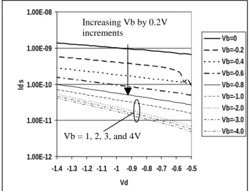
speed. Figure 2 shows that application of reverse body bias Vb is worthwhile, with nearly two orders of magnitude of leakage reduction for about 2V of reverse body bias at Vcc = 1V. Depending on the process, the Ioff may be driven below a gate leakage
value of approximately 5-8pA/µm of gate width (typical for a 0.13µm process), depending on the drain bias. This takes the total clamp leakage to a low level, so that it no longer dominates the core leakage. Simulations have shown that the circuit performs acceptably at all temperature and process corners. The low standby power is accomplished without significantly increasing the layout area since the circuitry to perform the reverse body biasing need only supply the well leakage current. A small, low current circuit to apply the body bias incidentally allows the ESD event to provide forward body bias, thereby increasing the transistor drive current when clamping.
It is well known that subthreshold leakage is typically the dominant leakage component of the minimum-length, non-back biased device [8]. But there are other contributors to the off-state leakage of a MOS device. Device scaling has encouraged process developers to reduce oxide thickness and to increase doping levels in the channel and/or in halo implants [9]. These innovations, while successful in
controlling short-channel effects, have caused significant increases in gate tunneling and junction band-to-band tunneling currents [10-11]; e.g., the gate-to-drain component of the gate oxide leakage does not decrease through backgating. And while subthreshold current decreases with increased body bias, junction leakage increases with body bias due to the higher junction voltages. Thus the influence of backgating will be limited in newer process generations as these other leakage mechanisms grow in their influence [12]. Nonetheless, the circuit in Fig. 1 significantly reduces leakage current in the 0.18µm and 0.13µm generations, especially at high temperatures and fast process corners, at which substantially higher levels of subthreshold leakage exist.
1.00E-12 1.00E-11 1.00E-10 1.00E-09 1.00E-08
-1.4 -1.3 -1.2 -1.1 -1 -0.9 -0.8 -0.7 -0.6 -0.5 Vd
Id
s
Vb=0 Vb=-0.2 Vb=-0.4 Vb=-0.6 Vb=-0.8 Vb=-1.0 Vb=-2.0 Vb=-3.0 Vb=-4.0
Figure 2. Drain to source leakage (Ioff) of PMOS transistors on a
0.18µm process at room temperature
A. Lowering leakage in a clamp for
single gate oxide through stand-alone
backgating
Sometimes a higher supply voltage will not be available for backgating the n-well as described above. In that event, some reduction of the standby leakage can still be achieved by building a small amount of backgating into the clamp design, at the expense of some area. Figure 3 shows a design that uses the same drive circuitry as described in [6,7], only it drives a double-gate FET stack for which both devices P1 and P2 are in the same n-well. Accordingly, the lower FET P2 will have its n-well approximately one threshold voltage Vtp above its source, where it is effectively back-gated. Leakage is lower than for a single gate clamp because the backgating of the series FET P2 limits the current. Additionally, the slightly positive gate to source
Increasing Vb by 0.2V increments
voltage further decreases the P2 Ioff. P1 Ioff is reduced
due to lower Vds. Informally, this design is sometimes
known as “one for the price of two”, but the actual area increase is only about 50% because of the efficiency of layout of a double gate. Table 1 (see section IV) shows how, in a 0.18µm process, the leakage of this kind of clamp (pmoslwlk, Figure 3) is cut to about 30% of the leakage of a standard PMOS clamp device (pmos1, designed as in [6,7]).
Vss
P1
Vcc
P2
Vcc
Figure 3. Low- leakage PMOS clamp with double gate on large device and built-in back bias for P2
III. Lowering leakage in
stacked-gate clamps for higher voltages
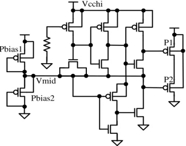
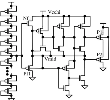
Contemporary product designs often have multiple voltage supplies. When the voltage exceeds the allowed voltage for a single thin gate oxide, we need new methods for protecting the supply itself. For low power products we must improve on the 2-stack and multi-stack clamps in [13-16], which commonly require at least 0.5 to 1µA of standby current. These stacked clamps have their midpoint Vmid biased by resistive long-channel devices Pbias1 and Pbias2 as in Figure 4 [15]. The following methods are aimed at stacked-gate clamps for high voltages, using bias circuits with much lower standby current.Figure 5 shows an example of a two-stack voltage tolerant clamp with low bias current. Rather than use a resistive voltage divider to establish the midpoint voltage Vmid between Vcc and Vss, we now use a long string of slightly-on subthreshold devices to establish the midpoint voltage. These devices need only drive the small gates of two follower FETs Pf1 and Nf1 in Fig. 5. Pf1 and Nf1 in Fig. 5 are a voltage buffer that turns the weak voltage Vref into a fairly strong voltage source for Vmid, such that Vref-Vtp<Vmid<Vref+Vtn. The buffer Pf1 and Nf1 then sources or sinks just enough current to supply the subthreshold currents of the bias circuitry, a fairly
small requirement. In practice, it is Nf1 that nearly always turns on to supply extra current to the lower half of the circuit, since its NMOS FETs have no substrate back bias. The subthreshold current of the wide PMOS clamp FETs P1 and P2 then dominates the standby leakage of the entire circuit; as shown in Table 1 the improvement is over 50%. The remainder of the bias circuitry in Fig. 5 for the stacked clamp is exactly as in [13-16]. The devices in the subthreshold string are small in size (0.4/2) so that a long string will not use much area or consume much current. The transistors are tied identically, providing good consistency across process corners. The area impact of the extra bias circuitry required for these designs can be held to less than 10% (and one must carefully optimize the layout of both designs to see any impact at all). This method of supplying bias for low leakage stacked clamps can be generalized to stacks of three or more clamping devices and bias circuits, thus raising the voltage that can be clamped.
Vcchi
Pbias1
Vmid
P1
P2
Pbias2
Figure 4. Standard stacked PMOS clamp with resistive bias through Pbias1 and Pbias2, fixing midpoint Vmid at about half of Vcchi
IV. Leakage Results
P1 Vcchi
P2 Vmid
Pf1 Nf1
Figure 5. 2-stack voltage-tolerant clamp with reduced bias current
Table 1. Thin gate oxide clamp designs compared for leakage on a 0.18µm process
PMOS Clamp design, 0.18µµµµm
Leakage, 27C (µµµµA)
Leakage, 110C (µµµµA)
pmos1, regular clamp cell 0.413 11 back-gated pmos1, Fig. 1 0.064 3.52
pmoslwlk, Fig. 3 0.132 2.83 2-stack cell, Fig. 4, from
[13-15]
0.650 17.3
2-stack low-leak clamp, Fig. 5
0.300 8.65
Now we turn to the same kind of designs on the 0.13µm process [19]. This process introduced substantial gate leakage and had an effect on total leakage as well as the circuits used in ESD power supply clamps [15-16]. As shown in Table 2, leakage was always in the microamp range, and moving to the new circuits such as in Figs. 3 and 5 was not very effective. There was some effect at high temperature with backgating as in Figs. 1 and 3. As expected, backgating was most effective at reducing leakage for the low-VT end of the process and at high
temperature. As discussed earlier, increased gate oxide and junction leakage puts some limits on the effectiveness of backgating at this process node. Fortunately, the products intended for low leakage applications in the 0.13µm process are typically
implemented in a process version supporting two oxide thicknesses, so there is also a far less leaky thick gate oxide, tolerant of 2.5V and intended for I/O, which can be used for power supply clamps.
Table 2. Thin gate oxide clamp designs compared for leakage on a 0.13µm process. Typical results are shown; at the low-VT or “fast” end of the process, there is more
leakage and more effect due to backgating
PMOS Clamp design, 0.13µµµµm Leakage, 25C (µµµµA)
Leakage, 125C
(µµµµA)
latched regular clamp cell, [15] 6.8 22.9 back-gated pmos1, Fig. 1* 6.7 11.7 pmoslwlk, Fig. 3* 6.7 12.3 2-stack cell, Fig. 4, from [13-15]* 5.1 19.0 2-stack low-leak clamp, Fig. 5* 5.7 20.6
*with latch circuit as in [15]
Table 3 shows the typical leakage results for ESD power clamps made with thick gate oxide devices in the 0.13µm process. Using a familiar design for non-leaky gate oxides [7], essentially Fig. 1 without the backgating, standby leakage is fairly low. Adding backgating to this design as in Fig. 1 does not reduce the low-temperature leakage by much, but does reduce high-temperature leakage to about one microamp at typical and fast (i.e., typical and low VT)
process corners.
Table 3. Thick gate oxide clamp leakage results on a 0.13µm process
PMOS Clamp design, 0.13µµµµm Leakage, 25C (µµµµA)
Leakage, 125C (µµµµA)
regular thick gate clamp cell, [7], 2.5V
0.63 10.2
thick gate clamp cell, [7], 1.3V 0.19 5.9 2-stack cell, Fig. 4, 3.3V,
from [13-15]
1.7 9.8
2-stack low-leak clamp, 3.3V, Fig. 5
0.35 9.5
2-stack cell, Fig. 4, 5V, from [13-15]
4.0 17.1
2-stack low-leak clamp, 5V, Fig. 5
Table 3 also shows that using the low-leakage circuits as in Fig. 5 provides substantial improvement in standby leakage at lower temperatures, over Fig. 4 for the 2-stack thick oxide clamp in the 0.13µm process. But it is at these lower temperatures where the low standby current is most desired, when the component is idling. Since the high temperature leakage is mostly temperature-dependent subthreshold leakage in the main clamping FETs, backgating would be available for reducing that leakage if it were desired.
V. Discussion and Conclusions
The theme of this work is to arrive at ESD power clamp designs which will have the same performance as traditional clamp designs [6-7,13-16] yet will have lower standby leakage current. All the designs discussed herein have virtually the same Human Body Model (HBM), Charged Device Model (CDM), and transmission line pulse (TLP) results as discussed in those earlier references. The intention is for HBM and CDM to be high enough (e.g., over 4kV HBM and over 1kV CDM on the KeyTek Zapmaster) to prove self-protection of the clamps, and enough pulsed TLP current at low voltage (e.g., 2A at about 4V as in [15]) to protect other circuitry on the power supply. In short, the ESD performance impact of the low-leakage circuitry discussed herein was negligible. This is because the ESD current is sunk through the large FETs, which are unchanged. We made sure the gate drive and timing would be unaffected by the low leakage circuitry, through circuit simulation.In recent times there has been renewed interest in the power-up transient associated with these RC-timed clamps. The fastest anticipated ramp times (slew rates) are getting faster, and there is more frequent dynamic power-up and power-down of circuits. The increase in battery-powered applications motivates us to look at total charge consumption on power-up, and to put bounds on how weak a power supply (i.e., how high an output impedance) might have to power up these clamps. The good news about the low-leakage circuits in this paper is that there was little if any impact on the basic behavior of the ESD clamps’ power-up transient. Again, the reason is that the clamp FETs are unchanged, and the gate drive timing of those FETs is also largely unchanged.
As we investigate power-up transients in the light of broader applications, it is useful to reflect on a basic fact brought out in our early work on the subject of ESD power clamps [20,21], the fact that the total amount of charge needed to power up these clamps is a few microcoulombs. This makes sense based on amps of current for RC-timed microseconds, of
course. The fast (nanosecond scale) ramp requires the most charge, and the required charge declines from there, with a 100µs power ramp’s charge pulse down by a factor of ten to a few hundred nanocoulombs. But note how these quantities of charge compare with battery charges, which are measured on the scale of ampere-hours. 3.6µC is a billionth of an ampere-hour! This illustrates a fundamental principle of electrostatic phenomena that we should all know, which is that the currents and voltages in ESD can be high, but the amount of charge is small.
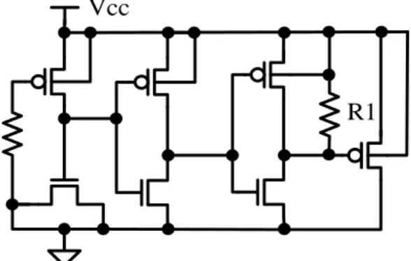
If total charge for power-up is of any concern, it can still be reduced for the longer times common to power-up of the supply by a voltage source. Table 4 shows the charge quantities associated with ramp times from fast to slow, and how they are influenced by adding a simple pullup resistor of a few hundred ohms, R1, as in Figure 6. For ramp times of 100µs and above, note that total charge required drops by over two orders of magnitude. The transient for an ESD-like fast ramp, and the total charge pulse, is not affected.
Table 4. Charge quantities, in microcoulombs, for power-up of a simple ESD clamp using 2.5V gate oxide, designed as in Fig. 6, with and without pullup resistor R1
Voltage ramp time
Charge, no pullup (µµµµC)
Charge, with pullup (µµµµC)
1 nsec 3.54 3.56
10µsec 2.96 2.84 100µsec 0.43 0.002
1 msec 0.089 0.00028
In addition, the R1 in Fig. 6 adds a threshold-free device between clamp FET gate and source, and largely removes any concern about VT effects on the
relieved those concerns without compromising ESD performance.
Vcc
R1
Figure 6. Regular PMOS single oxide clamp with pullup resistor R1 (several hundred ohms) that reduces the power-up transient for ramp rates slower than ESD
In conclusion, we have presented circuits for reducing leakage in a variety of MOS ESD power supply clamps in 0.18µm and 0.13µm processes. The circuits have enabled substantial reduction of leakage without compromising ESD performance. A large payoff in leakage reduction comes with various backgating schemes to reduce the subthreshold leakage of the clamping MOSFETs (PMOS in our case, but the same principles would apply to NMOS). These effects are most pronounced when that subthreshold leakage dominates the total leakage, and are less noticeable when gate oxide leakage is substantial. In addition, stacked voltage-tolerant ESD clamps benefit from improving on the resistive voltage divider as a way to establish internal bias in the clamp. An active circuit targets the bias current distribution in a more efficient way and reduces leakage current in these clamps for all processes, whether or not gate oxide leakage is substantial. Finally, the total charge required for power-up of the supply clamp at ordinary supply ramp rates can be reduced by adding a single resistive element to the circuit, but this has no appreciable effect on the circuit’s behavior at the ESD time scale.
Acknowledgements
The authors wish to thank Tina Cantarero for many of the lab measurements, and Pradeep Elamanchili who contributed to some of the circuits reported in this work. We also thank Mohsen Alavi, Babak Sabi and Jay Heeb for managerial support.
References
[1] S. Mutoh, et al., “1-V Power Supply High-Speed Digital Circuit Technology with
Multithreshold-Voltage CMOS,” IEEE J. of Solid-State Circuits, 30, pp. 847-854 (1995).
[2] H. Mizuno, et al., “An 18-µA Standby Current 1.8V, 200MHz Microprocessor with Self-Substrate-Biased Data-Retention Mode,” IEEE J. Solid-State Circuits, 34, pp. 1492-1500 (1999). [3] L. T. Clark, et al., “Standby Power Management
for a 0.18µm Microprocessor,” Proc. 2002 International Symposium on Low Power Electronics and Design, pp. 7-12.
[4] L. T. Clark, “A High-Voltage Output Buffer Fabricated on a 2V CMOS Technology,” Proc. 1999 IEEE Symposium on VLSI Circuits, pp. 61-62.
[5] G. B. Singh and R. B. Salem, “High-Voltage-Tolerant I/O Buffers with Low-Voltage CMOS Process,” IEEE J. of Solid-State Circuits, 34, pp. 1512-1525 (1999).
[6] T.J. Maloney and T.M. Eiles, US Patent 5,907,464; issued May 25, 1999, assigned to Intel Corp.
[7] T.J. Maloney, "Designing Power Supply Clamps for Electrostatic Discharge Protection of Integrated Circuits", Microelectronics Reliability 38, No. 11, pp. 1691-1703 (November, 1998).
[8] B. Doyle et al., "Transistor Elements for 30nm Physical Gate Lengths and Beyond." Intel Technology Journal. http://developer.intel.com/ technology/itj/2002/volume06issue02/ (May 2002).
[9] R. Chau et al., "30 nm physical gate length CMOS transistors with 1.0 ps n-MOS and 1.7 ps p-MOS gate delays," IEDM Tech. Digest, 2000, pp. 45-48.
[10] T. Ghani et al., "Scaling challenges and device design requirements for high-performance sub-50 nm gate length planar CMOS transistors," VLSI Symposium Tech. Digest, 2000, pp. 174-175.
[11] B. Yu et al., “50nm Gate-Length CMOS Transistor with Super-Halo: Design, Process, and Reliability,” IEDM Tech. Digest, 1999, pp.653-655.
[13] T.J. Maloney, US Patent 5,956,219, issued Sept. 21, 1999, assigned to Intel.
[14] T.J. Maloney and W. Kan, "Stacked PMOS Clamps for High Voltage Power Supply Protection", 1999 EOS/ESD Symposium Proceedings, pp. 70-77. Also published in Microelectronics Reliability 41, No. 3, pp. 335-348 (March, 2001).
[15] S.S. Poon and T.J. Maloney, "New Considerations for MOSFET Power Clamps", 2002 EOS/ESD Symposium Proceedings, pp. 1-5.
[16] T.J. Maloney and W. Kan, "RC Timer Scheme", US Patent 6,510,033, issued Jan. 21, 2003, assigned to Intel.
[17] L.T. Clark, P. Elamanchili, T. Maloney, "Electrostatic Discharge Protection Device and Method Therefor", US Patent application, filed Dec. 22, 2000.
[18] L.T. Clark, et al., “An Embedded 32-b Microprocessor Core for Low-Power and High-Performance Applications”, IEEE J. Solid-State Circuits, 36, pp. 1599-1608 (2001).
[19] S. Tyagi et al., “A 130 nm Generation Logic Technology Featuring 70 nm Transistors, Dual Vt Transistors and 6 Layers of Cu Interconnects”, IEDM Tech. Digest, 2000, pp. 567-570.
[20] T.J. Maloney and S. Dabral, "Novel Clamp Circuits for IC Power Supply Protection", 1995 EOS/ESD Symposium Proceedings, pp. 1-12. Revised version published in IEEE Trans. on Components, Packaging, and Manufacturing Technology--Part C, 19, 150-161, July 1996.
[21] S. Dabral and T.J. Maloney, Basic ESD and I/O
Design, published by Wiley Interscience,
November 1998, 302 pages.