QUICK START GUIDE FOR DEMONSTRATION CIRCUIT 908A
POLYPHASE 3-OUTPUT STEP-DOWN SUPPLY WITH TRACKING
LTC3773EG
DESCRIPTION
Demonstration circuit 908A is a Polyphase 3-Output Step-Down Supply with Tracking featuring the LTC3773EG. The output voltages are 3.3V, 2.5V and 1.8V and the maximum load current for each is 15A. The input voltage range is 7V to 24V. Typical applications include servers, communica-tions, computers and industrial power supplies.
The board can be programmed for either continu-ous-conduction mode (CCM), pulse skip mode (DCM) or Burst Mode (BM). Other features of the
board include an SDB pin which can be used for rail sequencing, a phase mode pin, and a dynamic load circuit for each rail.
An on-board LT1933 (5V / 500mA buck converter) provides current for the LTC3773EG’s internal logic and gate drive circuitry. The 5V bias can also be supplied externally. If an external bias voltage is applied it needs to be between 4.5V and 7.0V.
Design files for this circuit board are available. Call the LTC factory.
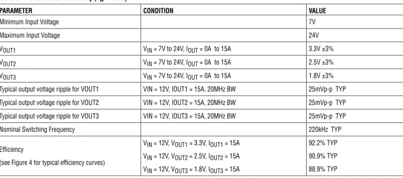
Table 1. Performance Summary (TA = 25°C)
PARAMETER CONDITION VALUE
Minimum Input Voltage 7V
Maximum Input Voltage 24V
VOUT1 VIN = 7V to 24V, IOUT = 0A to 15A 3.3V ±3%
VOUT2 VIN = 7V to 24V, IOUT = 0A to 15A 2.5V ±3%
VOUT3 VIN = 7V to 24V, IOUT = 0A to 15A 1.8V ±3%
Typical output voltage ripple for VOUT1 VIN = 12V, IOUT1 = 15A, 20MHz BW 25mVp-p TYP Typical output voltage ripple for VOUT2 VIN = 12V, IOUT2 = 15A, 20MHz BW 25mVp-p TYP Typical output voltage ripple for VOUT3 VIN = 12V, IOUT3 = 15A, 20MHz BW 25mVp-p TYP
Nominal Switching Frequency 220kHz TYP
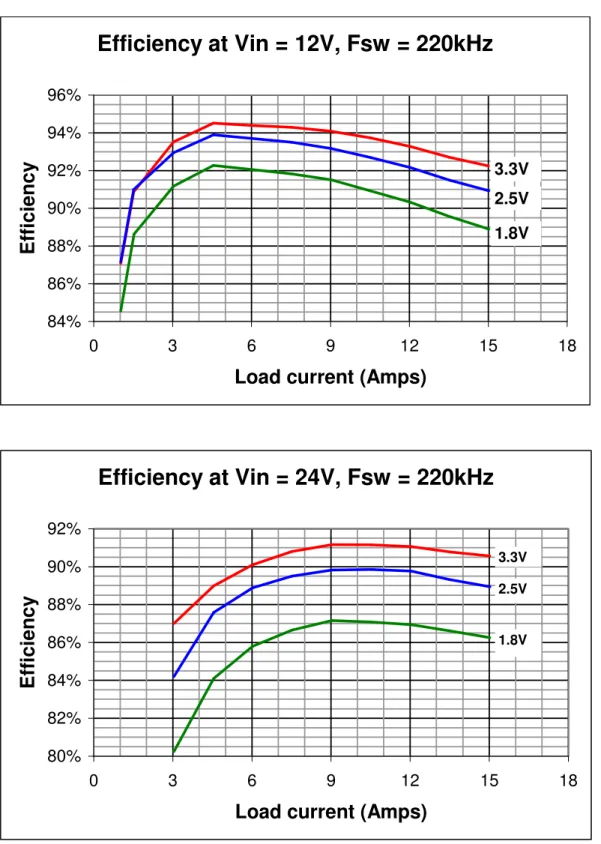
Efficiency
(see Figure 4 for typical efficiency curves)
VIN = 12V, VOUT1 = 3.3V, IOUT1 = 15A VIN = 12V, VOUT2 = 2.5V, IOUT2 = 15A VIN = 12V, VOUT3 = 1.8V, IOUT3 = 15A
92.2% TYP 90.9% TYP 88.9% TYP
QUICK START GUIDE FOR DEMONSTRATION CIRCUIT 908A
POLYPHASE 3-OUTPUT STEP-DOWN SUPPLY WITH TRACKING
QUICK START PROCEDURE
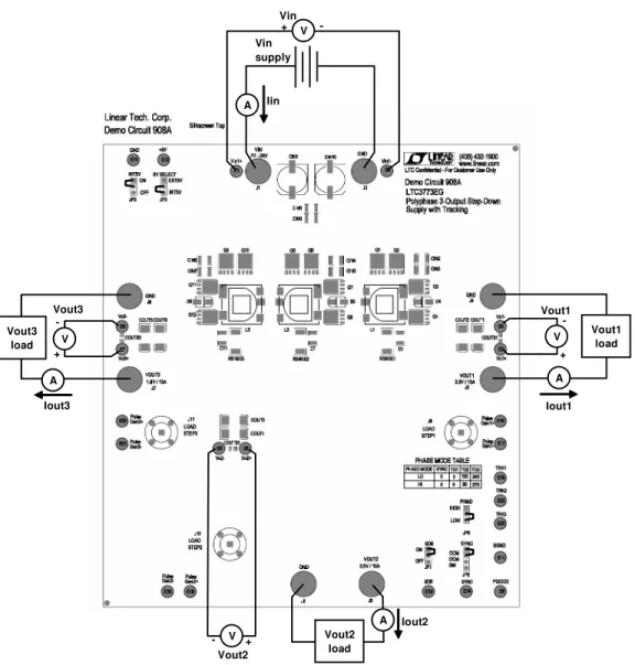
Demonstration circuit 908A is easy to set up to evaluate the performance of the LTC3773EG. Refer to Figure 1 for proper measurement equipment setup and follow the procedure below:
NOTE: When measuring the output voltage ripple, care must be taken to avoid a long ground lead on the oscil-loscope probe. Measure the output voltage ripple by touching the probe tip directly across the Vout and GND terminals. See Figure 2 for proper scope probe tech-nique.
1. Place the jumpers as shown below:
Description JP# Position INT5V JP5 ON 5V SELECT JP3 INT5V SDB JP1 ON SYNC JP2 CCM PHMD JP6 LOW
2. With power off, connect the input power supply to Vin and GND.
3. Turn on the input voltage and set it to a voltage be-tween 7V and 24V. The input voltage source should be able to supply at least 20A.
NOTE: Make sure the input voltage does not exceed 24V.
4. Check for the proper output voltages: Vout1 = 3.201V to 3.399V
Vout2 = 2.425V to 2.575V Vout3 = 1.746V to 1.854V
5. Once the proper output voltages are established, adjust the loads within the operating range and ob-serve the output voltage regulation, ripple voltage, efficiency and other parameters.
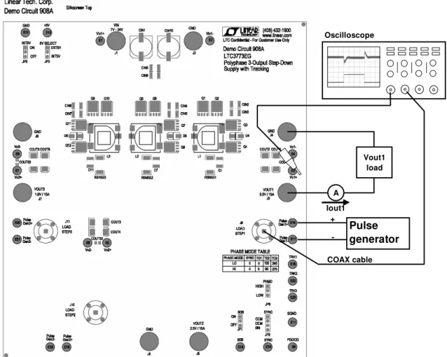
LOAD STEP RESPONSE
The load step response for each rail can be tested with an on-board dynamic load circuit and a pulse generator. Refer to Figure 3 and follow the steps below.
1. Set the output of the pulse generator for a duty cycle of less than 5% and an amplitude of 1V or below. 2. Connect the output of pulse generator from Pulse
Gen+ to Pulse Gen-.
3. Connect the LOAD STEP BNC connector to an
oscil-4. Turn-on the 908A and apply the desired amount of static load to the output.
5. Increase the amplitude of the pulse generator output to obtain the desired load step height.
6. Monitor the output voltage across the turrets as shown.
QUICK START GUIDE FOR DEMONSTRATION CIRCUIT 908A
POLYPHASE 3-OUTPUT STEP-DOWN SUPPLY WITH TRACKING
RAIL TRACKING AND SEQUENCING
The DC908A is setup for coincident rail tracking, where both Vout2 and Vout3 track Vout1 directly through their TRACK pins and TRACK dividers. Refer to Figure 5 for the turn-on waveforms. The ramp-rate for Vout1 is de-termined by a 10nF capacitor on the TRACK1 pin at C8 on the demo board. If desired, Vout1 can be setup to track an external signal. To do this, remove C8 and stuff the appropriate values for the TRACK 1 divider at R40 and R41 and apply the tracking signal to the TRACK1 turret.
If desired, the rails can be configured to be turned on and off independently. To do this, remove the TRACK2 and TRACK3 dividers at R33, R35, R38 and R39, and stuff TRACK capacitors at C31 and C32 to set the de-sired ramp-rate. Rail sequencing can be implemented by placing a capacitor on the SDB pin. As the voltage on the SDB pin ramps-up, Vout1 will turn on 1st
, Vout2 will turn on 2nd
and Vout3 will turn-on last. Refer to the data sheet for more details on rail tracking and sequencing.
V A + -Vin Iin Vin supply Vout1 load A Iout1 + -V -Vout1 Vout2 load A Iout2 + V -Vout2 Vout3 load A Iout3 + V -Vout3
QUICK START GUIDE FOR DEMONSTRATION CIRCUIT 908A
POLYPHASE 3-OUTPUT STEP-DOWN SUPPLY WITH TRACKING
V
O
U
T
G
N
D
Figure 2. Measuring Output Voltage Ripple
+ -Oscilloscope Vout1 load A Iout1 Pulse generator COAX cable
QUICK START GUIDE FOR DEMONSTRATION CIRCUIT 908A
POLYPHASE 3-OUTPUT STEP-DOWN SUPPLY WITH TRACKING
Efficiency at Vin = 12V, Fsw = 220kHz
84% 86% 88% 90% 92% 94% 96% 0 3 6 9 12 15 18Load current (Amps)
E
ff
ic
ie
nc
y
3.3V 1.8V 2.5VEfficiency at Vin = 24V, Fsw = 220kHz
80% 82% 84% 86% 88% 90% 92% 0 3 6 9 12 15 18Load current (Amps)
E
ff
ic
ie
nc
y
3.3V 1.8V 2.5VQUICK START GUIDE FOR DEMONSTRATION CIRCUIT 908A
POLYPHASE 3-OUTPUT STEP-DOWN SUPPLY WITH TRACKING
3.3V 2.5V 1.8V SDB 2V / div 2msec / div Vo1,2,3 1V / div