Patching Circuit Design Based on Reserved CLBs
A. Matrosova, S. Ostanin,V. Andreeva Department of Applied Mathematics and Cybernetics
Tomsk State University (TSU) Tomsk, Russia
[email protected], [email protected], [email protected] Abstract—The new approach to patching circuit design
that allows masking any logical gate faults of combinational circuit (combinational part of sequential circuit) C is considered. It is supposed that only one gate may be fault. There are reserved Configurable Logic Blocks (CLBs) based on Look Up Tables (LUTs) that may mask a gate fault being included into the circuit through Multiplexer (MUX). The suggested approach to patching circuit design in contrast with currently in use allows keeping performance of a fault free circuit. It is suggested to include MUXs in those internal poles of circuit C that may have hard detectable faults. Experimental results showed that masking LUT based circuits are as a rule, rather simple.
Keywords—stuck-at faults, arbitrary faults, test patterns, incompletely specified Boolean functions, patching circuit design.
I. INTRODUCTION
The growing size, density and complexity of modern VLSI chips are contributing to increase hardware faults and design errors in the silicon, decreasing the manufacturing yield and increasing the design cycle [1]. There has been investigated several practical techniques to increase the yield of VLSIs [2-4]. A general technique is to add space redundancy, e.g., Triple Modular Redundancy (TMR). If we are considering only manufacturing defects, another possible way to increase the yield is Double Modular Redundancy (DMR). In this case we select a module without a defect between identical modules after the VLSI test. Embedded FPGAs have also been used for yield improvement [5-6]. However, the above methods have disadvantages: area overhead and/or performance degradation. In [7, 8] the different approaches to increase the yield with lower overhead have been proposed. There has been used a circuit obtained from a conventional logic circuit from gates by replacing its sub-circuits with Look-Up Tables (LUTs) and Multiplexers (MUXs). Then, if we detect some defects (by the VLSI test), we reconfigure the functionality of some LUTs and MUXs to bypass the defects (single stuck-at faults). This kind of circuits is called Partially Programmable Circuits (PPCs) since some of their parts are programmable. The approach is based on the representation of the sub-circuit behavior of a combinational circuit by the incompletely specified Boolean function. In [9] SAT-based rectification and debugging method based on using PPCs for combinational circuits with LUTs is presented. In [10] a patchable
hardware architecture where functional modifications are achieved by introducing memory elements in a circuit is proposed.
In [11] the method using compact (with two Reduced Ordered Binary Decision Diagrams – ROBDDs) implementation of an incompletely specified Boolean function to mask any gate fault for one output combinational circuit is suggested. It applies a multiplexer in each combinational circuit branch. When the fault of a gate is detected, the proper replacing sub-circuit from reserved Configurable Logic Blocks (CLBs) is constructed. Its output is connected with the circuit through the closest multiplexer in the branch point. The sub-circuit masks either the arbitrary fault of the gate which output is the branch point or the arbitrary fault of any gate for which this branch-point is the closest one but its own output is not a branch point.
In this paper the above mentioned method [11] was spread to multi output combinational circuits (combinational parts of sequential circuits). The strategy of choosing internal poles for including multiplexors is suggested. Unlike the approaches [7-9] our approach allows keeping performance of a fault free circuit.
In Section II implementations of the incompletely specified Boolean function for single and multi output circuits are considered. In Section III the ways of masking faults are discussed. The experimental results are presented in Section IV.
II. IMPLEMENTATION OF THE INCOMPLETELY SPECIFIED BOOLEAN FUNCTION FOR SINGLE AND MULTI OUTPUT
CIRCUITS
Let v be a selected internal node of a combinational single output circuit C consisting of gates. The problem of a selection of poles we will discuss later. Correlate v to a multiplexor (MUX). Pole v (output of a fault free gate) is connected with one MUX input. If the gate with output pole v is fault then the output of the special masking sub-circuit is connected with another MUX input. The sub-circuit consisting of CLBs masks any logical fault of the gate. Describe a derivation of a masking sub-circuit. Note that the sub-circuit is implementation of incompletely specified Boolean function corresponding to pole v. Let f be the completely specified Boolean function that is implemented by the fault free sub-circuit with the output pole v and inputs coinciding with inputs of circuit C. Correlate stuck-at
fault 0 (ı = 0) and stuck-at fault 1 (ı = 1) to pole v. We use these faults to represent the incompletely specified Boolean function describing behavior of the sub-circuit being included in circuit C. The real fault of the gate with output pole v may be arbitrary. In [12, 13] the method of finding all test patterns for fault ı = 0 (ı = 1) and presenting them by the ROBDD is suggested. It is based on results obtained in [14].
Let fv0 be the function that represents all test patterns
for fault ı = 0 at pole v. Let fv1 be the function that
represents all test patterns for fault ı = 1 at pole v. Let ij (X) be the function implemented by circuit C and Ȣ (X, v), X = {x1,…, xn}, be the function implemented by the sub-circuits of circuit C in which pole v is considered as the input variable along with a set X and the output coincides with circuit C output: Ȣ (X, f) = ij (X). We conclude that any test pattern for the fault ı = 0 (ı = 1) at pole v turns function f ( f ) into 1 and turns function ij (X) either into 1 or into 0. Moreover changing the value at pole v from 1 to 0 (from 0 to 1) for fault ı = 0 (ı = 1) generates changing the value at circuit C outputfrom 1 to 0 if the test pattern turns fault free circuit C output into 1 and from 0 to 1 if the test pattern turns fault free circuit C output into 0.
Note that if a Boolean vector of length n turns function f into 0 (into 1), then it cannot be a test pattern for fault ı = 0 (ı = 1) at pole v.
They say f includes g (g is an implicant of f), g f, if for any Boolean vector Į of length n from the condition g(Į) = 1 follows the condition f(Į) = 1. For fault ı = 0 we have: f f,v0 for fault ı = 1: f v1 f .
Let the condition fv0≤ε≤ fv1 for the function İ takes
place.
Theorem 1. Ȣ(X, f) = Ȣ(X, İ), that is changing the
function f for the function İ does not alter function ij (X). Let the function Ȗ be as follows: fv1≤γ≤ fv0.
Theorem 2. Ȣ(X, f) = Ȣ(X, γ), that is changing the
function f for the function γ does not alter the function ij(X).
Explain Theorems 1, 2 using the Venn diagrams in Fig. 1.
Fig. 1. Representation of the incompletely specified Boolean function for pole v
All spots of the rectangle represent all Boolean vectors of length n. These spots are divided into on-set 1
f
M and
off-set 0
f
M of completely specified function f by wavy line. The oval inside of 1
f
M area presents the on-set of function 0
v
f corresponding to a set of all test patterns for fault ı = 0 at pole v of circuit ɋ. The oval inside of 1
f
M area presents the on-set of function fv1corresponding to a set of all test patterns for fault ı = 1 at pole v of circuit ɋ. The dashed part of the rectangle is don’t care area of the incompletely specified Boolean function. The on-set and the off-set of this function are represented with the on sets of functions fv0 , fv1 , correspondingly. Taking into
consideration Theorems 1, 2, when masking fault, we may choose the circuit that implements either function İ, or functionγ. Both these functions may be represented with the corresponding ROBDDs. The chosen ROBDD may be covered with CLBs (to get the circuit whose behavior is represented by this ROBDD) in the way described in [15].
Proposition 1. The behavior of any sub-circuit of single output combinational circuit C is described with incompletely specified Boolean function finc. The on-set of
finc is represented by the on-set of function f and the off- v0 set of finc is represented by the on-set of functionf . v1
This proposition takes place for any internal pole of a single output circuit C. For finding a minimum masking circuit realization we can use one of the heuristic algorithm ROBDD minimization for incompletely specified Boolean functions, for instance [16]. Let f*(X) be the completely specified function that realizes the incompletely specified function (presented by f v0 and fv1) and has minimized
ROBDD size. Use ROBDD of function f* to mask the fault of the gate with output pole v.
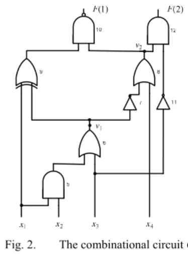
The example of two output circuit C is given in Fig. 2. Consider the one output sub-circuit of circuit C corresponding to output F(1).
Fig. 2. The combinational circuit ɋ
Extract functions fv0(1), fv1(1), f (1), f*(1) for pole v1.
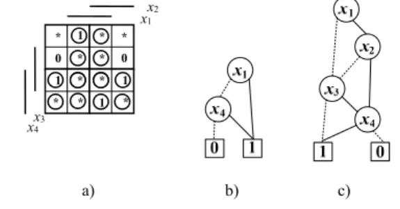
Represent incompletely specified function with K-map in Fig. 3a. Here the on-set is represented with 1s, the off-set is represented with 0s and don’t care set is represented with asterisks. Mark elements of the on-set for function f*(1) by 0 v f 1 v f 1 f M 0 f M
circles. For pole v1 function f*(1) coincides with f(1). The
ROBDD of f(1) has minimized number of nodes (Fig. 3b).
a) b)
Fig. 3. a) K-maps of the functions for pole v1; b) ROBDD for f* = f Extract functions fv0(1), fv1(1), f (1), f*(1) for pole v2.
Represent the incompletely specified function with K-map in Fig. 4a. In this case the size of the ROBDD for function f*(1) is less in comparison with the ROBDD for f(1) (Fig. 4b-c).
a) b) c)
Fig. 4. a) K-maps of the functions for pole v2; b)ROBDD for f*(1); c)
ROBDD for f(1)
Consider a multi output circuit C. If all paths of internal pole v are connected with the same output we have the situation has already been considered.
Let the paths of pole v be connected with the different outputs of circuit C: i1,…, is. In this case we may obtain two
ROBDDs for each incompletely specified Boolean function finc(ij) corresponding to ij output of circuit C, ij∈{i1,…, is}. Its on-set is represented by the on-set of function fv0(ij) and the off-set is represented by the on-set of function
1
v
f (ij). These on-sets are represented by the proper ROBDDs derived from the single output sub-circuit with ij output and considered pole v in above mentioned way.
Then we form ROBDD ( fv0) having executed the
disjunction operation over ROBDDs representing functions 0
v
f (i1),…, fv0(is) and ROBDD (fv1 ) having executed the
disjunction operation over ROBDDs representing functions 1
v
f (i1),…, fv1(is). At last, wederive ROBDD representing
function f* for pole v. The obtained ROBDD we may use for masking arbitrary fault of the gate with output pole v.
Illustrate this algorithm on two output circuit C from Fig. 2. Extract functions fv0 (2), fv1 (2) for pole v2
(functions fv0(1), fv1(1) has already been extracted above).
Represent incompletely specified function for pole v2 and
output F(2) with K-map in Fig. 5a. Fig.5b shows incompletely specified function for pole v2 common for all
outputs of the circuit C, fv1= fv1(1)∨ fv1(2) (on-set),
0
v
f = fv0(1)∨ fv0(2) (off-set).
a) b)
Fig. 5. a) K-map of the incompletely specified function for pole v2
and output F(2); b) K-map of the incompletely specified function common for all outputs which is presented by fv1 and fv0 In Fig. 6a K-map for function f*is shown. For pole v2
common for all outputs function f* coincides with f. The ROBDD of f* has minimized number of nodes (Fig. 6b).
a) b)
Fig. 6. a) K-map for f*; b) ROBDD for f*
In the end of this section consider some special cases for additional optimization.
Let one of the functions fv1 or fv0 be equal to 0. The
function fv1 = 0. This situation is represented by the Venn
diagram of Fig. 7a. This means that the function İ may be changed for the constant 1. As a result we may mask the considered gate fault by a connection of the proper MUX input with a power source.
The function fv0 = 0. This situation is represented by
the Venn diagram of Fig. 7b. This means that the function Ȗ may be changed for the constant 1. As a result we may mask the considered gate fault by a connection of the corresponding MUX input with a ground.
If fv1 = 0 and fv0 = 0 we have: Ȣ(X, 1) = Ȣ(X, 0) that is
the variable v is unessential. In this case the fault gate does not change the function ij(X). There is no need to mask such fault.
a) b)
Fig. 7. Representation of the incompletely specified Boolean function for pole v: a) fv1 = 0; b) fv0 = 0 1 v f 1 f M 0 f M 0 v f 1 f M 0 f M x1 x2 x3 x4 0 1 1 0 1 1 1 1 1 1 1 1 1 0 1 1 x1 x2 x3 x4 0 * * 0 1 * * 1 1 1 1 1 1 0 1 1 x1 x2 x3 x4 0 * * * * * * * 1 1 1 1 1 * 1 1 x1 x2 x3 x4 * * * 0 1 * * 1 1 * * * * 0 1 * x1 x2 x3 x4 1 * 1 1 * 1 1 1 1 1 0 0 * * 0 0 *
III. MASKINGFAULTS
ROBDD presentation of function f* derived either for single or multi output combinational circuit C is covered by LUT based CLBs. In partly, covering one internal pole v of ROBDD we need one output LUT with three inputs.
Consider sub-circuit Cv** of circuit C with output v. The sub-circuit inputs are either the closest to v branch points of circuit C or circuit C inputs. Let a fault gate with the output pole w belong to the sub-circuit and be not its branch-point. We also admit any logical fault of the gate with output pole w. Change the sub-circuit implementing function f corresponding to the pole v for the proper masking sub-circuit implementing function f* in above mentioned way. As the sub-circuit with output pole w is a part of the sub-circuit with output pole v implementing function f, the fault gate with output pole w is also be masked. Note that there are no branch-points between poles v and w. This means that any fault of the gate with output pole w does not affect any gates beyond the path connecting v and w.
Thus masking the fault of the gate with output pole v we mask the fault of the gate with output pole w at the same time.
We suggest choosing internal poles v1,…, vr in circuit C so that their incompletely specified Boolean functions are weakly determined. Let the percentage of don’t care values of the functions be not less threshold h. This means that faults of gates with outputs v1,…, vr are considered as hard detectable.
Note that each selected pole originates the sub-circuit **
v
C . If any of outputs v1,…, vr is the output of the gate of other sub-circuit of this kind, we exclude this pole from a consideration to cut the number of MUXs. As a result we get more short set of internal poles and call it v1,…, vt.
Proposition 2. Any hard detectable fault of gate of circuit C may be masked with using the chosen set of poles v1,…,vt.
Thus if a fault gate in circuit C is found, a developer deɫides either this fault may be masked by the CLB sub-circuit or sub-circuit C must be redesigned. The decision depends on a complexity of the masking sub-circuit and its other characteristics.
We may consider several combinational (sequential) circuits and the proper array of reserved CLBs. For each circuit (combinational part of sequential circuit) C we find a set of internal nodes to include MUXs. Input poles of each circuit C are correlated with primary inputs (primary outputs) poles of CLBs array so that these poles of different circuits don’t intersect. We may estimate maximal complexity of masking sub-circuit for each circuit C and total number of primary input (primary output) poles to choose the proper CLBs array.
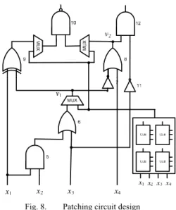
The idea of this approach is represented in Fig. 8.
Fig. 8. Patching circuit design IV. EXPERIMENTAL RESULTS
We have used MCNC Benchmark circuits for experiments. The experimental results are shown in Table 1. Here is N_in – a number of inputs; N_out – a number of outputs; Avg_ratio – an average characteristic of the incompleteness among of all functions corresponding to internal lines of the circuit, this value characterizes a possibility of a circuit simplification; H – some threshold; Pole – name of internal pole; Ratio – characteristic of the incompleteness of function corresponding to the chosen internal pole of the circuit; ROBDD_f* – the size (the number of tree inputs LUTs) of the ROBDD for f*, f* is the one of the best implementation of the incompletely specified Boolean function, the ROBDD for f* was produced by using function Cudd_bddMinimize from CUDD package. A threshold choice in each case is individual. If ratio of incompleteness for pole v is higher than the threshold we consider the fault on pole v as hard detectable. Experimental results showed that ROBDDs representing function f* for poles with don’t care values not less the given threshold are rather simple.
V. CONCLUSION
The original approach to masking arbitrary gate faults of combinational circuits based on inserting fault free sub-circuit through MUX in the proper points of the given combinational circuits (combinational part of sequential circuit) C is developed. The sub-circuit is derived by covering the corresponding ROBDDs by CLBs. The ROBDD represents one of the realizations of the incompletely specified Boolean function. The incompletely specified Boolean function corresponds to a chosen pole, in partly, pole correlated with hard detectable faults. When the hard detectable fault of a gate is detected (it may be any logical fault), the proper replacing sub-circuit from reserved CLBs is constructed. Its output is connected with the proper circuit C through the multiplexer which is the closest to the pole. Such approach may increase delays of the paths crossing this MUX and, consequently, decrease a circuit performance as a whole. It is possible to mask faults in several circuits, but not more one fault in each of them. If all circuits are found fault free the suggested approach in
comparison with [7-9] does not decrease performance of the circuits.
ACKNOWLEDGMENT
The reported study was partially supported by Russian Science Foundation, research project ʋ 14-19-00218.
Participation in AQTR 2016 is partially supported within the “Program of increase of the international competitiveness of Tomsk State University for 2013-2020”.
REFERENCES
[1] International technology roadmap for semiconductors, 2007. [2] V. K. R. Chiluvuri and I. Koren: “Layout-synthesis techniques for
yield enhancement”, IEEE Transactions on Semiconductor Manufacturing, 8, 2, pp. 178–187 (1995).
[3] A. Nardi and A. L. Sangiovanni-Vincentelli: “Logic synthesis for manufacturability”, IEEE Design & Test of Computers, 21, 3, pp. 192–199 (2004).
[4] C. He and M. Jacome: “Defect-aware high-level synthesis targeted at reconfigurable nanofabrics”, IEEE Trans. on Computer-Aided Design of Integrated Circuits and Systems, 26, 5, pp. 817–833 (2007).
[5] M. Abramovici, C. Stroud, and M. Emmert, “Using embedded FPGAs for SoC yield improvement,” in Design Automation Conf., 2002, pp. 713–724.
[6] A. Doumar and H. Ito, “Detecting, diagnosing, and tolerating faults in sram-based field programmable gate arrays: a survey,” IEEE Trans. on VLSI Systems, vol. 11, no. 3, pp. 386–405, 2003. [7] S. Yamashita, H. Yoshida, and M. Fujita, “Increasing yield using
partially-programmable circuits,” in Workshop on Synthesis And System Integration of Mixed Information technologies (SASIMI), 2010, pp. 237– 242.
[8] S. Yamashita, H. Sawada, A. Nagoya, “SPFD: A new method to express functional permissibilities,” IEEE Trans. On CAD, Vol. 19, N 8, pp. 840-849, 2000.
[9] S. Jo, T. Matsumoto, M. Fujita, “SAT-based automatic rectification and debugging of combinational circuits with LUT insertions”, Proc. Of IEEE Asian Test Symposium, 2012, pp. 19-24.
[10] H. Yoshida, M. Fujita, “An energy-efficient patchable accelerator for post-silicon engineering changes”, Proc. of the 9th International Conference on Hardware/Software Codesign and System Synthesis (CODES+ISSS2011), 2011, pp.13–20.
[11] A.Yu.Matrosova, S.A. Ostanin, I.E. Kirienko, “Increasing Manufacturing Yield Using Partially Programmable Circuits with CLB implementation of Incompletely Specified Boolean Function of the Corresponding Subcircuit”, Proceedings of 2015 IEEE 18th International Symposium on Design and Diagnostics of Electronic Circuits & Systems, Belgrade, Serbia, 2015. pp. 267-270.
[12] A. Matrosova, S. Ostanin and I. Kirienko, “All Stuck-at Fault Test Patterns and Incompletely Specified Boolean Functions,” Proceeding of the 11th International Workshop on Boolean Problems. Freiberg, Germany, 2014, pp. 165-170.
[13] A.Yu. Matrosova, S.A. Ostanin, A.I. Bucharov, I.E. Kirienko, “Generating all test patterns for a given stuck-at fault of a logical circuit and its ROBDD implementation,” Tomsk State University, Journal of Control and Computer Science, ʋ2 (27), 2014. (In Russian)
[14] A.Yu. Matrosova, “A fault-detection method for a synchronous device,” Automation and Remote Control, Vol. 38, No.12, pp.1849– 1857, 1978.
[15] A. Matrosova, E. Loukovnikova, S. Ostanin, A. Zinchuck, "Test Generation for Single and Multiple Stuck-at Faults of a Combinational Circuit Designed by Covering Shared ROBDD with CLBs," IEEE International Symposium on Defect and Fault-Tolerance in VLSI Systems (DFT '07), Sept. 2007, pp. 206-214. [16] T. Shiple, R. Hojati, A. Sangiovanni-Vincentelli, and R. K. Brayton,
“Heuristic minimization of BDD’s using don’t cares,” in Proc. Design Automation Conf., 1994, pp. 225–231.
TABLE I. EXPERIMENTAL RESULTS
Circuit N_in N_out Avg_ratio H Pole Ratio BDD_f*
b9 41 21 0.0105516 0.15 r3 0.162735 1 comparator 8 3 0.643029 0.9 [11] 0.90625 1 [12] 0.90625 1 [17] 0.90625 1 C17 5 2 0.21875 0.3 19GAT(7) 0.375 3 cmb 16 4 0.867461 0.995 n0 0.997192 3 o0 0.995132 4 q0 0.996857 3 r0 0.994904 4 t0 0.973511 14 u0 0.953003 18 cm163a 16 5 0.41778 0.7 l0 0.703125 2 cm162a 14 5 0.318848 0.5 l0 0.5625 3 n0 0.5 2 x2 10 7 0.26875 0.34 j0 0.34375 2 cu 14 11 0.239665 0.3 a1 0.328125 17 f1 0.333984 9 g1 0.338867 7 j1 0.328125 3 pcler8 27 17 0.490513 0.496 a2 0.496094 3 d2 0.498047 3 f2 0.498047 2 g2 0.496094 4 9symml 9 1 0.91865 0.985 25 0.988281 4 28 0.988281 3 31 0.986328 4 32 0.986328 4 35 0.986328 3