IJIRT 142611
INTERNATIONAL JOURNAL OF INNOVATIVE RESEARCH IN TECHNOLOGY101
LOW POWER LEVEL CONVERTING FLIP-FLOP
DESIGN BY USING CONDITIONAL DISCHARGE
TECHNIQUE
Keerthana S
Assistant Professor, Department of Electronics and Telecommunication Engineering
Karpagam College of Engineering
Abstract— Clustered Voltage Scaling (CVS) is an
effective way to reduce power consumption in digital integrated circuits. Level-converting flip-flops are the critical elements in the CVS scheme. A single edge implicit pulse-triggered level-converting flip-flop with a conditional clock technique is used in the existing system. It increases the data switching activity due to longer delay. So the power consumption is more. In proposed method LCFF with conditional discharge technique is used. By using this technique the extra switching activity is eliminated by controlling the discharge path when the input is stable high and the total power consumption is reduced and suitable for low power application. The proposed system is scaling in terms of power and delay. The simulations are done by using Mentor graphics tool in 130nm technology.
Index Terms— Clustered Voltage Scaling (CVS),
Conditional discharge technique, flip-flop, level conversion
I. INTRODUCTION
With the increase in the integration level of integrated circuits, power consumption becomes increasingly prominent in high performance microprocessors. Since the switching power is proportional to the square of the supply voltage and the static power is proportional to the supply voltage, reducing the supply voltage is an efficient way to reduce power consumption [1]. In VLSI logic circuits low VDD gates cannot drive high VDD gates directly. So level converting circuit is needed between these two blocks for convert VDDL-swing input to VDDH-swing output. The level conversion is usually integrated in the flip-flop for forming a level-converting flip-flop (LCFF) [2]. The Clustered Voltage Scaling Structure is used to limit the number of Level converters in VLSI by the following two
algorithms for assigning VDD to gates circuit design for reduce the area and power of the circuits. The use of level converters in VLSI circuits is largely determined. (i) Clustered Voltage Scaling (CVS) (ii) Extended Clustered Voltage Scaling (ECVS) [2]. In order to eliminate the extra switching activity, conditional discharge technique is adopted.
II. CLUSTERED VOLTAGE SCALING
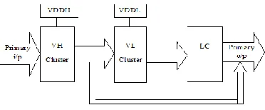
In order properly to assign VDD to gates in a Dual-VDD system, the Cluster Voltage Scaling (CVS) scheme is usually adopted. The structure of CVS is shown in Fig 1. CVS results in the clustering of gates in two sets namely a set of gates at high VDD and a set of gates at low VDD. It applies a high supply voltage (VDDH) in critical paths to ensure high performance and low supply voltage (VDDL) in non-critical paths to reduce power consumption [2].
Since the critical path of the circuit is unchanged, transformation preserves the circuit performance. Thus, the circuit has reduced power consumption without degrading performance. However, the PMOS transistor of the VDDH block cannot be shut off completely if it is directly driven by the output of the VDDL block [1].
IJIRT 142611
INTERNATIONAL JOURNAL OF INNOVATIVE RESEARCH IN TECHNOLOGY102
A. Dual-VDD CVS simulation stepsThe multiple supply system provides a high-voltage supply for high-performance circuits and a low-voltage supply for low-performance circuits. As shown in Fig.2 the dual VDD CVS structure has a several simulation steps for reduce the power dissipation in digital IC [3].
Fig 2.Dual-VDD CVS Simulation steps
III.PREVIOUS WORK
A. Clocked Pseudo-NMOS Level Converting Flip-Flop (CPN-LCFF)
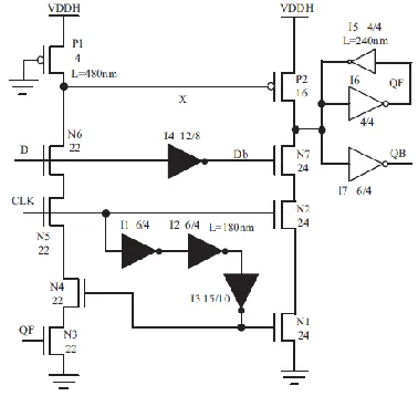
A clocked pseudo-NMOS level converting flip-flop (CPN-LCFF) proposed in [4] is shown in Fig.3, which is one of the most advanced single edge implicit pulse-triggered level converting flip-flops. An always on PMOS transistor P1 is used to charge node X so that it will not float when the LCFF is idle. It provides the feedback signal QF to eliminate the redundant discharge of node X. However, due to its implicit structure, there are too many stacked NMOS transistors in the discharging path (N3-N6) of node X. Since CLK and D are VDDL-swing signals, the widths of these NMOS transistors should be large enough to pull down the node X, will increase the overhead of power and area. Moreover, its inverter chain (I1-I3) is still switching with the clock when the input D remains the same.
Fig 3. Clocked Pseudo-NMOS Level Converting Flip-Flop (CPN-LCFF)
B. Level Converting Flip-Flop with Conditional Clock Technique (CC-LCFF)
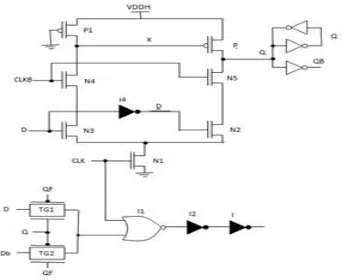
Clock-gating is used to block the clock when the input and output of the flip-flop remain the same, so the internal nodes will not make unnecessary transitions. CC-LCFF uses the output signal S of XNOR operation between D and Q to control the NOR gate I1.
When D is not equal to Q, S is “0”, I1 performs as an inverter, the CLK is not blocked and the low swing delayed clock signal CLKB is formed at output of I3, and the discharging paths (N1, N3, N4 and N1, N2, N5) perform properly. When D is equal to Q, S is “1”, the CLK is blocked by I1 and the output of I3 is “0”, the delayed clock signal CLKB is “0”, so the discharging paths (N1, N3, N4 andN1, N2, N5 ) do not perform and the inverters I2 and I3 will not switch the clock.
IJIRT 142611
INTERNATIONAL JOURNAL OF INNOVATIVE RESEARCH IN TECHNOLOGY103
Fig 4.Level Converting Flip-Flop with ConditionalClock technique
IV.POWER REDUCTION METHOD
Most of the memory elements are dynamic in nature, and some internal nodes are precharged and evaluated in each cycle without producing any useful activity at the output when the input is stable. Reducing the redundant switching activity has a profound effect in reducing the power dissipation. Many techniques are presented for reduce power dissipation.
The techniques are classified into three types Conditional precharge technique Conditional capture technique Conditional Discharge technique
Conditional Discharge Technique:
The clock-gating in the conditional capture technique results in redundant power consumed by the gate controlling the delivery of the delayed clock to the flip-flop. As a result, conditional precharge technique outperformed the conditional capture technique in reducing the flip-flop EDP. But the conditional precharge technique has been applied only to implicit flip-flop and it is difficult to use a double-edge triggering mechanism for these flip-flops, as it will require a lots of transistors. For this reason conditional discharge technique is used for applying this technique in both implicit and explicit pulse-triggered flip-flops without the problems associated with the conditional capture technique is proposed in [6]. The extra switching activity is eliminated by controlling the discharge path when the input is stable high by inserting NMOS transistor in the discharge path.
V.IMPLEMENTATION
The implementations are done inorder to compare the performance of the proposed level converting flip-flop with the previous works. Different level converting flip-flops are analyzed. Each circuit was designed by using Mentor graphics tool at 130nm technology.
A.Clocked Pseudo NMOS Level Converting Flip- Flop (CPN-LCFF)
The schematic and transient response of CPN LCFF are shown in Fig 5, 6 respectively. The data V(D) and CLK signal V(CLK) are given and the supply voltage of 5V. The output Q (B) is produces the output which is shown in Fig 6.
Fig 5. Schematic of Clocked Pseudo NMOS Level Converting Flip-Flop (CPN-LCFF)
IJIRT 142611
INTERNATIONAL JOURNAL OF INNOVATIVE RESEARCH IN TECHNOLOGY104
B. LCFF with Conditional Clock technique (CC-LCFF)
The schematic of CC-LCFF are shown in Fig 7 . The transient response is determined for 1GHz, 3GHz, 5GHz frequency which is shown in Fig 8,9,10 respectively.
Fig.7. Schematic of LCFF with a Conditional Clock technique (CC-LCFF)
Fig 8.Transient Response of 1 GHz frequency
Fig 9.Transient Response for 3 GHz frequency
3
G H z
f r e q u e n Fig 10.Transient Response for 5 GHz frequency
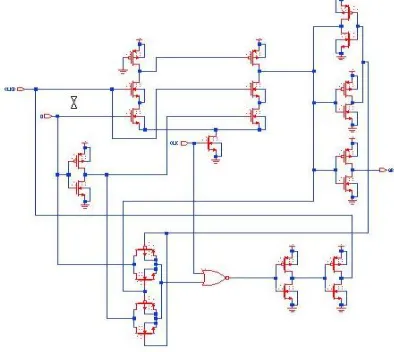
C. Proposed LCFF with Conditional discharge
Fig 11. Schematic of LCFF with conditional discharge technique
IJIRT 142611
INTERNATIONAL JOURNAL OF INNOVATIVE RESEARCH IN TECHNOLOGY105
The schematic and the transient response ofproposed LCFF with conditional discharge is shown in Fig 11, 12 respectively. In this NMOS transistor is inserted in-order to eliminate the switching activity.
Table I shows the power for various level converting flip-flop. When comparing with the other techniques the proposed LCFF with Conditional discharge technique consumes low power as 11.9116nW.
TABLE I
Design Name Power Delay
CPN-LCFF 1.1187mW 153.87ps
CC-LCFF 39.0718µW 385.22ps
Proposed LCFF 11.9116nW 381.81ps
Table I. Parameter Analysis
VI. CONCLUSION
Level converting Flip-Flop with Clocked pseudo NMOS, conditional clock and Conditional discharge techniques are stimulated in terms of power and delay. Their power are 1.1187mW, 39.0718μW, 11.9116nW.The proposed LCFF with conditional discharge technique consumes less power when comparing to other techniques. The power consumption is 11.9116nW and delay is 381.81ps.
REFERENCES
[1] P.M. Zeitzoff, J.E. Chung, A perspective from the 2003 ITRS: MOSFET scaling trends, challenges, and potential solutions, IEEE Circuits Syst. Mag. 21 (1) (2005) 4–15.
[2] Kulkarni S H & Sylvester D, 2004,‘High performance level conversion for dual VDD design’, IEEE Trans on Very Large Scale Integr (VLSI),Syst. Vol.12 (9) pp.926–936.
[3] F, Sheikh F & Nikolic B, 2004, ‘Level conversion for dual-supply systems’, IEEE Trans Very Large Scale Integr (VLSI) Sys., vol 12(2) pp.185–195.
[4] Zhao P, McNeely J B, Golconda P K, Venigalla S, Wang N, Bayoumi M B, Kuang W, & Downey L, 2009, ‘Low-power clocked pseudo NMOS flip-flop for level conversion in dual supply systems’, IEEE Transaction on Very Large Scale Integr. (VLSI) Syst. 17(9) 1196– 1202.
[5] Jizhong Shen n, Liang Geng, Guangping & Xiang Jianwei Liang, 2014, ‘Low-power level converting flip-flop with a conditional clock techniquein dual supply systems’, pp.857-863. [6] Peiyi Zhao, Bajoumi A,2004, ‘High-performance
and low-power conditional discharge flip-flop’,pp.477-484.
[7] Zhao P, Kumar G P, Archana C & Bayoumi M S, Feb 20 2004, ‘A double-edge implicit-pulsed level convert flip-flop’, Proceedings of the IEEE International Computer Society Annual Symposium on Very Large Scale Integration (VLSI), Los Angeles, USA, vol. 256, no. 12, pp. 141–144.
[8] Chiou L & Lou S, 2007, ‘An energy-efficient dual-edge triggered level-converting flip flop’, : Proceedings of the IEEE International Symposium on Circuits Systems, New Orleans, USA, pp. 1157–1160.
[9] Meimand H M & K.Roy,2004, ‘Dual edge triggered level converting flip-flops’, : Proceedings of the IEEE International Symposium on Circuits Systems, Canada, 2004, vol.2, pp. 661–664.