e-ISSN: 2250-3021, p-ISSN: 2278-8719
Vol. 3, Issue 9 (September. 2013), ||V3|| PP 39-51
Performance Analysis of Circular Microstrip Patch Antenna
With Dielectric Superstrates
V. Saidulu, K.Kumara Swamy, K.Srinivasa Rao
,P.V.D.Somasekhar Rao
1
Department of Electronics and Communication, MGIT,Hyderabad, AP, India 2
Department of Electronics and Communication, BIET, Hyderabad, AP, India 3
Department of Electronics and Communication, VIF,Hyderabad, AP, India 4
Department of Electronics and Communication,JNTUH,Hyderabad,AP,India
Abstract: - This paper demonstrates, the effect of dielectric superstrates on the performance of coaxial probe fed circular patch microstrip antenna with and without dielectric superstrates. The antenna can be designed at 2.4 GHz(ISM band) frequency and fabricated on Arlon diclad substrate, whose dielectric constant ( is 2.2. The theoretical formulation has been studied using cavity model analysis. In this paper experimentally studied the effect of dielectric superstrates on the parameters such as bandwidth, beam-width, gain and resonant frequency, input impedance, VSWR, return-loss etc. Measured results shows when placing the superstrate material above the substrate the antenna parameter will be changed and antenna resonant frequency will be shifted lower side, while other parameters have slight variation in their values. In particular, the resonant frequency increases with the dielectric constant of the superstrates. In addition, it has also been observed that return loss and VSWR increases, however bandwidth and gain decreases with the dielectric constant of the superstrates.
Keywords: - Circular Microstrip patch, Dielectric Superstrates, Resonant frequency, Bandwidth etc.
I. INTRODUCTION
Circular patch microstrip antennas are becoming a popular for portable wireless system because they are light weight, low cost, low volume, easily manufacturable and also other characteristic such as low profile and conformable due this reason antenna can use airborne and spacecraft application. In several application circular patch microstrip antenna and arrays require a dielectric superstrate over radiating elements to provide protection from heat, rain, physically damaged and naturally formed(ice layers) during flight or severe condition[1], [2]. The antenna usually placed beneath plastic cover or protective dielectric superstrate. Such dielectric superstrate over microstrip antenna shift the resonant frequency and also slight changing the values of other parameters such as bandwidth, beam-width, gain etc. Several researchers have studied the effect of dielectric superstrate on the resonant frequency of circular microstrip patch antenna [1] - [24] with numerical method. All of this method is complex and time consuming. This paper experimentally investigated the effect of dielectric superstrates with and without on the performance characteristics of circular microstrip patch antenna such as bandwidth, beam-width, gain, resonant frequency etc. The obtained results shows that the resonant frequency will be shifted to lower side by placing superstrate above substrate, while other parameter have slight variation in their values. In particular, the resonant frequency increases with dielectric constant of the superstrates. In addition, it has also been observed that the return loss and VSWR increase, however bandwidth and gain decreases with the dielectric constant of the superstrates.
II. ANTENNA SPECIFICATION AND SELECTION OF SUBSTRATE MATERIALS
for the substrate will be increase the fringing field of the patch and thus the radiated power. A high loss tangent (tan increases the dielectric loss and therefore reduce the antenna performance. The low dielectric constant materials increase efficiency, bandwidth and better for radiation.
Figure 1: Circular microstrip antenna
.
Figure 2: Structure of circular patch antenna
Figure 3: Circular microstrip antenna with probe feeding (8)
III. THEORITICAL FORMULATION
The circular microstrip antenna can be analyzed using cavity model in cylindrical coordinates [18]. The cavity is composed of two perfect electric conductors at top and bottom to represent the patch and the ground plane.
3.1. Electric and magnetic fields:
To find the fields with in the cavity, use the vector potential approach. For TM mode analysis need to calculate maganetic vector potential . The cylindrical coordinates the homogeneous wave equation of
(1) The electric and magnetic fields related to the vector potential [18]
, , ,
(2) Subject to the boundary conditions of
, (3)
The magnetic vector potential reduces to [18]
With the constraint equation of
(5)
The primed cylindrical coordinates are used to represent the fields with in the cavity while the Bessel function of the first kind of order m, and (6)
(7)
m= 0, 1, 2… (8)
n= 1, 2, 3… (9)
p= 0, 1, 2… (10) In represents the zeros of the derivative of the Bessel function , and they determine the order of the resonant frequencies. The first four values of , in ascending order, are (11)
3.2. Resonant Frequencies: The resonant frequencies of the cavity, and thus of the microstrip antenna, are found [5] – [10]. Since for most typical microstrip antennas the substrate height is very small (typically h 0.05 ), the fields along z are essentially constant and are represented in (10) by p= 0 and in (7) by . Therefore the resonant freqencncies for the modes can be written using (5) as (12)
Based on the values of (11), the first four modes, in ascending order, are whose resonant frequency is (13)
Where is the speed of light in free space. The resonant frequency of (13) does not take into account fringing. As was shown for the rectangular patch. Fringing makes the patch look electrically larger. The circular patch a correction is introduced by using an effective radius . (14)
Therefore the resonant frequency of (13) for the dominant should be modified by using (14) and expressed as (15)
3.3. Resonant input impedance: The input impedance of a circular patch antenna at resonance is real and the input power is independent of the feed point position along the circumference. Taking the feed as a reference point, the radial distance from the center of the patch for the dominant mode is [3]: (16)
Since the resonant input impedance of a circular patch with coaxial probe fed is expressed as[18]: = (17)
3.4.Fields radiated: Applying the Equivalence principle to the circumferential wall of the cavity, the equivalent maganetic current density can be obtaind and assuming a mode the field distribution under the patch. Since the thickness of the substrate is very small, the filamentary maganetic current becomes[12]: (18) Using equation( 5), the patch antenna can be treated as a circular loop and using the radiation equation the expression is given[3] (19)
(21)
IV. DESIGN OF CIRCULAR MICROSTRIP PATCH ANTENNA
Based on the cavity model formulation, a design procedure is outlined which leads to practical designs of circular microstrip antennas for the dominant mode. The procedure assumes that the specified information includes the dielectric constant of the substrate ( ),the resonant frequency( ) and height of the substrate h.
4.1. Circular patch radius and effective radius:
Since the dimension of the patch is treated a circular loop, the actual radius of the patch is given by (Balanis, 1982)
a= (22)
Where F =
Equation (1) does not take into considerations the fringing effect. Since fringing makes the patch electrically larger, the effective radius of patch is used and is given by (Balans, 1982)
(23)
Hence, the resonant frequency for the dominant is given by (Balanis,1982) (24)
Where vo is the velocity of light
V. MICROSTRIP ANTENNAS WITH DIELECTRIC SUPERSTRATE
5.1. Superstrate (radome) effects:
A circular microstrip patch may be subjected to icing or be coated with paint or other dielectric material for protection. These coatings affect performance of the microstrip antenna. In particular, the resonant frequency is lowered, causing tuning problems and severally degrading performance, which may serious, as the bandwidth of antenna is inherently low. When circular microstrip is covered with the dielectric superstrate or radome is shown in Figure 4, the characteristic impedance, phase velocity, losses, and Q factor of the line change as a function of the dielectric superstrate layer. The properties of a microstrip antenna with dielectric superstrate layer have been studied with the cavity model. The resonant frequency of a microstrip antenna covered with dielectric superstrate layer can be determined when the effective dielectric constant of the structure is known [8]. The change of the resonant frequency by placing the dielectric superstrate has been calculated using the following the expression [1].
(25)
If and , then
Where,
= Effective dielectric constant with dielectric superstrte =Effective dielectric constant without dielectric superstrate
Change in dielectric constant due to dielectric superstrate Fractional change in resonance frequency
Figure 4: Circular microstrip antenna with superstrate
VI. RESULT AND ANALYSIS
6.1. Experimental measurement:
The geometrical structure under consideration of circular patch antenna prototype and superstrate material is shown in Figure 6, Figure 7, Figure 8, Figure 9. A circular patch of radius is 47.1mm on thick substrate with a dielectric constant 2.2 was fabricated. The patch was fed through probe of 50Ω cable. The location of feed probe had been found theoretically and chosen as X=0, Y= 5.5mm. Then the patch was covered with different thickness of the dielectric superstrate material such as (1) Arlon Diclad 880 whose dielectric constant ( is 2.2, loss tangent (tan is 0.0009 and thickness ( ) is 1.6mm. (2) Arlon Ad 320 whose dielectric constant ( is 3.2, loss tangent (tan is 0.003 and thickness ( ) is 3.2mm. (3) FR4 whose dielectric constant ( is 4.8, loss tangent (tan is 0.02 and thickness ( ) is 1.6mm. (4) Arlon Ad 1000 whose dielectric constant ( ) is 10.2, loss tangent (tan is 0.0035 and thickness ( ) is 0.8mm. The impedance characteristics were measured by means of HP 8510B network analyzer is shown in Figure 5. The radiation pattern measurements were performed in the anechoic chamber by the use of automatic antenna analyzer.
Figure 5: Fabricated microstrip antennameasurements
Figure 6: Fabricated Porto type rectangular patch with feed point location
Figure 8: Dielectric superstrate is 3.2 and superstrate materials is 4.8
Figure 9: Dielectric superstrate is 10.
VII. RESULT OF CIRCULAR PATCH ANTENNA
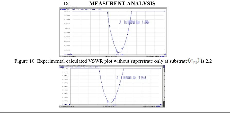
In order to present the design procedure of circular patch antenna achieving impedance matching for the case, the first prototype of the antenna was designed using Arlon diclad 880 substrate resonating at 2.4GHz and corresponding the results are shown in Fig. The obtained results show that the value of VSWR is 1.565 and Bandwidth is 3GHz, the Gain is 6.7dB and half power beam-width (HPBW) is .in HP and in VP, input impedance is 60.696Ω and return loss is -15.558 is shown in Figure 10, Figure 15, however the corresponding data are tabulated is shown in Table 5, Table 7, Table 9, Table 10 and Table 12.
VIII. RESULT OF CIRCULAR PATCH ANTENNA WITH VARIOUS DIELECTRIC
CONSTANTS
In order to observe the effect of dielectric supersrtrates on the antenna characteristics such as bandwidth, beam-width, gain and resonant frequency etc. The proposed antenna has been analyzed using various dielectric superstrates of dielectric constant is 2.2, 3.2, 4.8, 10.2, corresponding frequency will be shifted 2.40GHz,2.32GHz,2.33GHz,2.33GHz. The obtained charactestics are shown in Fig. The Gain is varied from 1.5Db to 4.8dB,Bandwidth is varied from2.2 GHz to 3.0GHz, input impedance is varied from 35.756Ω to56.112Ω, HPBW is constant in HP i.e is and in VP is varied from to is shown in Figure 10 to Figure 29 , however the corresponding data are tabulated in Table 6, Table 8, Table 11 and Table 12.
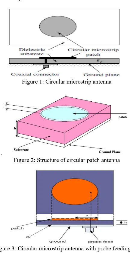
IX. MEASURENT ANALYSIS
Figure 11: Experimental calculated VSWR plot with superstrate is 2.2
Figure 12: Experimental calculated VSWR plot with superstrate is 3.2
Figure 13: Experimental calculated VSWR plot with superstrate is 4.8
Figure 14: Experimental calculated VSWR plot with superstrate is 10.2
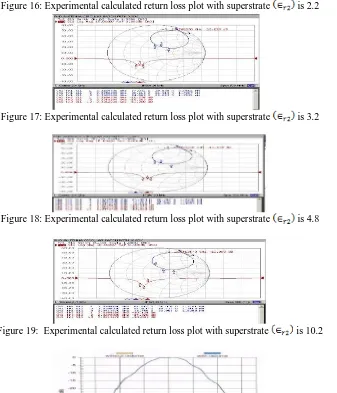
Figure 16: Experimental calculated return loss plot with superstrate is 2.2
Figure 17: Experimental calculated return loss plot with superstrate is 3.2
Figure 18: Experimental calculated return loss plot with superstrate is 4.8
Figure 19: Experimental calculated return loss plot with superstrate is 10.2
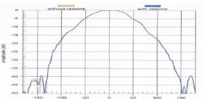
Figure 20: Experimental calculated far field amplitude of 2.4GHz radiation pattern plot without superstrate (radome) at VP
Figure 22: Experimental calculated far field amplitude of 2.4GHz radiation pattern plot with and without superstrate (radome) at is 2.2 at VP
Figure 23: Exprimental calculated far field amplitude of 2.4GHz radiation pattern plot with and without superstrate (radome) at is 3.2 at VP
Figure 24: Experimental calculated far field amplitude of 2.4GHz radiation pattern plot with and without superstrate (radome) at is 3.2 at VP
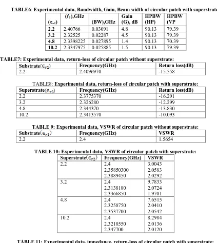
Figure 25: Experimental calculated far field amplitude of 2.4GHz radiation pattern plot with and without superstrate (radome) at is 4.8
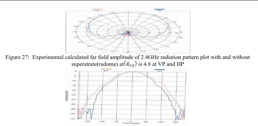
Figure 27: Experimental calculated far field amplitude of 2.4GHz radiation pattern plot with and without superstrate(radome) at is 4.8 at VP and HP
Figure 28: Experimental calculated far field amplitude of 2.4GHz radiation pattern plot with and without superstrate (radome) at is 4.8 at VP and HP
Figure 29: Experimental calculated far field amplitude of 2.4GHz radiation pattern plot with and without superstrate (radome) at is 10.2 at VP
Figure 30: Experimental calculated far field amplitude of 2.4GHz radiation pattern plot with and without superstrate (radome) at is 10.2 at VP
X. EXPERIMENTAL CALUCLATED DATA
TABLE 1: Selection substrate material for designing of circular microstrip a patch antenna: Substrate material Dielectric constant( Loss tangent(tan ) Substrate thicknes(h1),
mm
Arlon diclad 880 2.2 0.0009 1.6
TABLE2:Selection superstrate material for designing of circular microstrip a patch antenna: Superstrate Material Dielectric Constant ) Loss Tangent ( Superstrate
thickness ( ),mm
Arlon diclad 880 2.2 0.0009 1.6
Arlon Ad 320 3.2 0.003 3.2
FR4 4.8 0.02 1.6
Arlo Ad 1000 10.2 0.0035 0.8
Type of Patch Diameter(mm) Feed Point(mm)
Circular patch antenna 47.1 5.5
TABLE 5:Experimental data, Bandwidth, Gain, Beam width of circular patch without superstrate:
( ),GHz Band width,GHz Gain (G), dB HPBW (HP) HPBW (VP) 2.2 2.40766 0.03091 6.7/4.11 98.77 90.13
TABLE6: Experimental data, Bandwidth, Gain, Beam width of circular patch with superstrate:
( ) ( ),GHz (BW),GHz Gain (G), dB HPBW (HP) HPBW (VP 2.2 2.40766 0.03091 4.8 90.13 79.39 3.2 2.32525 0.02287 4.5 90.13 79.39 4.8 2.3398225 0.027895 1.4 90.13 70.39 10.2 2.3347975 0.025885 1.5 90.13 79.39
TABLE7:Experimental data, return-loss of circular patch without superstrate:
Substrate Frequency(GHz) Return loss(dB)
2.2 2.4096970 -15.558
TABLE8: Experimental data, return-loss of circular patch with superstrate:
Superstrate Frequency(GHz) Return loss(dB)
2.2 2.3775370 -16.291
3.2 2.326280 -12.299
4.8 2.344370 -13.830
10.2 2.3413570 -10.093
TABLE 9:Experimental data, VSWR of circular patch without superstrate:
Substrate Frequency(GHz) VSWR
2.2 2.4 1.5654
TABLE 10: Experimental data, VSWR of circular patch with superstrate: Superstrate Frequency(GHz) VSWR
2.2 2.4
2.35850300 2.3889450
3.0043 2.0583 2.0292
3.2 2.4
2.3138180 2.3366850
9.7833 2.0724 1.9701
4.8 2.4
2.3258750 2.3537700
7.6515 2.0410 2.0542
10.2 2.4
2.3218550 2.347700
8.2984 2.0136 2.0120
TABLE 11: Experimental data, impedance, return-loss of circular patch with superstrate: Substrate( Frequency(GHz) Impedance(Ω) Return loss(dB)
2.2(without) 2.40 60.696 -15.558
2.2 2.377 56.112 -16.291
3.2 2.326 54.985 -12.299
4.8 2.344 52.198 -13.830
10.2 2.341 35.756 -10.093
The measurement results carried out for the circular microstrip patch antenna can be designed at 2.4GHz and fabricated on Arlon ad 880 substrate, whose dielectric constant is 2.2. In this paper experimentally carried out with and without dielectric superstrates on the parameter such as gain, bandwidth,beam-width, resonant frqency etc.The result obtained only microstrip patch without superstrate is gain(G) is 6.7dB, Bandwidth(BW) is 3 GHz ,half power beam-width(HPBW) is in horizontal polarization and in vertical polarization, input impedance is60.696Ω, voltage standing wave ratio(VSWR) is 1.565 and return loss(RL) is -15.558dB.The microstrip patch with superstrates, the frequency will be shifted lower side from 2.4GHz to 2.32 GHz, Gain is varied from 1.4db to 4.8dB, the Bandwidth isvaried from 1GHz to 3GHz, VSWR is varied 2.583 to 2.013, return loss varied from -10.093 db to -16.291 dB and half power beam- width(HPBW) is constant in horizontal polarization i.e. is around and beam width is increase in vertical polarization based on thickness of dielectrc superstrates i.e. from to . The highest gain is obtained at microstrip patch with dielectric superstrate, whose dielectric constant is 2.2 at gain is 4.8dB and return loss is -16.291 dB is shown in Figure 10 to Figure 19 and corresponding data table can be tabulated is shown in Table 1 to Table 11.
XI. CONCLUSION
The design and development of circular microstrip patch antenna with and without dielectric superstrates presented. In this paper experimentally studied the effect dielectric superstrates with and without on the parameters such as bandwidth, beam-width, gain and resonant frequency etc. The result obtained only microstrip patch without superstrate is gain is 6.7dB, Bandwidth is 3 GHz,half power beam-width is in horizontal polarization and in vertical polarization,voltage standing wave ratio(VSWR) is 1.565, input impedance is 60.696Ω and return loss(RL) is-15.558. The microstrip patch with superstrates, the frequency will be shifted lower side from 2.4GHz to 2.32 GHz, Gain varying from 1.5dB to 4.8dB, Bandwidth varying from 2.2GHz to 3.0GHz, VSWR is varied from 2.013 to 2.583, return loss varying from -10.093db to -15.558 dB and half power beam- width is constant in horizontal polarization i.e around and half power beam-width in vertical polarization is varied from to based on the thickness of the dielectric superstraes, input impedance is varied from 35.756Ω to 56.112Ω. The highest gain is obtained at microstrip patch with dielectric superstrate , whose dielectric constant( is 2.2 at gain is 4.8dB and return loss is -13.635 dB is shown in Figure 10 to Figure 29 and corresponding data table can be tabulated is shown in Table 1 to Table 11. We observed experimentally results which are showing the variation of VSWR with different dielectric superstrate (radome) thickness, as dielectric superstrate thickness increases, VSWR increases. The variation of the antenna gain at different dielectric superstrate thickness as dielectric superstrate thickness increases, the gain decreases. The bandwidth of the microstrip antennas can also increases with increasing thickness of the dielectric superstrate for low dielectric constant materials, and decreases for high dielectric constant of the substrate materials. Initially the return loss increases with increasing thickness of dielectric superstrates and then decreases. The antenna beam width in vertical polarization increased from to and is constant at horizontal polarization is around ..
REFERENCES
[1] I J Bhal and P Bhartia, “Microstrip antennas”, Artech house, 1980.
[2] R.Shavit,”Dielectric cover effect on Rectangular Microstrip Antennas array”. IEEE Trans. Antennas propagat.,Vol 40,. PP.992-995, Avg.1992.
[3] Inder ,Prakash and Stuchly, “Design of Microstrip Antennas covered with a Dielectric Layer. IEEE Trans. Antennas Propagate. Vol.AP-30.No.2, Mar 1992.
[4] O.M.Ramahi and Y.T.LO, ”Superstrate effect on the Resonant frequency of Microstrip Antennas”, Microwave Opt.Technol. Lett. Vol.5, PP.254-257,June 1992.
[5] A.Bhattacharyya and T. Tralman, “Effects of Dielectric Superstrate on patch Antennas”, Electron Lett., Vol.24,PP.356-358, Mar 1998.
[6] R.Afzalzadeh and R.N.Karekar, ”Characteristics of a Rectangular Microstrip patch Antenna with protecting spaced Dielectric Superstrate”, Microwave Opt. Technol. Lett., Vol.7, PP.62-66, Feb 1994. [7] I J Bahl P. Bhartia, S.Stuchly “ Design of microstrip antennas covered with a dielectric layer. IEEE
Trans. Antennas Propogat. No. 30, PP. 314-318, Mar 1982
[8] Odeyemi KO, Akande, D.O and Ogunti E.O.” Design of S-band Rectangular Microstrip Patch Antenna, European Journal of Scientific Research Volume 55, Issue 1, 2011
[9] Bernnhard and Tousignant, “Resonant Frequencies of rectangular microstrip antennas with flush and spaced dielectric superstrates”, IEEE Trans. Antennas Propagat, vol.47, no.2, Feb 1999.
[11] P. Malathi AND Rajkumar” Design of multilayer rectangular microstrip antenna using artificial neural networks” International journal of recent trends in Engineering, vol.2, no.5, Nov. 2009.
[12] P. Malathi and Rajkumar “On the design of multilayer circular microstrip antenna using artificial neural network”, International Journal of Recent Trends in Engineering, vol.2, No.5, Nov. 2009.
[13] Christopher J Meagher and Satish kumar Sharm “ A wide band aperture- coupled microstrip patch antennas employing space & dielectric cover for enhanced gain performance, IEEE Transaction on antenna and propagation, Vol.58, No.9, Sep. 2010.
[14] Bahl, I.J, Stuchly, S.S, “Analysis of a microstrip covered with a lossy dielectric, IEEE Trans. Microwave Theory Tech., 28, pp.104-109.1980.
[15] Alexopoulos N.G.Jackson, D.R. “Fundamental superstrate (cover) effects on printed antennas, IEEE Trans. Antennas Propagat.32, PP. 807-816.
[16] R. Garg, P. Bhartia, I. Bahl, and A. Ittipiboon, Microstrip Antenna Design Hand book, Artech House, Canton, MA, 2001
[17] Balanis, C.A., Antenna Theory: Analysis and Design, John Wiley& Sons.
[18] James J.R., and Hall P.S, Handbook of microstrip antennas, peter Peregrinus, London, UK, 1989. [19] R.K.Yadav,R.L.Yadava “Performance Analysis of superstrate loaded patch antenna and Abstain from
environmental Effects”International Journal of Engineering science and Tech., vol.3, no.8, p.p.6582-6591, Aug. 2011.
[20] R.K.Yadav and R.L.Yadava “Effect on performance characteristics of rectangular patch antenna with varying height of dielectric cover” International Journal of power control signal and computation, vol.1, no.1, p.p.no.55-59.
[21] Samirdev Gupta, Amit singh “Design and Analysis of multidielectric layer microstrip antennas with superstrate layer characteristics” International Journal of Advances in Engg & Tech., vol.3,issue1, p.p no.55-68
[22] Rajkumar P.Malathi and J.P. Shinde “ Design of circular microstrip patch with spaced dielectric superstrates” IEEE, P.P.NO.315-317, 2007.