Low
Am
Abstract circuit. T designin analog c using 18 56.88% low volta range of
Keyword
Analog c complica operate o transcond device w voltages conversio The outp Where V
the trans (2) Where tr area. W Operation symbol transcond the ampl excess ph Operation designing
w Pow
mplifie
t- Low Powe This is the m
g of the low p circuit opera
0nm technolo from the sup age low powe f 1 GHz.
d- Bulk driven
circuit is the ated than the d on only 0 and ductance amp where input is
at the input on device. On put current is c
Vin+ is the volt sconductance
rasconductanc
is the effectiv nal transcond
of the oper ductance of th lifier's transco hase issues, fl
nal Trranscon g of low powe
wer O
er Des
E National Inst E National Inster and low v main issue fo
power analog ation. In this ogy at the su pply voltage v
er operationa
n Transistor, C
basic fundam digital design. d 1. One of th plifier (OTA)1
taken in form terminal is u ne additional in
calculated as f tage at the
of the amplif
ce parameter k
ve channel le ductance ampl rational tranc he amplifier. I onductance. T exibility and t
Fig
nductance Am er circuit. It is
Operat
sign u
Electronics & titute of Teach pritigupta
R
Electronics & titute of Teach
voltage circu or the VLSI c
g circuit. Bul paper low v pply voltage varies from 1 al transcondu
CMOS techno
1.
mental block o Analog circu he most impor
. Operational m of voltage used to produ
nput is applied follows:
I non‐inverting fier. gm is trans 2kI
k= µCox W/2L ngth. Ideally ifer has high conductance
Iabc is called a The advantage tunability and
g.1 Symbol of Op
mplifier has m s used in desig
tional
using
Priti Gupta Communicati her’s Training a23091989@g Rajesh Mehr Communicati her’s Training uit designing circuit design k driven tech voltage oper1.5V to 0.9V 1.5V to 0.8 V uctance amp
logy, Moore’s
Introducti
of the Electro uit operates on rtant and wid Tranconducta and output is ce current at d to the tranco
V -V g
g input, Vin− is sconductance
L, µ is the mo operational tr input impeda amplifier. Iab amplifier bias es of OTAs in d realization of
perational Tranco
many applica gning of activ
l Tran
180nm
ion departmen g and Research
gmail.com
ra
ion departmen g and Research
is the critic ning area. T hnique is the ational trans V. Results hav V. Simulation lifier for the
s Law, VLSI.
ion
onics Enginee n continuous v dely used anal ance Amplifie s taken in for the output. S onductance am
g s the voltage gain is given
obility of the ranconductan ance and high
bc input bias current of the nclude large b f high integrat
onductance Ampli
ation in the ve filters, porta
nscond
m Tec
nt h, Chandigarh nt h, Chandigarhcal issue for here is many power reduc sconductnce ve reduced th
results show high frequen
ering. Analog valued signal,
log building b er is a voltage rm of current. So it is basic mplifier to con
e at the inve
by:-
carrier, Cox is ce amplifier h output imped s current is e amplifier. I bandwidth, la tion level inte
ifier integrated ci able devices,
ducta
chnolo
h h the battery y techniques ction techniqu amplifier is he power con ws the designincy applicati
circuit design whereas digit block is the op e control curre
. The differen ally voltage t ntrol the outpu
erting input
s the capacito has infinite b dance. Fig. 1 s
used to co abc is directly arge dynamic grated circuits
ircuit such th sensor implem
nce
ogy
operated used for ue for the designed sumption ing of the ion in the
n is more tal circuits perational ent source nce of the to current ut current.
(1) and gm is
or per unit andwidth. shows the ontrol the
related to range, no s1.
hearing aid implementation. OTAs are versatile analog building blocks that allow the amplification and filtering of signals with minimum power consumption2.
1.1 Architecture of OTA
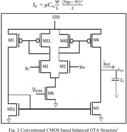
Low power System design depends on the topology of the OTA’s. The designing of the OTA suffers challenges of the supply voltage and channel length scale down with the advancement of new generation CMOS technology. Operational transconductance Amplifier is the main building block for the analog processing applications. The design challenges for the OTA are still present in terms of gain, power consumption and gain bandwidth product efficiency. The classification of the operational tranconductance amplifier is single ended output and differential ended output or fully differential OTA’s. The fully differential provides stable input common mode voltage and reduces the harmonic distortion. The realization of CMOS based OTA has resulted in low power and high performance, however, the era of CMOS is nearing its end1.The basic balanced OTA structure of the OTA based on CMOS is shown in fig. 2 where Vp and Vm are the non-inverting and inverting terminal of the OTA. The transistor M3 and M31 forms the current mirror. Similarly M4 and M41 form the current mirror. The W / L ratio of the transistor M3 and M31 are same and W / L ratio of the transistor M4 and M41 are same. It is desirable to operate all transistors in saturation region for the operation on operational tranconductance amplifier. For the operation of transistors in the saturation region it is required to maintain the condition Vgs>Vt and Vds >Vgs – Vt , Where the value of the current Id is such that
Id = µCox – (3)
Fig. 2 Conventional CMOS based balanced OTA Structure1
So the conduction of the current depends on the transistor sizing that is the value of the W/L.
2. Power Consumption
The power consumption refers to the total power consumption of the device and power dissipation is referred to the total power wasted through the undesirable components. The power dissipation is dependent on the supply
voltage and current. The power dissipation of the device is calculated easily from the total power dissipation and load power dissipation. Power dissipation is dependent on the load CL. In power dissipation, power is converted to heat and then radiated away from the device. then a better cooling mechanism would be required to keep the circuit in normal conditions. Also large power dissipation requires expensive and noise cooling machinery, batteries and power conservation circuits3. Due to this generated heat, device may get damaged on continuous use. Slew rate and unity gain frequency of the OTA depends on the value of the load capacitor. These factors are decreased with the increase of the value of load CL. conventional amplifiers require power supply voltages at least equal to the magnitude of the largest threshold voltages of the PMOS or the NMOS transistors plus necessary signal swing4. Power Consumption is the important parameter while designing any type of the integrated circuit. There is a trade of between the power and performance of the integrated circuit. The main aim of this paper is to maintain performance of the integrated circuit while reducing the power consumption because the cost of the system is dependent on the power. Power dissipation in CMOS circuits is the combination of three main components.
Static (leakage) power dissipation
Short circuit power dissipation
2.1 Static Power Dissipation
Static power dissipation is related to logical states of the circuits and it is independent of switching activities. The static power dissipation of a circuit is defined as the product of the device leakage current and the supply voltage. Total static power dissipation is-
P =I V (4) where Isat is the current that flows through the circuit when there is no switching event and V DD is the supply voltage.
2.2 Short Circuit Power Dissipation
Short-circuit power dissipation in CMOS inverter occurs for finite rise and fall times of input voltage waveforms. A direct current path is formed, When both NMOS and PMOS transistors are turned on in the circuit simultaneously for a short duration of time during switching, This causes a direct current path between powers supply and ground. During switching, the current does not contribute to the charging/discharging of capacitance and current components that flow through both PMOS and NMOS transistor are called short circuit components5.
2.3 Dynamic Power Dissipation
Dynamic power dissipation is the result of power dissipation during switching activity. A higher operating frequency leads to more switching activities in the circuits and results in increased power dissipation5. The most significant contributor to dynamic power dissipation in CMOS circuits is the charging/discharging of load capacitance. Consider the simple CMOS inverter and assume that a step voltage with negligible rise and fall time is applied.When input voltage switches from 0-V DD, load capacitance in this duration is being discharged through NMOS transistor as the NMOS transistor starts conducting and PMOS transistor is turned off. Thus, the current in load capacitance is equal to the instantaneous drain current of the NMOS transistor.
3. Technology Scaling
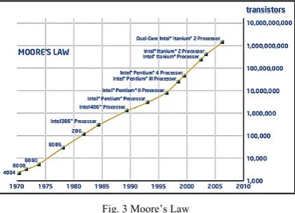
With the advancement of the low power battery operated portable devices, technology scaling is the main requirement for the electronic industry. Transistor manufactured now a days are faster than the transistors manufactured 20 years back. They also require less area. So chip size reduces. The reduction of minimum dimensions in CMOS technologies necessitates the downscaling of power supply voltage accordingly in integrated circuits (ICs)6. Modern CMOS technology downscales, the reduction of supply voltage in CMOS integrated circuits has led to smaller common-mode input range for traditional operational amplifiers (OpAmp) with a single input differential pair and a reduced signal-to-noise ratio7. Scaling down the transistor sizing has provided the technology such as 180nm, 90nm and 45nm. Is is difficult to scale the transistor from 60nm to the lower range due to the short channel effects and reliability factor. New efficient materials and devices need to be found to replace the existing silicon based MOSFETs and provides enhancement in the Moore’s Law. Low Voltage operation and optimized power-to-performance ratio are required by modern wireless and portable electronics in order to decrease battery weight and size and to extend battery lifetime8. The demand of these devices depends on various factor such that higher speed, lower delay, low area, low power consumption, small silicon area, longer battery life and high realibility9.
Fig. 3 Moore’s Law
technologies to nanometer dimensions has resulted in reduced headroom for analog operation3. Moreover, short channel effects such as drain induced barrier lowering have decreased the drain-source impedances reducing the transistor’s intrinsic gain3.Usually, the transistor sizing problem in integrated circuit design is solved using manual design and circuit simulators, some structure specific optimizers11. Today leakage power has become an increasingly important issue in processor hardware and software design5. With the main component of leakage, the sub-threshold current, exponentially increasing with decreasing device dimensions, leakage commands an ever increasing share in the processor power consumption10.
4. Bulk Driven Technique
Generally terminal of the MOSFET is used while designing the analog circuit with the help of the CMOS technology. MOSFET has one more terminal called bulk terminal or body terminal that is not used usually. Bulk Driven (BD) technique is developed for the use of body terminal as the fourth terminal. Input is applied to the body terminal instead of the gate terminal. Bulk-driven circuits are typically used to overcome issues of poor signal swing in such cases3, 4. Bulk driven technology can be implemented on the NMOS transistor but it suffer from the low transconductance amplifier. So It is better to use bulk driven technology on the PMOS transistor. Bulk driven technology is basically used to provide the low operating input range. It reduces the threshold voltage value that was fixed for the gate driven technology. The rail-to-rail differential input stage is commonly used to take advantage of the entire range of the power supply 18, 19. The operation of the Bulk-driven MOS transistor is much like a JFET i.e. a depletion type device, it can work under negative, zero, or even slightly positive biasing condition20.
5. Proposed Operational Transconductance Amplifier Design
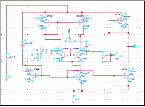
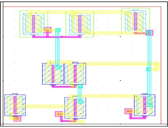
The schematic of the proposed bulk driven operational tranducdauctance amplifier is implemented with the help of 180nm technology shown in fig.4. Ibias current is 50µA for designing of the 2 stage operational. The layout of the bulk driven OTA is shown in fig. 5.
Fig. 4 Bulk driven Operational Transconductance Amplifier
Fig. 5 Bulk driven Operational Transconductance Amplifier Transient Response layout at Vdd=1.5V
5.1 Simulated Result on Vdd= 1.5V
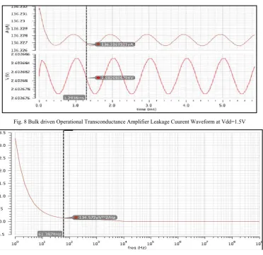
Fig. 6, 7, 8,and 9 shows the transient response, Power , Leakage current and Noise Wavefrom of operational Transconductance Amlipfer for the supply Voltage of 1.5V.
Fig..6 Bulk driven Operational Transconductance Amplifier Transient Response at Vdd=1.5V
Fig. 8 Bulk driven Operational Transconductance Amplifier Leakage Cuurent Waveform at Vdd=1.5V
Fig. 9 Bulk driven Operational Transconductance Amplifier Noise Response Waveform at Vdd=1.5V
5.2 Simulated Result on Vdd= 0.9V
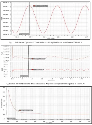
Fig. 10, 11,12 ,and 13 shows the transient response, Power, Leakage current and Noise Wavefrom of operational Transconductance Amlipfer for the supply Voltage of 0.9V
Fig. 11 Bulk driven Operational Transconductance Amplifier Power waveform at Vdd=0.9 V
Fig.12 Bulk driven Operational Transconductance Amplifier leakage current Response at Vdd=0.9V
Fig. 13 Bulk driven Operational Transconductance Amplifier Noise waveform at Vdd=0.9V
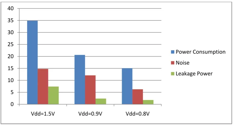
6. Simulation Result
Table 1 shows the performance parameter of bulk driven OTA for the low voltage range at 180nm technology Table 1
OTA Parameter
Bulk-Driven OTA at VDD=1.5 V
Bulk-Driven OTA at VDD=0.9 V
Bulk-Driven OTA at VDD=0.8 V
Power
consumption(pW) 34.88 20.61 15.04
Noise(V/µsec) 7.79X10⁻¹¹ 6.35 X10⁻¹¹ 3.186 X10⁻¹¹
Leakage Current(pA) 136.2 19.14 17.71
Fig. 14 Performance Parameter of the bulk driven OTA using 180nm
7. Conclusion
Table 1 shows that the power consumption is reduced with the reduction in the supply voltage from Vdd = 1.5V to 0.8V. Other parameter such as leakage current, leakage power and noise is reduced with the use of bulk driven technology. Bulk Driven technique is applied at the input stage of the operational transconductancce amplifier is used to reduce the threshold voltage requirement for the gate terminal. This effect causes the deduction in the leakage. So leakage current and leakage power is reduced. Bulk driven technique reduces the supply voltage required for the proper functioning of the operational transconductance amplifier for 180nm technology. Performance parameter is compared as shown in fig. 14 for the different supply voltage.
Acknowledgement
Authors would like to thank, Director, National Institute of Teacher Training and Research, Chandigarh for their inspiration, motivation and support throughout this research.
Reference
[1] Sajad A Loan, M. Nizamuddin, Faisal Bashir, Humyra Shabir, Asim. M. Murshid, Abdul Rahman Alamoud ,Shuja A Abbasi, “Design of a Novel High Gain Carbon Nanotube based Operational Transconductance Amplifier”, International MultiConference of Engineers and Computer Scientists”, Vol. 2, pp. 7-12,Mar. 2014.
[2] Joel Gak, Matías R. Miguez, Alfredo Arnaud, “Nanopower OTAs with Improved Linearity and Low Input Offset Using Bulk Degeneration”, IEEE Transaction on Circuit and Systems, Vol. 60, No. 5, pp. 1186-1174, May 2013.
[3] Siddharth Seth, Student, Boris Murmann, Senior, “Settling Time and Noise Optimization of a Three-Stage Operational Transconductance Amplifier”, IEEE Transsaction on circuits and sysytem, Vol. 60, No. 5 pp. 1168–1174, May. 2013.
[4] L. H. C. Ferreira, T. C. Pimenta, and R. L. Moreno, “An ultra-low-voltage ultra-low-power CMOS miller OTA with rail-to-rail input/output swing,” IEEE Trans. Circuits Syst. II, Exp. Briefs, vol. 54, no. 10, pp. 843–847, Oct. 2007.
[5] Omar Abdelfattah, Gordon W. Roberts, Ishiang Shih, Yi-Chi Shih, “An Utlra- Low Voltage CMOS Process-Insensitive Self-Biased OTA with Rail-to-Rail Input Range”, IEEE Transaction on Circuit and Systems, Vol. 62, No. 10, pp. 2380-2390, Oct. 2015.
[6] Liang Zuo, , Syed K. Islam S. O. Cannizzaro, A. D. Grasso, R. Mita, G. Palumbo, S. Pennisi, “Low-Voltage Bulk-Driven Operational Amplifier With Improved Transconductance”, IEEE Transaction on Circuits and Systems -1, Vol. 60, No. 8, pp. 2084–2091, Aug 2011.
[7] Shanshan Dai, Xiaofei Cao, Ting Yi, Allyn E. Hubbard, Zhiliang Hong, “1-V Low-Power Programmable Rail-to-Rail Operational Amplifier With Improved Transconductance Feedback Technique”, IEEE Transaction on very large scale integration systems, Vol. 21, No. 10, pp. 1928-1934,Oct. 2013.
[8] Antonio J. López-Martín, Sushmita Baswa, Jaime Ramirez-Angulo, Ramón González Carvajal, Senior, “Low-Voltage Super Class AB CMOS OTA Cells With Very High Slew Rate and Power Efficiency” IEEE Journal of Solid-State Circuits, Vol. 40, No. 5, pp. 1068-1077, May 2005.
[9] Anjali Sharma ,Rajesh Mehra, “Area and Power Efficient CMOS Adder Design by Hybridizing PTL and GDI Technique”, International Journal of Computer Applications, Vol. 66, No. 4, pp. 15-22, Mar. 2013
[10] Hemasundar Mohan Geddada, Chang-Tsung Fu, Jose Silva-Martinez, Stewart S. Taylor, “Wide-Band Inductorless Low-Noise Transconductance Amplifiers With High Large-Signal Linearity”, IEEE Transaction on Microwave Theory and techniques , Vol. 62, NO. 7, July 2014.
[11] H. Y. Koh, C. H. Sequin, and P. R. Gray, “OPASYN: A compiler forCMOS operational amplifiers,” IEEE Trans. Computer-Aided Design,vol. 9, pp. 113–125, Feb. 1990.
[12] Richa Singh,Rajesh Mehra, “Power Efficient Design of Multiplexer using Adiabatic Logic”, International Journal of Advances in Engineering & Technology ,Vol 6, pp. 246-254,Mar. 2013.
[13] B. J. Blalock, P. E. Allen, G. A. Rincon-Mora, “Designing 1-V Op Amps using standard digital CMOS technology,” IEEE Transaction on Circuits Systems, Analog Digit. Signal Process., vol. 45, no. 7, pp. 769–780, Jul.1998.
[14] E. D. C. Cotrim and L. H. C. Ferreira, “An ultra-low-power CMOS symmetrical OTA for low-frequency applications,” Analog Integrated Circuits Signal Process, vol. 71, no. 2, pp. 275–282, May 2012.
0 5 10 15 20 25 30 35 40
Vdd=1.5V Vdd=0.9V Vdd=0.8V
Power Consumption
Noise
[15] R. L. Geiger and E. Sanchez-Sinencio, “Active filter design using operational transconductance amplifiers: A tutorial,” IEEE Circuits Devices Mag., pp. 20–32, Mar. 1985.
[16] Jyoti , Rajesh Mehra, “Area Efficient Layout Design of CMOS Comparator using PTL Logic”, International Journal of Computer Applications, Vol. 122, No. 16, pp. 14-17, July 2015.
[17] Pushpa Saini, Rajesh Mehra, “A Novel Technique for Glitch and Leakage Power Reduction in CMOS VLSI Circuits”, International Journal of Advanced Computer Science and Applications, Vol. 3, No. 10, pp. 161-168, Oct. 2012.
[18] Pushpa Saini , Rajesh Mehra, “Leakage Power Reduction in CMOS VLSI Circuits”, International Journal of Computer Applications ,Vol. 55, No. 8 pp. 42-48, Oct. 2012.
[19] Rahul Sarpeshkar1, Richard F. Lyon2, Carver Mead,“ A Low-Power Wide-Linear-Range Transconductance Amplifier”, Springer Journal of Analog Integrated Circuits and Signal Processing, vol. 13, no.1, pp.123-151, May 1997.
[20] Giuseppe Ferri, Vincenzo Stornelli, Angelo Celeste,“Integrated Rail-to-Rail Low-Voltage Low-Power Enhanced DC-Gain Fully Differential Operational Transconductance Amplifier” ETRI Journal, vol.29, no.6, pp.785-793, Dec. 2007.