AN APPROACH TO DESIGN
ADVANCED STANDARD ENCRYPTION
ALGORITHM USING HARDWARE /
SOFTWARE CO-DESIGN
METHODOLOGY
MEGHANA A. HASAMNIS*
Associate Professor, Department of Electronics Engineering Shri. Ramdeobaba College of Engineering and Management, Nagpur, India
S. S. LIMAYE
Professor, Department of Electronics Engineering Jhulelal Institute of Technology, Nagpur, India
Abstract: An Advanced Standard Encryption Algorithm (AES) is widely used in modern consumer electronic products for security. The IEEE 802.15.4 Low-Rate wireless sensor networks also use AES algorithm where low power consumption is the priority. To reduce the time taken for encryption of huge data, the algorithm has to be implemented in hardware. To meet the requirement for low area the algorithm has to be implemented in software. Hence, a balance has to be achieved between hardware and software implementations in terms of area and speed, so as to improve the overall performance of the system. Also with the co-design methodology total thermal power dissipation is reduced. In this paper, 128 bit AES algorithm is implemented with hardware in combination with software using Altera NIOS II Processor platform. Altera’s Quartus II environment is used for design of the system. Cyclone II FPGA is used as a development platform. Software program is written in C language. NIOS II Integrated Development Environment (IDE) is used to integrate hardware and software together. By adopting hardware / software co-design methodology for implementation of AES, results show that a considerable improvement in speed can be achieved as compared to software only approach. Further, the significant reduction in area is achieved as compared to hardware only approach. By the approach of co-design an optimized design in terms of speed and area is achieved and also the thermal power dissipation is reduced.
Keywords: AES, Hardware / Software Co-design, NIOS II Processor, NIOS II IDE, Cyclone II FPGA.
1. Introduction
In 2001, the National Institute of Standards and Technology (NIST) adopted the Rijndael algorithm as the Advanced Encryption Standard (AES) [3]. The AES algorithm started immediately replacing the data encryption standard (DES), which had been in use since 1976. AES outperforms DES in improved longterm security because of larger key sizes (128, 192, and 256 bits). Another major advantage of AES is the efficient implementation on various platforms. AES is suitable for small 8-bit microprocessor platforms and common 32-bit processors. AES can be implemented in hardware and software both. Although AES is used in many different applications, hardware implementation of the algorithm focuses mostly on throughput optimization [4].
As compare to software implementation, hardware implementation provides greater physical security and higher speed. Software, on the other hand, is slower but much more flexible, and realizes the required functionality. Any modification can be easily done in an editor, and after re-compilation, the software provides the new functionality. The combination of hardware and software works very well in AES application.
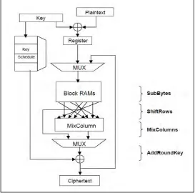
This paper gives the implementation of AES algorithm using hardware / software co-design methodology. AES algorithm comprises of four different blocks which are sequentially implemented. The different blocks are Addroundkey, Subbytes, Shiftrow and Mixcolumn, each block performing its own specific task. Firstly, the complete AES is implemented in software and the time taken for execution of each block is calculated. Secondly, each individual block is kept in hardware and time taken for execution of each block in hardware is calculated. The Subbytes block consumed maximum time in software i.e. critical part in software and minimum time in hardware as compared to other blocks. Hence an AES algorithm was designed keeping one block Subbytes in hardware and remaining blocks i.e. Addroundkey, Shiftrow and Mixcolumn in software. The results showed a considerable increase in speed as compared to software and reduction in area as compared to hardware implementation. Total thermal power dissipation was also reduced.
2. Advanced Encryption Standard (AES) Algorithm
The standard algorithm comprises three block ciphers, AES-128, AES-192 and AES-256, adopted from a larger collection originally published as Rijndael. Each AES cipher has a 128-bit input block size, with key sizes of 128, 192 and 256 bits, respectively. The AES ciphers have been analyzed extensively and are now used worldwide. The AES algorithm organizes the data block in a four-row and row-major ordered matrix [5]. The AES algorithm uses a round function.
The step involved are given below
1. Key Expansion using Rijndael's key schedule 2. Initial Round
- AddRoundKey 3. Round
- Sub Bytes: a non-linear substitution step where each byte is replaced with another according to a lookup table. - Shift Rows: a transposition step where each row of the state is shifted cyclically a certain number of steps. - Mix Columns: a mixing operation which operates on the columns of the state, combining the four bytes in each column.
- AddRoundKey: each byte of the state is combined with the round key; each round key is derived from the cipher key using a key schedule.
4. Final Round (no Mix Columns) - Sub Bytes
Fig. 1. Block Diagram of Encryption
3. The Hardware / Software Co-Design
3.1. FPGA Platform
With increasing device densities, difficult challenges become feasible and the integration of embedded SoPC (System on Programmable Chip) systems is significantly improved. Reconfigurable systems on a chip have become a reality with softcore processor. Softcore processor is a microprocessor fully described in software, usually in VHDL description, and capable to be synthesized in programmable hardware, such as FPGA. Softcore processors can be easily customized to the needs of a specific target application. The two major FPGA manufacturers provide commercial softcore processors; Xilinx offers MicroBlaze processor, also, Altera offers Nios II processors [6]. The benefit of a softcore processor is to add a micro-programmed logic that introduces more flexibility. A hardware / software co-design approach is then possible and a particular functionality can be developed in software for flexibility and upgrading completed with hardware custom blocks for cost reduction and performances.
3.2.Nios II Development Board
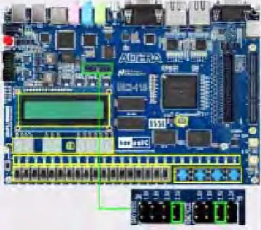
For software implementation of algorithms, the use of a microprocessor is required. The use of additional hardware for optimization contributes to the overall performance of the algorithm. For the highest degree of hardware / software integration, a softcore processor is used. For the main processing stage, the Altera NIOS II development board is used [7]. The core of the board is the Altera Cyclone II EP2C35F672C6 FPGA.
Fig. 2. Altera Cyclone II Development Board
3.3.Nios II CPU
The Altera NIOS II softcore processor (standard version) is a 32-bits scalar RISC with Harvard architecture, 5 stages pipeline, 1-way direct-mapped 64KB data cache, 1-way direct-mapped 64KB instruction cache and can execute up to 150 MIPS [8]. The softcore processor is used as it gives extensibility and adaptability. Directly a custom hardware device can be incorporated in the system. The custom logic helps to optimize the system for a specific application. Several peripheral devices and connectors UART, LCD, VGA and Ethernet etc. serve as interfaces between the Cyclone II FPGA and the external environment. For the embedded system, peripherals used are NIOS II Processor, URAT, Performance Counter, SRAM Controller, SRAM, PIO’s. In Altera’s Quartus II the SOPC builder tool is available. Using the SOPC builder tool the embedded system is designed quickly. Fig. 3. Shows the system design around NIOS II processor and the peripherals used.
Fig. 3. System design around NIOS II Processor
3.4.Timing Profile
In order to optimize and achieve best performance in terms of real-time operation of the AES algorithm, hardware / software co-design process is used [9][10]. At first, the algorithm was coded in C programming language on a PC platform. The tested software code was then rebuilt and transferred into the Nios II system. The performance analysis was done. The CPU clock cycles consumed by the four individual blocks of the AES algorithm were calculated. The total time taken for encryption was calculated. The software critical parts in the algorithm were detected and were implemented in hardware in VHDL language.
JTAG URAT
AVALON BUS
PIO
NIOS II PROCESSOR
SRAM CONTROLLER
3.5.Hardware Implementation
The critical parts of the AES algorithm which were detected from the timing profile were implemented in hardware and written in VHDL language. From the results it was found that the maximum CPU cycles were consumed by the subbytes block in the AES algorithm. The subbytes block was shifted in hardware and the remaining blocks are kept in software. The block shifted in hardware was connected with the NIOS II system through general purpose input and output (GPIO) as a custom hardware block to accelerate the encryption process. Two GPIO’s are used, one at input of subbytes and other at output of subbytes. The GPIO’s are of 32 bits and the AES algorithm is of 128 bits. The subbytes block is also of 128 bits and hence a demultiplexer is used at the input and a multiplexer is used at the output. Fig. 4. shows hardware implementation of subbytes.
Fig. 4. Hardware Implementation of Subbytes
4. Implementation Results
The encryption algorithm was succesfully run in software and the CPU cycles were calculated for each block of the AES algorithm. Later ever block of the algorithm was shifted in hardware individually and input and output was given through software. The CPU cycles were calculated for every block in hardware. The blocks shifted in hardware were connected with the system through GPIO and results obtained on the console window in NIOS II IDE. The plain text of 128 bits is given as the input along with the cipher key of 128 bits. This encrypted data is send to the PC through JTAG URAT to analyze the results. The ‘Table I,’ shows the results obtained in terms of CPU cycles for all the blocks individually in hardware and software.
Table 1. CPU Cycles of all the blocks of AES Algorithm in Hardware and Software
Blocks of AES Algorithm
Total time (CPU Cycles) Software
Total time (CPU Cycles) Hardware
Addroundkey
134841 106178Subbyte
168231 25867Shiftrow
94818 28887Mixcolumn
109683 52504AES block interfaced with the Processor was compiled and the compilation results are presented in Table II. Table 2. Compilation results of AES
AES Algorithm Logic Elements (LE’s)
Total Thermal Power
Dissipation
Total time for Encryption (CPU Cycles) Hardware Software
Addroundkey, Subbyte,
Shiftrow, Mixcolumn
3,222/33,216 (10%)
116.64mW 21731020 Subbyte Addroundkey, Shiftrow, 3,558/33,216 116.58mW 15266241
CPU cycles were consumed. As subbytes block was critical part of the algorithm in software it was shifted to hardware. With subbytes in hardware and remaining blocks in software 15266241 CPU cycles were consumed. Results state that with hardware / software co-design the time taken for encryption was reduced by 30% at the cost of only 1% increase in area. Total thermal power dissipation is also reduced.
5. Conclusion
The hardware/software co-design method described in this paper provides an alternative to the software based systems, which are dominating the market. The hardware/software co-design approach offers the flexibility to practically implement and realize the complex systems. The hardware/software co-design methodology can be easily extended to any application. The application under consideration in this paper is Advanced Encryption Standard (AES) algorithm. By incorporating the hardware/software co-design methodology, a significant reduction in encryption time is achieved which is about 30% of the time taken for encryption in software at the cost of only 1% increase in area. Total thermal power dissipation is also reduced. The hardware / software co-design methodology gives the best optimized co-design in terms of all the three performance parameters, time, area and total thermal power dissipation.
6. References
[1] A. B“Embedded Hardware for Cryptosystems,” Journal of Systems Architecture, vol. 53, no. 2-3, pp. 69-71, February-March 2007. [2] W. Stallings “Cryptography and Network Security,” 3rd Edition published by Pearson Education Inc and Dorling Kindersley
Publishing Inc. Advanced Encryption Standard (AES), Nov. 26, 2001.
[3] J. Daemen and V. Rijmen, “The design of AES-The Advance Encryption Standard,” Springer-Verlag, 2002.
[4] FIPS PUB 197, Advanced Encryption Standard (AES), National Institute of Standards and Technology, U.S. Department of Commerce, November 2001(http://csrc.nist.gov/publications/fips/fips197/fips-197.pdf).
[5] E. L. Trejo, F. R. Henriquez and A. D. Perez, “An efficient FPGA implementation of CCM using AES,” in Proc. of the 8th International Conference on Information Security and Cryptology, Lecture Notes in Computer Science, Springer-Verlag, pp. 208-215, 2005.
[6] [Nios II Hardware Development Tutorial, Altera, December 2009 Altera Corporation Website, www.altera.com, June 2006
[7] Altera Corporation, “Nios Software Development Tutorial,” [Online Document], 2003 July, [Cited 2004 March 1], Available HTTP: http://www.altera.com/literature/tt/tt_nios_sw.pdf
[8] Altera corporation, “Nios Embedded Processor, 32-Bit Programmer’s Reference Manual” [Online Document] 2003 January, Available:http://www.altera.com/literature/manual/mnl_nios_programmers32.pdf
[9] "Hardware Software Codesign of Embedded System", Rabi Mahapatra, Texas A&M, Spring 2004 presentation, pp. 10-27.