1170 |
P a g e
IMPLEMENTATION OF SD CARD CONTROLLER
COMBINED WITH ADVANCED DIRECT MEMORY
ACCESS 2 USING ALTERA CYCLONE IV
P.Priyadarshini
1, T.Abinaya
2 1,2PG Scholar, ECE Dept, SNS College of Technology,Coimbatore-600 035,(India)
ABSTRACT
Portable storage devices are becoming popular and growing rapidly. These devices can store and acquire
information wherever whenever you need. The aim of this project is to design Advanced Direct Memory Access2
(ADMA 2) that supports high capacity data transfer with greater Speed and reduced Power Consumption. The
ADMA 2 Controller is a hardware feature that enables movement of blocks of data from peripheral to memory,
memory to peripheral or memory to memory. This movement of data by a separate entity significantly reduces
the load on the processor. ADMA controller can be used to save power in a system by putting the Central
Processing Unit in a low-power state and using the ADMA controller (fewer gates/transactions) to move the
data.
Keywords : SD Host Controller, DMA, ADMA 2, Verilog
I. INTRODUCTION
The need for portable digital storage in Embedded Systems is increasing rapidly. With the increasing consumer
digital content, demand for high capacity digital storage is increasing rapidly. Today, portable storage media's
are widely used in all mobile phones, digital cameras, camcorders, and in many multimedia devices. . Secure
Digital (SD) cards are designed for portable storage applications. They have many advantages over their
predecessors. They have high storage capacity and built upon NAND flash technology. SD cards have security
feature built in for protecting digital contents.
ADMA 2 transfers data directly between an I/O device and memory (memory to memory ADMA transfers are
also possible). Whichever CPU is being used, it must have a ADMA 2 feature to determine when ADMA 2 is
required, so that it can relinquish control of the address and data buses, as well as the control lines required to
read and write to memory.
II. SECURE DIGITAL HOST CONTROLLER (SDHC)
Secure Digital (SD) is the most widely used portable memory standard. Its ultra-compact and rugged
architecture, simple interface, high security, low power consumption, reliable operation and interoperability
have made it the de-facto solution for portable storage.
1171 |
P a g e
In systems-on-a-chip and embedded systems, typical system bus infrastructure is a complex on-chip bus such as
AMBA High-performance Bus. AMBA defines two kinds of AHB components: master and slave. A slave
interface is similar to programmed I/O through which the software (running on embedded CPU, e.g. ARM) can
write/read I/O registers or (less commonly) local memory blocks inside the device. A master interface can be
used by the device to perform DMA transactions to/from system memory without heavily loading the CPU.
Therefore high bandwidth devices such as network controllers that need to transfer huge amounts of data
to/from system memory will have two interface adapters to the AHB: a master and a slave interface. This is
because on-chip buses like AHB do not support tri-stating the bus or alternating the direction of any line on the
bus.
Like PCI, no central DMA controller is required since the DMA is bus-mastering, but an arbiter is required in
case of multiple masters present on the system. Internally, a multichannel DMA engine is usually present in the
device to perform multiple concurrent scatter-gather operations as programmed by the software. The Data
transfers to and from the SD Memory Card are done in blocks. Data blocks are always succeeded by CRC bits.
Single and Multiple block operations are defined. Data can be transferred using single or multiple data lines.
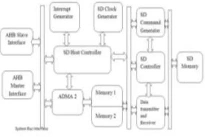
The SD Host Controller is fully compliant to SD Host Controller Specification version 3.0 and Physical Layer
Specification version 3.01. The standard register set is implemented. The Host Processor accesses the various
registers and FIFOs in the Host Controller to transfer data between Host and SD Card.
Fig 1.1: Basic block diagram of SDHC
Every data transfer is preceded by corresponding command and response. Command is send by the Host
Controller to the Card and Response is send back by the Card to the Host Controller. The block diagram of Host
Controller is given in Figure 1.1
2.2 Data Transfer Modes
The SD Host Controller supports three modes to transfer Data between System and the card. The three modes
include Non-DMA, DMA and ADMA mode. In Non-DMA mode (also known as "programmed I/O" method)
the Host Controller has a data buffer for data transfer. The Host Driver accesses internal buffer through the
1172 |
P a g e
pointer is not directly accessible by the Host Driver. Every time the Buffer Data Port register is accessed, the
pointer is incremented depending on amount of data written.
In DMA mode, the data transfer between system memory and SD card takes place without interruption of CPU
execution. DMA shall support both single block and multiple-block transfers but does not support infinite
transfers. The result of a DMA transfer shall be the same regardless of the system bus data transfer method.
DMA had disadvantage that DMA Interrupt generated at every page boundary disturbs CPU to reprogram the
new system address.
This DMA algorithm forms a performance bottleneck by interruption at every page boundary.
A new DMA transfer algorithm called ADMA (Advanced DMA) is defined that adopts scatter gather DMA
algorithm so that higher data transfer speed is available. The Host Driver can program a list of data transfers
between system memory and SD card to the Descriptor Table before executing ADMA. It enables ADMA to
operate without interrupting the Host Driver. Furthermore, ADMA can support not only 32-bit system memory
addressing but also 64-bit system memory addressing.
The 32-bit system memory addressing uses lower 32-bit field of 64-bit address registers. ADMA adopts scatter
gather DMA algorithm so that higher data transfer speed is available. The Host Driver can program a list of data
transfers between system memory and SD card to the Descriptor Table before executing ADMA. It enables
ADMA to operate without interrupting the Host Driver. Furthermore, ADMA can support not only 32-bit
system memory addressing but also 64-bit system memory addressing. The 32-bit system memory addressing
uses lower 32-bit field of 64-bit address registers.
2.3 Direct Memory Access (DMA)
DMA is an essential feature of all modern computers, as it allows devices to transfer data without subjecting the
CPU to a heavy overhead. Otherwise, the CPU would have to copy each piece of data from the source to the
destination. This is typically slower than copying normal blocks of memory since access to I/O devices over a
peripheral bus is generally slower than normal system RAM. During this time the CPU would be unavailable for
any other tasks involving CPU bus access, although it could continue doing any work which did not require bus
access. A DMA transfer essentially copies a block of memory from one device to another. While the CPU
initiates the transfer, it does not execute it. For so-called "third party" DMA, as is normally used with the ISA
bus, the transfer is performed by a DMA controller which is typically part of the motherboard chipset. More
advanced bus designs such as PCI typically use bus mastering DMA, where the device takes control of the bus
and performs the transfer itself. A typical usage of DMA is copying a block of memory from system RAM to or
from a buffer on the device.
Such an operation does not stall the processor, which as a result can be scheduled to perform other tasks. DMA
is essential to high performance embedded systems. It is also essential in providing so-called zero-copy
implementations of peripheral device drivers as well as functionalities such as network packet routing, audio
1173 |
P a g e
III. DRAWBACKS OF DMA
A typical usage of a DMA is to transfer a block of memory from/to an external memory or from/to a buffer on
the device. A DMA is usually used in high performance embedded systems. The alignment process subjects the
CPU to a heavy overhead. There are some applications, like video processing that require an efficient support
for unaligned accesses, degrading the performance significantly.
IV. SDMA, ADMA 1 DISADVANTAGES
Single operation DMA (SDMA) interrupts the host CPU at every page boundary while the ADMA reduces the
load on the host CPU. It supports both 32-bit and 64-bit system memory addressing. ADMA2 improves upon
ADMA1 by removing restrictions on data location and size. DMA shall only support both single block and
multiple-block transfers but does not support infinite transfers.
DMA had disadvantage that DMA Interrupt generated at every page boundary disturbs CPU to reprogram the
new system.This SDMA algorithm forms a performance bottleneck by interruption at every page boundary. A
new DMA transfer algorithm called ADMA2 (Advanced DMA 2) provides higher data transfer speed. DMA
allows an I/O device to communicate directly to the main memory bypassing CPU (Central Processing Unit) in
order to speed up memory operations. When used with DMA the CPU initiates the transfer, does other
operations while the transfer is in progress, and receives an interrupt from the DMA controller when the
operation is done. Computers that have DMA channels can transfer data to and from devices with much less
CPU overhead than computers without a DMA channel.
V. ADVANCED DIRECT MEMORY ACCESS 2 (ADMA 2)
ADMA 2 is one of several methods for coordinating the timing of data transfers between an input/output (I/O)
device and the core processing unit or memory in a computer. ADMA 2 is one of the faster types of
synchronization mechanisms, generally providing significant improvement over interrupts, in terms of both
latency and throughput.
5.1 Principle of ADMA 2
ADMA 2 controller can generate memory addresses and initiate memory read or write cycles. It contains
several processor registers that can be written and read by the CPU. These include a memory address register, a
byte count register, and one or more control registers The CPU then sends commands to a peripheral device to
initiate transfer of data. The ADMA 2 controller then provides addresses and read/write control lines to the
system memory. Each time a byte of data is ready to be transferred between the peripheral device and memory,
the ADMA 2 controller increments its internal address register until the full block of data is transferred.
The figure 5.1 shows the block diagram of advanced ADMA2.In ADMA2 operation a Descriptor Table is
created in system memory by the Host Driver. bit Address Descriptor Table is used for the system with
1174 |
P a g e
Fig 5.1: Block diagram of ADMA 2
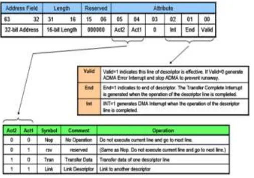
Each descriptor line (one executable unit) consists with address, length and attribute field. The attribute
specifies operation of the descriptor line. ADMA2 includes SDMA, State Machine and Registers circuits.
ADMA2 does not use 32-bit SDMA System Address Register but uses the 64-bit Advanced DMA System
Address register for descriptor pointer. Writing Command register triggers off ADMA2 transfer. ADMA2
fetches one descriptor line and executes it. This procedure is repeated until end of descriptor is found.
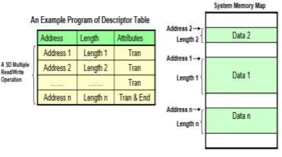
5.2 An Example of ADMA2 Programming
Fig 5.2: An Example of ADMA2 Data Transfer
Figure 5.2 shows a typical ADMA2 descriptor program. The data area is sliced in various lengths and each slice
is placed somewhere in system memory. The Host Driver describes the Descriptor Table with set of address,
length and attributes. Each sliced data is transferred in turns as programmed in descriptor.
5.3 Block Count Register
Block count register is enabled when Block Count Enable in the Transfer Mode register is set to 1.The Host
Controller decrements the block count after each block transfer and stops when the count reaches zero. Setting
the block count to 0 results in no data blocks is transferred. This register should be accessed only when no
1175 |
P a g e
write operations are ignored. When a suspend command is completed, the number of blocks yet to be transferred
can be determined by reading this register.
5.4 Data Address and Data Length Requirements
There are 3 requirements to program descriptor.
The maximum data length of each descriptor line is less than 64KB.
Total Length = Length 1 + Length 2 + …Length n Total length = multiple of Block Size
If total length of a descriptor were not multiple of block size, ADMA2 transfer should be aborted by data
timeout.
5.5 Descriptor Table
Fig 5.3: Example of Descriptor table
Figure 5.3 shows the definition of 32-bit Address Descriptor Table. One descriptor line consumes 64-bit
(8-byte) memory space. Attribute is used to control descriptor. 3 action symbols are specified. "Nop" operation
skips current descriptor line and fetches next one. "Tran" operation transfers data designated by address and
length field. "Link" operation is used to connect separated two descriptors. The address field of link points to
next Descriptor Table. The combination of Act2=0 and Act1=1 is reserved and defined the same operation as
Nop.
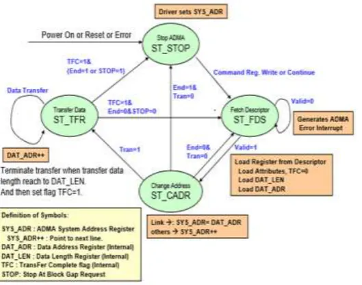
5.6 ADMA2 States and its Operation
The figure shows various states of ADMA2 and the operation of all states. It also describes the condition when
ADMA 2 fetches the descriptor line and transfer the data and the increment in the address. ADMA 2 adopts
scatter gather DMA algorithm so that higher data transfer speed.
The Host Driver can program a list of data transfers between system memory and SD card to the Descriptor
Table before executing ADMA. It enables ADMA to operate without interrupting the Host Driver. Furthermore,
ADMA can support not only 32-bit system memory addressing but also 64-bit system memory addressing. The
1176 |
P a g e
ST_FDS (Fetch Descriptor): ADMA 2 fetches a descriptor line and set parameters in internal registers. Nextgo to ST_CADR state.
Fig 5.6: States of ADMA 2
ST_CADR (Change Address): Link operation loads another Descriptor address to ADMA 2 System Address
register. In other operations, ADMA System Address register is incremented to point next descriptor line. If
End=0, go to ST_TFR state. ADMA 2 shall not be stopped at this state even if some errors occur.
ST_TFR(Transfer Data ): Data transfer of one descriptor line is executed between system memory and SD
card. If data transfer continues (End=0) go to ST_FDS state.
ST_STOP (Stop DMA): After Power on reset or software reset. All descriptor data transfers are completed.
Error occurrence during ADMA2 transfer may stops ADMA2 operation and generates ADMA 2 Error Interrupt.
Error Status register holds state of ADMA 2 stopped. The host driver can identify error descriptor location by
following method. If ADMA 2 stopped at ST_FDS state, the ADMA 2 System Address Register points the error
descriptor line. If ADMA 2 stopped at ST_TFR or ST_STOP state, the ADMA 2 System Address Register
points the next location of error descriptor line. By this reason, ADMA2 shall not stop at ST_CADR state.
ADMA 2 allows an I/O device to communicate directly to the main memory bypassing CPU in order to speed
up memory operations. When the CPU is using programmed input/output (I/O) without DMA, it is fully
occupied for the entire duration of the read/write operation, and is thus unavailable to perform other work. When
used with ADMA, the CPU initiates the transfer, does other operations while the transfer is in progress, and
receives an interrupt from the ADMA controller ( a special purpose processor used to transfer data between
memory and I/O devices) when the operation is done.
1177 |
P a g e
Fig 6.1: Reset function for command line 00
In fig 6.1 data is received from memory card, it is said to be in wait mode. Data will either be read or write in
host depending on command line.
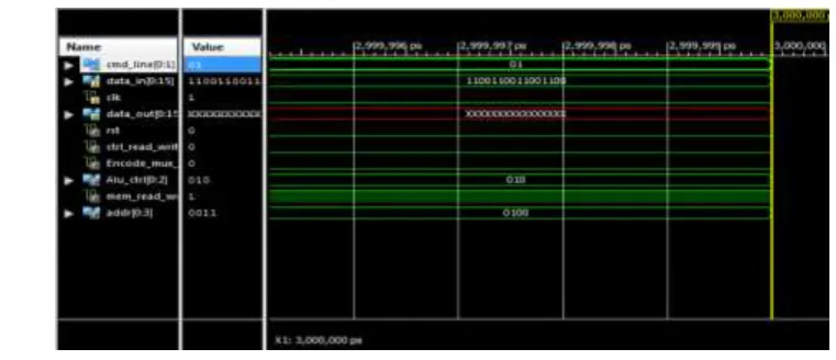
Fig 6.2: Read function for command line 01
In fig 6.2 data is received from memory card. It is said to perform read function as command line is changed
from 00 to 01. The data is read from memory card
1178 |
P a g e
In figure 6.3 read operation is completed. It is said to perform write operation as the command line is changed
from 01 to 10.
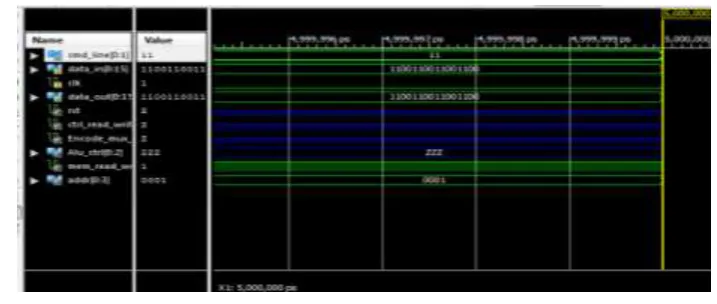
Fig 6.4: Undefined state for command line 11
Undefined function or high impedance as command line is 11.
VII. CONCLUSION
The battery operated device which is one of the fastest growing electronic industries, in which speed of data
transfer is becoming a major issue. With the proposed design of secure digital host controller intellectual
property, we can achieve a high speed data transfer without compromising power. Simulated results for data
transfer in ADMA 2 which provides high capacity data transfer with the reduction in load on Host CPU is
obtained.
7.1 Further Enhancement
In coming years SD technology will be the de-facto industry standard for mobile phones, digital cameras and
other portable multimedia entertainment devices. Future plan is to do the functional verification of Designed
ADMA 2 and to work on next generation SD which is SDXC (extended Capacity) memory card specification.
In this technology the storage capacity of the SD card will be from 32 GB to 2 TB.
REFERENCES
1. Technical Committee SD Association. (2011): SD Specifications Part A2 SD Host Controller Simplified.
2. Specification Version 3.00. Retrieved February 25, 2011 from SD ..
3. Technical SD association: SD Specifications Physical Layer Simplified SpecificationVersion 3.01.
Retrieved February 18, 2011 from SD card.
4. AMBA Advanced High Performance Bus Protocol specification http://www.arm.com.
5. Chuan-Sheng Lin and Lan-Rong Dung, “A NAND Flash Memory Controller for SD/MMC Flash Memory
Card”. IEEE Transactions on Magnetics, vol.43, No.2, February2007.
6. P. Rashinkar, P. Paterson, Leena singh, “System-on-a-chip verification methodology and techniques,”
Kluwer Academic Publishers, 2001.
7. SD Association: SD Memory Card Choices.