University of Pennsylvania
ScholarlyCommons
Publicly Accessible Penn Dissertations
Spring 5-17-2010
Multiscale Modeling and Simulations of Defect
Clusters in Crystalline Silicon
Sumeet S. Kapur
University of Pennsylvania, [email protected]
Follow this and additional works at:http://repository.upenn.edu/edissertations
Part of theOther Chemical Engineering Commons, and theThermodynamics Commons
Recommended Citation
Kapur, Sumeet S., "Multiscale Modeling and Simulations of Defect Clusters in Crystalline Silicon" (2010).Publicly Accessible Penn Dissertations. 109.
Multiscale Modeling and Simulations of Defect Clusters in Crystalline
Silicon
Abstract
As the device dimension in semiconductor silicon transistors reach sub-20nm, it significantly enhances the tolerance limits on the size and concentration of defects in the underlying crystalline silicon wafer.
Understanding the evolution of defect clusters is critical for controlling the defect density and size distribution within crystalline silicon. The objective of this thesis is to develop the computational
methodology that quantitatively describes the evolution of defect clusters in crystalline solids at an atomistic level, and provide a mechanistic understanding of underlying physics behind the defect aggregation process.
In first part of the thesis we develop a novel computational method for probing the thermodynamics of defects in solids. We use this to estimate the configurational entropy of vacancy clusters which is shown to substantially alter the thermodynamic properties of vacancy clusters in crystals at high temperature. The modified thermodynamic properties of vacancy clusters at high temperature are found to explain a longstanding discrepancy between simulation predictions and experimental measurements of vacancy aggregation dynamics in silicon.
In the next part, a comprehensive atomistic study of self-interstitial aggregation in crystalline silicon is presented. The effects of temperature and pressure on the aggregation process are studied in detail and found to generate a variety of qualitatively different interstitial cluster morphologies and growth behavior. A detailed thermodynamic analysis of various cluster configurations shows that both vibrational and configurational entropies are potentially important in setting the properties of small silicon interstitial clusters. The results suggest that a competition between formation energy and entropy of small clusters could be linked to the selection process between various self-interstitial precipitate morphologies observed in ion-implanted crystalline silicon.
Finally in the last section, we investigate the effect of carbon on self-interstitial aggregation. The presence of carbon in the silicon dramatically reduces cluster coalescence, with almost no direct effect on the single self-interstitials. This suggests that suppression of transient enhanced diffusion of boron (in presence of carbon), could be due to the direct interaction between carbon atoms and self-interstitial clusters.
Degree Type Dissertation
Degree Name
Doctor of Philosophy (PhD)
Graduate Group
Chemical and Biomolecular Engineering
Keywords
Silicon, Defects, Inerstitials, Vaccancies, Stress
Subject Categories
MULTISCALE MODELING AND SIMULATIONS
OF DEFECT CLUSTERS IN CRYSTALLINE
SILICON
Sumeet S. Kapur
A DISSERTATION
in
Chemical and Biomolecular Engineering
Presented to the Faculties of the University of Pennsylvania
in
Partial Fulfillment of the Requirements for the
Degree of Doctor of Philosophy
2010
Dr. Talid R. Sinno, Supervisor of Dissertation
Dr. Matthew J. Lazzara, Graduate Group Chairperson
Acknowledgements
I would like to express my deepest appreciation to my advisor, Professor Talid R. Sinno,
for his guidance and invaluable support throughout my graduate career at the University
of Pennsylvania. It has been the most enjoyable and satisfying experience to work with a
person of his caliber and enthusiasm. His willingness in having regular, insightful
discussions and his quest for achieving the most accurate results provided me with the
inspiration to work with immense interest and dedication. I also wish to thank the other
members of my committee, Professor John L. Bassani, Professor Scott L. Diamond and
Professor John C. Crocker, for their patient direction and helpful criticism.
I am very grateful to my officemates and colleagues Manish Prasad, Tom Frewen,
Jainguo Dai, Raynaldo Scarlett, and Alex Nieves who have contributed immensely to my
personal and professional time at Penn. The group has been a source of friendships as
well as good inputs and collaboration. I am also grateful to our Graduate Assistant,
Marge Addario and Office Manager, John Linscheid, who kept us organized and were
always ready to help.
Finally, I would like to extend a heartfelt thank you and love to my parents Jaswant Kaur
and Pritpal Singh Kapur, my sister Harpreet, and my wife Ritu for their constant love and
ABSTRACT
MULTISCALE MODELING AND SIMULATIONS OF DEFECT
CLUSTERS IN CRYSTALLINE SILICON
Sumeet S. Kapur
Supervisor: Professor Talid R. Sinno
As the device dimension in semiconductor silicon transistors reach sub-20nm, it
significantly enhances the tolerance limits on the size and concentration of defects in the
underlying crystalline silicon wafer. Understanding the evolution of defect clusters is
critical for controlling the defect density and size distribution within crystalline silicon.
The objective of this thesis is to develop the computational methodology that
quantitatively describes the evolution of defect clusters in crystalline solids at an
atomistic level, and provide a mechanistic understanding of underlying physics behind
the defect aggregation process.
In first part of the thesis we develop a novel computational method for probing
the thermodynamics of defects in solids. We use this to estimate the configurational
entropy of vacancy clusters which is shown to substantially alter the thermodynamic
properties of vacancy clusters in crystals at high temperature. The modified
thermodynamic properties of vacancy clusters at high temperature are found to explain a
longstanding discrepancy between simulation predictions and experimental
In the next part, a comprehensive atomistic study of self-interstitial aggregation in
crystalline silicon is presented. The effects of temperature and pressure on the
aggregation process are studied in detail and found to generate a variety of qualitatively
different interstitial cluster morphologies and growth behavior. A detailed
thermodynamic analysis of various cluster configurations shows that both vibrational and
configurational entropies are potentially important in setting the properties of small
silicon interstitial clusters. The results suggest that a competition between formation
energy and entropy of small clusters could be linked to the selection process between
various self-interstitial precipitate morphologies observed in ion-implanted crystalline
silicon.
Finally in the last section, we investigate the effect of carbon on self-interstitial
aggregation. The presence of carbon in the silicon dramatically reduces cluster
coalescence, with almost no direct effect on the single self-interstitials. This suggests that
suppression of transient enhanced diffusion of boron (in presence of carbon), could be
Table of Contents
Acknowledgements ... ii
ABSTRACT ... iii
Table of Contents ... v
List of Tables ... x
List of Figures ... xi
1 Introduction and Motivation ... 1
1.3.1 Effect of Impurities (Carbon) on Self-Interstitial Clustering in Silicon. ... 15
2 Thermodynamic and Structural Properties of Vacancy Clusters ... 23
2.2.1 Configurational Entropy ... 28
1.1 Defects in Crystalline Semiconductor Silicon ... 4
1.2 Void Formation during Czochralski Crystal Growth ... 7
1.3 Interstitial Aggregation during post Ion-Implant Annealing ... 10
1.4 Overall Computational Framework ... 18
1.5 Thesis Objective and Outline ... 21
2.1 Thermodynamics of Cluster Aggregation Process ... 24
2.4.1 Wang-Landau Monte Carlo (WLMC) Method ... 36
2.4.2 Validation of WLMC Approach ... 38
2.4.3 Dependence of Density of States on Interaction Distance ... 42
2.4.4 Probability Distribution Functions for On-Lattice Vacancy Clusters… ... 43
2.5.1 Absolute Probability Distribution and Density of States Functions 49 2.5.2 Total Cluster Free Energy Calculations ... 55
2.5.3 Connections to Experimental Data ... 60
2.5.4 Explicit Configurational Entropy Calculations ... 61
2.5.5 Effect of Off-Lattice States on Single Vacancy ... 66
2.5.6 Comparison to Tersoff Empirical Potential ... 68
2.6.1 Cluster Morphological Estimation ... 70
3 Atomistic Simulations of Self-Interstitial Aggregation ... 77
2.3 Cluster Formation Thermodynamics from Potential Energy Landscape .... 31
2.4 On-Lattice Calculations of Cluster Free Energy ... 35
2.5 Off-Lattice Calculations of Cluster Free Energy ... 45
2.6 Cluster Capture Radius ... 69
3.3.1 Effect of Hydrostatic Pressure on the Aggregation Behavior of
Self-Interstitials ... 97
3.3.2 Kinetic Considerations for the 3D-2D Morphological Transformation ... 102
3.4.1 Tersoff Potential Simulations ... 104
3.4.2 Stillinger-Weber Potential Simulations ... 108
4 Thermodynamics Analysis of Self-Interstitial Clusters ... 113
4.1.1 Formation Energy Calculations for Self-Interstitial Clusters – Ground State Configurations ... 117
4.1.2 Formation Free Energy Calculations for Self-Interstitial Clusters – Ground State Configurations ... 119
3.1 A Brief Overview of Observed Self-Interstitial Cluster Morphologies in Silicon… ... 79
3.2 Simulation Methodology for Large-Scale Simulations of Interstitial Aggregation ... 89
3.3 Direct MD Simulation of Self-Interstitial Aggregation – EDIP Results ... 91
3.4 Direct MD Simulation of Self-Interstitial Aggregation – Other Potentials….. ... 104
3.5 Conclusions ... 109
4.3.1 Probability Distribution Functions for Small Clusters at Zero
Pressure ... 128
4.3.2 The Effect of Hydrostatic Lattice Strain on the Thermodynamics of Small Interstitial Clusters ... 134
4.6.1 Low temperature and/or tensile lattice strain ... 150
4.6.2 Higher temperatures with no compression ... 151
5 Carbon Mediated Self-Interstitial Clustering in Silicon ... 155
5.1.1 Simulation conditions ... 158
5.1.2 Validity of the Tersoff multi-component empirical potential ... 159
5.2.1 Identification of interstitial clusters ... 160
4.2 Computational Framework for Single Cluster Thermodynamic Analysis 125 4.3 Thermodynamic Analysis of Single Self-Interstitial Clusters – EDIP Results.. ... 128
4.4 Calculation of Formation Enthalpy PDFs ... 142
4.5 Tersoff Potential Results ... 148
4.6 A Mechanistic Summary and Conclusions ... 150
5.1 Large Scale Parallel MD Simulation of Carbon and Silicon Self-Interstitial Aggregation ... 157
5.2.2 Structure of interstitial clusters ... 162
5.3.1 Size Distribution Evolution ... 169
5.3.2 A. Mean-field scaling approximation for aggregation ... 172
5.3.3 Capture radius model for interstitial clusters and scaling predictions.. ... 174
5.3.4 Atomistic Studies of Cluster Diffusion ... 175
5.4.1 Sensitivity to Empirical Potential Model ... 181
5.4.2 Sensitivity to Defective Atom Identification ... 183
6 Conclusions ... 194
6.1.1 Effect of Non-Hydrostatic (Biaxial and Uniaxial Stress) on defect clustering ... 199
6.1.2 Cluster Patterning in Multi-Component Systems ... 200
Bibliography ... 203
5.3 Mean Field Scaling Analysis ... 169
5.4 Sensitivity Analysis ... 181
5.5 Continuum Rate Equation Modeling ... 187
5.6 Conclusions ... 193
List of Tables
Table 1.1: Examples of Crystalline Defects [54] ... 5 Table 2.1: Power law coefficients aand bas a function of temperature for average
vibrational entropy contribution to the total free energy ... 64 Table 5.1: System size and interstitial cluster size used for cluster diffusivity
measurements as a function of carbon concentration (%C). ... 177
Table 5.2: Power law exponent, p, for cluster diffusivity (Dneff(%C)~np) as a function
List of Figures
Figure 1.1: Schematic description of the Integrate Circuit (right image) – heart of all electronic devices. [1, 2] ... 1 Figure 1.2: Moore’s Law (dotted curve) predicts doubling transistor count every two
years, Solid point/line: actual Data from Intel Processors, closely following Moore’s law for almost 3 decades. [5] ... 3 Figure 1.3: Feature length Time Line from Intel [5]. Numbers on curve indicate the
transistor gate oxide thickness in nm. ... 4 Figure 1.4: Examples of Defects in Crystalline Lattice (a) Impurity Interstitial (b)
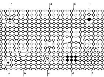
Dislocation Line (c) Self-Interstitial (d) Cluster of Impurity Atoms (e) Extrinsic Dislocation Loop (f) Small Substitutional Impurity (g) Vacancy (h) Intrinsic Dislocation Loop (i) Large Substitutional Impurity. [54] ... 6 Figure 1.5: Schematic Representation of Czochralski Crystal Growth Process, (a)
Czochralski Furnish (b) poly-crystalline silicon in quartz crucible (c) single-crystal seed is dipped into the molten poly-crystalline silicon (d,e) single-crystal silicon is grown by rotating and pulling the seed up. [4] ... 8 Figure 1.6: TEM Images of an octahedral void. [154] ... 10 Figure 1.7: Schematic representation of ion implantation and annealing process in silicon wafers. Dopant(B) implantation on a given area is carried out to achieve the desired electronic characteristics. Implantation damages the underlying silicon lattice, which is treated by annealing. Annealing leads to spreading of dopant profiles as these diffuse outwards. [123] ... 11 Figure 1.8: Boron concentration profile spreads outwards post implantation anneal at
800oC.[109] ... 13 Figure 1.9: HRTEM image of {113} defect in (a), enlarged picture of marked line in (a)
Figure 1.10: Different types of extended interstitial defects after post implant annealing.[28] ... 15 Figure 1.11: Impact of carbon on boron diffusion: (a) Boron concentration profile spreads out post Si implantation anneal for a background carbon concentration of 10 /18 cm3, (b) No spreading in boron concentration profile is observed when the carbon concentration is increased to2 10 /x 19 cm3. [141] ... 17 Figure 2.1: Hexagonal ring clusters (HRC) containing (a) 6, (b) 10, and (c) 14 vacancies.
... 27 Figure 2.2: (a) Centres of mass of several dimmers on a two dimensional lattice (left). (b) Full center-of-mass lattice for dimmers is twice as dense as that of actual lattice (right). ... 29 Figure 2.3: (a) Centers of mass of 1NN and 2NN dimers on a two-dimensional lattice
(left). (b) Full center-of-mass lattice for 1NN and 2NN dimmers (right). ... 30 Figure 2.4: DOS for a 1st-nearest neighbor connected 6-vacancy cluster calculated using (a) WLMC (diamonds) and (b) direct counting (circles). Also shown are the results from a corrected-bias WLMC (squares). ... 39 Figure 2.5: Network connectivity and transition probabilities for an energetically
degenerate four-state system – (a) Uniformly connected, (b) Non-uniformly connected. ... 40 Figure 2.6: DOS for 6V cluster as a function of vacancy-vacancy interaction distance.
Lower Dash – 2NN, Thin Solid – 3NN, Upper Dash – 6NN, Thick Solid – 8NN. .. 43 Figure 2.7: Probability distribution functions for the 6V cluster at (a) 1600K (squares),
Figure 2.10: Probability distribution functions for vacancy clusters at 1600 K obtained directly from MD. ... 50 Figure 2.11: Overlap between probability distributions sampled at two different
temperatures for the 6V and 18V clusters. Solid symbols – low T, Open symbols – high T. All data shown is scaled to the lower temperature (1400K for 6V, 1050K for 18V). ... 52 Figure 2.12: Absolute density-of-states functions. Small squares – data derived from
sampling at 1600K; Solid circles – directly counted HRC degeneracy; Large open circles – DOS sampled at 1400K (6V) and 1050K (18V); solid lines – exponential fits. ... 53 Figure 2.13: DOS exponent dependence on cluster size. Line is a power-law fit. ... 54 Figure 2.14: Temperature and size dependence of the total effective surface free energy (σ ) of vacancy clusters predicted using the EDIP potential. Lower surface: current results including configurational entropy, Upper surface: HRC calculations with vibrational entropy only. ... 56 Figure 2.15: Difference ratio, (σHRC −σFULL)/σFULL, between current (σFULL) and HRC
(σHRC) surface free energy calculations. ... 59
Figure 2.16: Vibrational Entropy as a function of formation energy of various configurations for 10V (circles), 18V (squares) clusters. Lines represent the linear fit to the data. ... 62 Figure 2.17: Configurational entropy contribution to the free energy of formation as a
function of temperature for various cluster sizes. Dash line – limiting behavior for (111) surface melting. ... 65 Figure 2.18: DOS (circles) and PDF at 1600K (squares) for the single vacancy. ... 66 Figure 2.19: Probability distribution function for the 10V cluster. (a) Solid squares –
Figure 2.20: (a) Effective Cluster capture radius as a function of number of vacancies for various displacement threshold values: β=0.178Å (diamonds), β=0.136Å
(squares), and β=0.08Å (circles). ... 72
Figure 2.21: Temperature dependence of the cluster capture radius for β=0.136Å :
T=1600K (squares) and T=1300K (circles). Solid line represents the capture radius assuming compact spherical morphology (eq. ((2.21)). ... 73 Figure 2.22: Morphological evolution of vacancy clusters as a function of size for
temperatures below the surface melting point. ... 74 Figure 3.1: HRTEM image of interstitial aggregates created in silicon during in
situ-electron irradiation at room temperature. The {113} and {111} defect are marked with single and double arrow [50]. ... 80 Figure 3.2: HRTEM image of {113} defect in (a), enlarged picture of marked line in (a) is shown in (b). The small open and solid circles represent the interstitials, separated by large open circles (8 membered rings) [34] ... 81 Figure 3.3: A HRTEM observation of single LID (a) HRTEM Image (b) atomic
simulated image (c) atomic model superimposed on the HRTEM image. The middle arrowheads represent single LID. Also shown in (c) are two double-LID (two side-by-side single LID)[46] ... 82 Figure 3.4: Schematic representation of various configurations of {113} based on
different arrangements of /I/ and /0/ repeat units. (a): shows /I/ structure where the I chain occurs repeatedly, (b): shows /IO/ structure, where the every I chain is separated by an empty ‘O’ chain.; (c) /IIO/ structure where ‘O’ chain separates a pair of ‘I’ chains. Asterisks or eight membered rings represent ‘O’ chains in above figure. [48] ... 83 Figure 3.5: TEM of Frank Dislocation Loop (left), and Perfect Dislocation Loop (right) 84 Figure 3.6: HRTEM image of {111}-defect after (a) 30, (b) 35 min irradiation (c)
HRTEM superimposed atomic image based on rectangle in (b). [33] ... 85 Figure 3.7: A {100} defect based on Humble/Arai 4I structure [52]. ... 86 Figure 3.8: HRTEM image of {100} loop under high Boron implant. Vertical Axis is
Figure 3.9: (a)-(c) System-wide evolution of interstitial cluster distribution at 1200K and zero pressure; (a) t=0.2ns, (b) t=3.7 ns, and (c) t=19.2 ns. Large (red) spheres denote self-interstitials; small (green) spheres show lattice atoms that are displaced by more than 0.2Å from their equilibrium positions. All other atoms are deleted for clarity. (d)-(g) Detailed view of cluster structures; (d) {111} RLD, (e) {111} PDL, (f) {111} FDL, and (g) {100} planar defect. All panels are oriented so that the horizontal direction is [110]. For figures (a)-(c) and (g), vertical direction is [001], for figures (d)-(e) vertical direction is [111]. ... 92 Figure 3.10: System-wide evolution of interstitial cluster distribution at 1300K and zero pressure. Total simulation time is 13.4 ns. Large (red) spheres denote self-interstitials; small (green) spheres show lattice atoms that are displaced by more than 0.2Å from their equilibrium positions. All other atoms are deleted for clarity. Horizontal direction is [110] and vertical [001]. ... 94 Figure 3.11 : System-wide evolution of interstitial cluster distribution at 1400K and zero pressure. Total simulation time is 8.0 ns. Large (red) spheres denote self-interstitials, small (green) spheres show lattice atoms that are displaced by more than 0.2Å from their equilibrium positions. All other atoms are deleted for clarity. Horizontal direction is [110] and vertical [001]. ... 94 Figure 3.12: Average number of interstitials in clusters transitioning from
three-dimensional to two-three-dimensional morphology as a function of temperature (zero pressure). ... 95 Figure 3.13: System-wide evolution of interstitial cluster distribution at 1200K and 3GPa pressure (approx. 1% compressive strain). Total simulation time is 9.6 ns. Large (red) spheres denote self-interstitials; small (green) spheres show lattice atoms that are displaced by more than 0.2Å from their equilibrium positions. All other atoms are deleted for clarity. Horizontal direction is [100] and vertical is [001]. ... 98 Figure 3.14: (a)-(c) (a)-(c) System-wide evolution of interstitial cluster distribution at
deleted for clarity. (d)-(g) Detailed view of individual cluster structures; (d) 4-intersitial Humble/Arai configuration, (e) partially reconstructed LID, a precursor to {113} defects, (f) {113} planar defect comprised of three <110>-oriented interstitial chains (shown), and (g) two Humble/Arai 4-interstitial clusters arranged to form a {100} planar defect. All panels except (f) are oriented so that the horizontal
direction is [110] and vertical is [001]. In (f), vertical is [113], horizontal is [332]. ... 99 Figure 3.15: System-wide evolution of interstitial cluster distribution at 1400K and -3GPa pressure (approx. 1% tensile strain). Total simulation time is 7.4 ns. Large (red) spheres denote self-interstitials; small (green) spheres show lattice atoms that are displaced by more than 0.2Å from their equilibrium positions. All other atoms are deleted for clarity. Horizontal direction is [100] and vertical is [001]. ... 102 Figure 3.16: Evolution of self-interstitial clusters during strain relaxation at 1200K.(a)
After 10 ns at +3 GPa, (b) 0.3 ns later as the pressure was reduced from +3 GPa to 0, and (c) after a further 6.9 ns at zero pressure. Large (red) spheres denote self-interstitials; small (green) spheres show lattice atoms that are displaced by more than 0.2Å from their equilibrium positions. All other atoms are deleted for clarity. Arrows denote onset of 3d-2d transition following pressure drop to zero. For all frames, horizontal direction is [100] and vertical is [001]. ... 103 Figure 3.17: System-wide evolution of interstitial cluster distribution at zero pressure and (a) 1900K, (b) 2100K, and (c) 2250K using the Tersoff potential. Large (red) spheres denote self-interstitials; small (green) spheres show lattice atoms that are displaced by more than 0.2Å from their equilibrium positions. All other atoms are deleted for clarity. Horizontal direction is [110] and vertical is [001]. ... 106 Figure 3.18: Tersoff simulation at 1900 K and +3GPa after 6.1 ns of simulation; no
Figure 3.19: Stillinger-Weber simulations at: (a) 1330 K and zero pressure at 3.3 ns, (b) 1500 K and zero pressure at 2.8 ns, and (c) 1500 K and -3GPa at 1.9 ns. Horizontal direction is [110] and vertical is [001]. ... 109 Figure 4.1: Formation energies (Ef) per interstitial as a function of cluster size (nI).
Squares: EDIP results for the structures corresponding to those identified in refs. [96] and [104].; for nI ≥6, formation energies for both compact (open squares) and
elongated (filled squares) are shown (see text for definitions). Circles: DFT results from ref. [104]. Diamonds: DFT results from ref. [96]. ... 118 Figure 4.2: EDIP formation free energies (Gf) as a function of interstitial cluster size at
1100 K. Open squares: compact structures. Filled squares (nI ≥6): elongated
structures. Diamond symbol shows free energy including the estimated configurational entropy (see text). Inset: QHA-EDIP formation vibrational entropies as a function of cluster size at 1100 K. Open circles: compact structures. Filled circles: elongated structures. ... 120 Figure 4.3: Nearly degenerate configurations for the compact eight-interstitial cluster
based on combinations of two Humble/Arai four-interstitial building blocks. Left-hand panels are projections normal to [100], right-Left-hand panels are projections normal to [110]: (a) Ef =16.23 eV, (b) Ef =15.95 eV, and (c) Ef =15.86 eV. ... 122 Figure 4.4: (a) Formation energy PDFs (at 1100 K), and (b) DOS for small interstitial
clusters in the size range 3≤nI ≤8 computed with the EDIP potential. For both
panels, squares representnI =3, circlesnI =4, gradientsnI =5, deltasnI =6,
diamondsnI =7, and left trianglesnI =8. Insets in (a) show two configurations for
the 4-interstitial cluster; upper – Humble/Arai configuration, lower – extended, higher energy configuration. ... 129 Figure 4.5: Vibrational entropy of formation for (a) 6-vacancy, (b) 10-vacancy, (c)
Figure 4.6: 4-interstitial cluster PDFs as a function of temperature. Squares – 1100K, circles – 1200K, diamonds – 1300K. ... 134 Figure 4.7: (a) PDF for the 4-interstitial cluster as a function of hydrostatic pressure
(lattice strain): squares – zero stress; circles – -3GPa applied pressure (1% tension); diamonds – +3GPa applied pressure (1% compression). Inset: formation thermodynamics for the 4-interstitial Humble/Arai configuration as a function of strain (diamonds – free energy, circles – energy, squares – vibrational entropy). (b) 4-interstitial DOS as a function of hydrostatic pressure (lattice strain) anchored to the Humble/Arai configuration (see text): squares – zero strain; circles – 1% tension; diamonds – 1% compression. ... 135 Figure 4.8: Effect of isotropic tensile strain on the probability distribution functions for the 5-, 8-, and 12-interstitial clusters (shown left to right, respectively). Filled squares denote zero strain, open circles denote 1% tensile strain (-3GPa applied pressure). ... 138 Figure 4.9: Formation energy PDF for the 8-interstitial cluster at 1100K and -3GPa
applied pressure (1% tensile strain) highlighting the distribution at low values of formation energy. The 8-interstitial configurations that correspond to the various numbered locations on the PDF are shown in the insets on the right-hand side of the figure. ... 139 Figure 4.10: Formation energy PDF for the 4-interstitial cluster at 1100K and zero
Figure 4.13: Formation volume as a function of formation energy for 4-interstitial configurations at zero pressure. ... 147 Figure 4.14: Tersoff generated (NVT MD) formation energy PDFs for the 4-interstitial
(left) and 8-interstitial (right) clusters at 1900K as a function of applied strain: open circles – zero pressure, small filled squares – +3GPa applied pressure (approx. 1% compressive strain). ... 149 Figure 4.15: Evolution map for self-interstitial aggregation as a function of cluster size and temperature. In most cases, the effect of hydrostatic pressure is qualitatively similar to increasing the temperature. ... 153 Figure 5.1: Distribution of Defective Atoms (DAs) at t=3.46ns. (a) pure Si (4337 DAs),
and (b) 0.9% C-doped Si (3164 DAs). Note that the number of DAs is much greater than the number of interstitials (1000) because of lattice strain effects. ... 164 Figure 5.2: Defective atom distribution in pure Silicon at 3.46 ns ... 165 Figure 5.3: Defective Atom Distribution in 0.9% C-doped Silicon at 3.46 ns ... 166 Figure 5.4: Aspect Ratio, maximum to minimum Radius of Gyration about the two
principal axes for pure Si (triangles), 0.9% carbon-doped (circles). ... 167 Figure 5.5: Number of defective atoms (nDA) as a function of number of interstitials in a
cluster (nI): pure Si (circles with thick solid line), 0.9% carbon-doped (squares with
dash line). The thin solid line shows linear evolution for reference. ... 169 Figure 5.6: Evolution of the average interstitial cluster size, M2/M1, for pure Si (solid
squares) and 0.9% C-doped Si (open squares). Exponents of the power-law fits are 0.81 for pure Si (solid line) and 0.37 for 0.9% C-doped Si (dashed line). ... 170 Figure 5.7: Evolution profiles for interstitial clusters of size 1, 2 and 4. Pure Si - filled symbols, 0.9% C-doped Si - open symbols. Tetramer profile is based on the right-hand side axis for clarity. ... 171 Figure 5.8: Self-interstitial diffusivities as a function of size with varying carbon
Figure 5.9: Effect of system size on estimation of 3-interstitial cluster diffusivity for a 0.4% carbon-doped silicon... 179 Figure 5.10: Evolution of the average cluster size (squares), total cluster number
(diamonds), and tetramers (triangles) using the Tersoff (solid symbols), and EDIP (open symbols) potentials. ... 182 Figure 5.11: Number of defective atoms (nDA) as a function of interstitial cluster size for
different values of the threshold parameter,θ: (a)θ =0.21Ao (squares), (b)
o A 42 . 0 = θ
(circles), (c) θ =0.63Ao (triangles). ... 184
Figure 5.12: Sensitivity of the computed size distribution to the threshold parameter, θ. o A 63 . 0 =
θ (squares), (b) θ=0.42Ao (triangles), (c)
o A 21 . 0 =
θ (circles). ... 185 Figure 5.13: Sensitivity of the computed size distribution to the interaction distance, β.
2NN
β = (squares), (b) β =3NN(triangles), (c) β =4NN (circles). ... 186
Figure 5.14: Continuum rate equation fit (dotted curves) to the MD size-distribution (solid data points) for interstitial clusters with 0% carbon content ... 190 Figure 5.15: Formation free energy for interstitial clusters as a function of size, (open
1
Introduction and Motivation
Equation Section (Next)
It is difficult to imagine today’s world without an electronic gadget, be it your cell phone,
computer, or other electronic devices. At the core of all these electronic devices is an
integrated circuit (Figure 1.1) or a chip consisting of millions of transistors.
Figure 1.1: Schematic description of the Integrate Circuit (right image) – heart of all electronic devices. [1, 2]
The integrated circuit is most often built on a substrate or a wafer made of
single-crystalline silicon using a series of chemical and physical processes. The process of
manufacturing integrated circuits can be split into two stages, the wafer preparation and
the chip making. During wafer preparation, long cylindrical ingots of high-purity
single-crystalline silicon are most often grown using the Czochralski (CZ) crystal growth
create a smooth wafer surface. The polished wafers undergo the next stage of processing,
i.e. chip making, which makes use of processes like oxidation, photo-lithography,
etching, ion-implantation/doping, annealing etc, to grow millions of transistors and other
electronic components on the silicon substrate.
Two trends have dominated the semiconductor silicon industry: increasing wafer size
and doubling the transistor count per unit area. Since many integrated circuits are
simultaneously built on a single wafer, increasing the wafer size leads to higher number
of integrated circuits per wafer, and hence leads to lower production cost per chip, while
diminishing the overall use of resources. Keeping in with the trend, today most of silicon
wafers are mainly 300mm in diameter, while the next generation of wafers will be
450mm.
In 1965, Gordon Moore predicted that the numbers of transistors on a silicon wafer
of a given area will double every 18-24 months (Figure 1.2: ). Doubling the transistor
count on a given area has traditionally been achieved by decreasing the device
dimensions, which is a very strong driving force behind today’s faster electronic devices.
Today’s integrated circuits have an average device length of 35-65 nm, and are quickly
approaching the sub-20nm regime (see Figure 1.3). However, a decrease in average
device dimensions puts additional tolerance limits on the size and concentration of
defects in the single-crystalline silicon. Defects in crystalline silicon can exist in different
forms and are introduced into the wafer during various stages of integrated circuit
manufacturing. For example, voids are known to form during the growth of single-crystal
loops are observed under high temperature annealing following the ion-implantation
process[43]. The concentration of such defects for a 65nm feature-length device, should
be less than 0.022/cm2 for 32nm or larger defects, whereas for the 18nm average length
devices (sub-20nm), the maximum allowable defect concentration is 0.017/cm2
corresponding to 9.0 nm or longer defects [6]. To achieve the device scaling goals it
becomes critical to control the quality and quantity of the large crystalline defects formed
during the various stages of integrated circuit manufacturing.
Figure 1.3: Feature length Time Line from Intel [5]. Numbers on curve indicate the transistor gate oxide thickness in nm.
In this thesis, we develop a range of computational and theoretical tools to
understand quantitatively the thermodynamics of certain types of crystalline silicon
defects. In particular, we study the thermodynamic and structural properties of aggregates
of vacancies and self-interstitials which can form during silicon crystal growth and also
during the device processing steps such as ion-implantation.
1.1
Defects in Crystalline Semiconductor Silicon
Nothing in the world is perfect. The same is true for crystalline silicon, i.e. silicon
crystals inherently possess imperfections in the form of crystalline defects. Crystalline
defects can be broadly classified into four types based on their geometry. These are listed
Table 1.1: Examples of Crystalline Defects [54]
Defect Type Examples
Point Defects (zero dimensional) Intrinsic Defects Vacancy g Self-interstitial c Extrinsic Defects
Substitutional impurity atoms f,i Interstitial impurity atoms a Line Defects (one dimensional) Dislocation
Edge dislocation b
Screw dislocation Dislocation Loops
Extrinsice and Intrinsich
Planar (two dimensional) Stacking Faults
Twin Grain boundary Volume (three dimensional) Voids
Precipitates
Interstitial Agglomerates
The most basic of these defects are point defects, which involve misplacement of
one atom in the crystal, e.g. a defect where a silicon atom is missing from its lattice
position is called a vacancy. If an additional silicon atom is introduced onto a non-lattice
position it is called a self-interstitial defect. Vacancy and self-interstitial are an example
of silicon atom based defects and are called as intrinsic point defects. Point defects
involving foreign atoms are known as extrinsic point defects. , e.g., when a foreign atom
occupies a silicon lattice position it is called a substitutional impurity. If a non-silicon
atom occupies a non-lattice position it is referred to as an interstitial impurity. The
intrinsic point defects do not adversely affect the electronic properties of crystalline
always present at finite temperature because their presence minimizes the free energy of
the system.
Figure 1.4: Examples of Defects in Crystalline Lattice (a) Impurity Interstitial (b) Dislocation Line (c) Self-Interstitial (d) Cluster of Impurity Atoms (e) Extrinsic Dislocation Loop (f) Small Substitutional Impurity (g) Vacancy (h) Intrinsic Dislocation Loop (i) Large Substitutional Impurity. [54]
However, when present in super-saturation, intrinsic point defects can cluster to
form large aggregates, which can be of the same size as microelectronic circuit features
aggregates (voids, precipitates). Examples are shown schematically in Figure 1.4. A
dislocation loop is an example of planar defect wherein an extra plane of atoms (or
missing plane of atoms) is created within a crystal. The dislocation loops could be
extrinsic or intrinsic in nature, depending upon whether an additional plane of atoms is
inserted or removed from the perfect lattice (see Figure 1.4 (e) and Figure 1.4 (h)).
Self-interstitials when present in high degree of supersaturation typically form dislocation
loops during high temperature annealing. Vacancy aggregates (voids) and small
interstitial aggregates ((see Figure 1.4 (e)) are some of the examples of three-dimensional
or volume defects. In the following sections, we focus on the two defects that are
typically formed during the commercially viable silicon wafer manufacturing and
processing steps. The void formation during the Czochralski crystal growth is discussed
in Section 1.2 and the self-interstitial aggregation during the post ion-implantation
annealing in Section 1.3.
1.2
Void Formation during Czochralski Crystal Growth
Single crystal silicon is commercially grown most often using the Czochralski
(CZ) crystal growth process from high-purity poly-crystalline silicon.[63] In the CZ
process (see Figure 1.5), the polycrystalline silicon is first melted in a quartz crucible and
a seed of single crystal silicon is then dipped into the molten poly-crystalline silicon, and
pulled upwards to form long single crystal cylindrical ingots. During the pulling of
crystal, individual point defects (vacancies and self-interstitials) are incorporated into the
Due to high temperature in the vicinity of the melt-solid interface, the vacancies and
self-interstitials are very mobile and hence most of them disappear via the so-called IV
recombination reaction,
IV K
I+ ←⎯⎯V →Si (1.1)
where I and V represent the self-interstitial and vacancy, respectively, and Si represents a
silicon atom at a lattice site. The recombination reaction typically leaves one species
(vacancy or self-interstitial) to become dominant beyond the thin boundary layer adjacent
to the melt/crystal interface- which species survives depends upon the process parameters
(crystal pull rate and axial thermal gradients).[48, 152]
The native point defects that result from this initial dynamics near melt/crystal
interface will then become increasingly supersaturated as the crystal cools, leading to the
formation of the relevant type of aggregate. For example voids form by vacancy
clustering in the vacancy-rich cluster growth regime whereas stacking faults and
dislocation loops form in the interstitial-rich crystal growth regime.
Almost all the CZ-crystals grown today are in the vacancy rich regime, which
makes voids as the only major extended defects that form in silicon crystals grown using
commercial CZ process. The large vacancy clusters or voids are essentially three
dimensional octahedral structures faceted along the (111) plane [81] with sizes typically
in the range of 50-120nm. Figure 1.6 shows a transmission electron microscopy (TEM)
image of an octahedral void faceted along (111) plane.
The presence of voids in a silicon wafer has detrimental effects on a property
known as the Gate Oxide Integrity (GOI) of electronic devices [98]. As a result, the
crystal growth conditions should be tailored to minimize the formation of voids during
CZ crystal growth process.
Figure 1.6: TEM Images of an octahedral void. [154]
1.3
Interstitial Aggregation during post Ion-Implant Annealing
Silicon wafers grown using the Czochralski crystal growth process undergo various
processing stages during the device manufacturing process. One such step is the
implantation of dopant atoms (such as boron/phosphorous) to create electrically active
areas within the semiconductor silicon wafer, that eventually governs the performance of
electronic devices. Implantation is typically carried out using high energy targeted dopant
ion beams at a preset energy level such that ions comes to rest beneath the surface as
Figure 1.7: Schematic representation of ion implantation and annealing process in silicon wafers. Dopant(B) implantation on a given area is carried out to achieve the desired electronic characteristics. Implantation damages the underlying silicon lattice, which is treated by annealing. Annealing leads to spreading of dopant profiles as these diffuse outwards. [123]
As the high-energy dopant atoms travel through the silicon lattice they create a lot
of point defects (interstitials and vacancies) along their path before finally coming to rest.
This results in a highly non-equilibrium distribution of point defects (self-interstitials and
vacancies) and their clusters[87, 145]. While many of these defects recombine almost
instantly, a large supersaturation of self-interstitials is typically left behind because of the
net excess atoms present within the lattice following implantation, creating a distribution
of interstitial clusters.[87, 145] This causes significant damage to the underlying
crystalline silicon lattice. In order to heal the lattice damage as well as move the dopants
to the substitutional position (active position), the silicon wafer is annealed at
high-temperature following implantation. During annealing, the dopant atoms move to
excess self-interstitial atoms present in supersaturated quantities are thermodynamically
unstable and tend to form large interstitial clusters to release the free energy of the
system. These interstitial clusters can exist in various sizes and shapes ranging from
di-interstitial clusters to large three dimensional and planar di-interstitial clusters. Apart from
forming these extended interstitial clusters, annealing also leads to the spreading of
dopants (like Boron) profile beyond the implanted region (Figure 1.8). The spread of
boron profile is due to well known phenomenon of transient enhanced diffusion (TED) of
boron in presence of excess self-interstitials.[23, 29, 32, 44, 109, 142, 158] Qualitatively,
TED is observed because excess self-interstitials effectively increase the mobility of
dopant atoms via the “kick-out” mechanism by increasing the fraction of time the latter
spend in the mobile interstitial state rather than the immobile substitutional one. However
this phenomenon is transient in nature and enhanced diffusion of boron quickly saturates
Figure 1.8: Boron concentration profile spreads outwards post implantation anneal at 800oC.[109]
Earlier studies [44] suggested that the source of these excess self-interstitials are
the planar interstitial defect clusters named {113} defects (named {113} defects because
the <113> crystallographic direction is normal to plane of the defect – see Figure 1.9 )
formed during the post-implant annealing, which grow to some maximum size and then
dissolve during high temperature anneal to release Si self-interstitials. Only recently a
conclusive picture has emerged[28], which shows that the supersaturation of
self-interstitials present during TED resulted from a complex combination Ostwald ripening
of clusters, out-diffusion of self-interstitials to the wafer surface, and a thermodynamic
competition between the various possible cluster morphologies. It is this supersaturation
of interstitials that is responsible for the TED of boron and not the release of
Figure 1.9: HRTEM image of {113} defect in (a), enlarged picture of marked line in (a) is shown in (b). The small open and solid circles represent the interstitials, separated by large open circles (8 membered rings) [34]
Although the model of Claverie et al[28], does explain the source of
self-interstitials responsible for the TED of born, but a complete evolution of the extended
interstitial clusters involved during the high temperature annealing is still missing. In
particular self-interstitial clusters have been observed in a variety of different sizes and
morphologies (see Figure 1.10). [36, 44, 74, 88, 89, 106, 107, 116-118, 142, 158] These
include small magic clusters like 4 interstitial cluster, 8 interstitial cluster, 12 interstitial
cluster etc, rod like line interstitial defects, planar {111}, and {113} defects, large
dislocation loops which includes frank partial and perfect dislocation loops and finally
the large three dimensional amorphous clusters. It has been a challenge to connect,
several of which may be present simultaneously. However, in order to control the defect
evolution during the post ion-implantation annealing, it is imperative that we understand
the structure, formation mechanism and evolution of these extended defects. It must be
pointed out that experimental techniques or continuum level models alone cannot provide
a conclusive picture, as the later doesn’t give any structural details, whereas the former is
limited by the minimum image size. We seek to address some of these issues in our work.
Figure 1.10: Different types of extended interstitial defects after post implant annealing.[28]
1.3.1 Effect of Impurities (Carbon) on Self-Interstitial Clustering in Silicon
Almost all the studies involving self-interstitial clustering in silicon assumes that it
doesn’t contain any external impurities. This is however rarely true, as the impurities like
process. There has been conscious effort to decrease the impurities concentration in the
wafer through various ways.
Until recently carbon was one such impurity which was avoided in silicon, but this
changed after Stolk, et al [141] observed a drastic reduction of transient enhanced
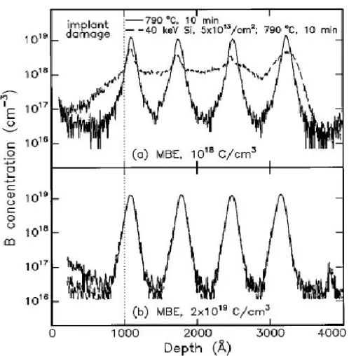
diffusion (TED) of boron incorporation of carbon above certain concentrations. Figure
1.11 shows boron concentration profiles before (solid line) and after the Si ion implant
anneal (dotted line) for two background carbon concentrations ((a): 1 10 /x 18 cm3 and (b):
19 3
2 10 /x cm ). In the sample with low carbon concentration (1 10 /x 18 cm3), boron profile are
observed to spread out post implant annealing (see dotted line in Figure 1.11(a)) due to
enhanced diffusion of boron, whereas in the sample with higher carbon concentration
(2 10 /x 19 cm3), (see Figure 1.11(b)), boron profiles stay pinned to their as implanted state –
Figure 1.11: Impact of carbon on boron diffusion: (a) Boron concentration profile spreads out post Si implantation anneal for a background carbon concentration of 10 /18 cm3, (b) No spreading in boron concentration profile is observed when the carbon concentration is increased to2 10 /x 19 cm3. [141]
In an alternate experiment, Simpson et al [131], have studied the effect of carbon
directly on dislocation formation during high temperature anneal following silicon ion
implantation onto silicon. They observed that carbon when incorporated onto the
substitutional sites leads to complete suppression of dislocation formation in silicon
during the anneal stage but has no effect when it occupies non-substitutional sites. In an
another study Cacciato et al[21], have observed both the suppression of TED of boron
and suppression of dislocation formation during post implant annealing by co-implanting
carbon with silicon at 900 oC. This could be due to the carbon atoms occupying the
Although it’s been postulated that inhibition of TED of boron is due to the
interaction of carbon with self-interstitial clusters in silicon, a complete mechanistic
picture is missing. Understanding the physics of how carbon interacts with self-interstitial
point defects and aggregates in silicon would result in better control over the boron
dopant profiles. This is particularly useful as the device dimensions continue to shrink.
1.4
Overall Computational Framework
Our aim is to understand the evolution of defects and defect clusters in silicon and
estimate the thermophysical properties for defect clusters under external conditions of
stress and temperature. Since the defects are very small in size (less than nm), a direct
measurement of the thermophysical properties of defect clusters is not possible using the
current experimental techniques. Fortunately a few simulation and modeling
methodologies have been developed over the last two decades that have captured the
physics under a physical phenomenon reasonably well. These techniques in turn have
been used extensively to model the material behavior under a given set of external
conditions and have resulted in significant gains in terms of product quality and safety of
processes. Depending upon the level of detail and accuracy one wants to achieve with
these simulations, the techniques can be broadly divided into four types.
At the most fundamental level is the ab initio approach that takes into consideration
both the atomic and electronic degrees of freedom. Electronic structure calculations have
been used extensively for estimating the defect structures, thermodynamic and transport
data.[7, 18, 47, 104] However the current computing power limit the ability of ab initio
simulations to O(100) atoms over timescale of O(10-12) sec.[55, 73, 156] and as a result,
it is almost difficult to study the dynamic aggregation of defects using this approach.
At the next level are the molecular dynamics and Monte Carlo techniques, which
use the empirical potentials to describe the interactions between the atoms. Within this
approach, the electronic degrees of freedom are averaged out and the behavior of atoms is
described using classical mechanics. This results in extending the computing limits to
O(106) atoms over time scales of O(10-9) sec. Various studies have been carried out using
the classical empirical atomic potentials to estimate various thermo physical properties of
defect and defect clusters, including formation energies and diffusivity , crystal structure,
and other transport properties.[8] This approach, based on classical empirical potential
offers the most versatile option; and has recently been extended by Manish and Sinno
[120-123] to develop a mechanistically consistent picture for aggregation physics of
vacancy clusters in Silicon wafer manufacturing.
Instead of simulating the interaction among all the atoms, coarse grained Kinetic
Monte Carlo (KMC), offers an alternate technique, where in only the interaction amongst
the defects (vacancies and interstitials) is simulated in the form of random sequence of
discrete diffusive and reactive events. This offers significant timescale advantage over
molecular dynamic and Monte Carlo techniques as the details of atomic vibrations are
coarse-grained while retaining the microscopic morphological information. The principal
drawback for KMC is that mechanistic information regarding rates for various events has
to supplied externally (using either of the approaches mentioned above). The KMC
evolution in crystalline materials such as metals and semiconductors. [13, 41, 75, 84,
103] Length scales of the order of 10-9 to 10-6 m and time scales of the order of 10-10 to
100 sec can be achieved using this technique.
If electronic calculations offer the most accurate description of the interaction
between atoms, then at the other end of spectrum is the continuum modeling approach,
which offers the most practical method in terms of computing time and length scale.
Continuum approach is based on conservation of mass, energy and momentum and is
numerically modeled using a series of finite difference and finite elements techniques.
Although the most practical from computing time perspective, but it suffers from the
same deficiency as KMC, in that the atomistic level of detail is lost and is only indirectly
captured in terms of parameters estimation.
Depending upon the objective, each of the approach offers an insight at different
level of detail. Past two decades of research, have in fact combined used two or more
methodologies to arrive at consistent picture of the physical phenomenon. For most of the
work done in this thesis we have used the molecular dynamics approach with empirical
interatomic potential, as it offers the best option for developing mechanistically
consistent picture for estimating the properties of small defect clusters and at the same
time helps us understand the evolution of aggregation process of defect clusters using the
same empirical interatomic potential and large scale parallel molecular dynamic
1.5
Thesis Objective and Outline
The objective of this work is two fold; the first is to develop computational tools to
extract the detailed atomistic information that can used to parameterize the continuum
models, and at the same time be able to directly simulate the physical phenomenon at the
atomistic level using large scale molecular dynamic simulations.
The second objective is to apply the computational tools we develop, to study the
physical phenomenon of aggregation of vacancy and interstitial aggregates in silicon, and
make a direct connection between the experiments and simulations.
The remainder of the thesis is organized as follows. In chapter 2 we introduce a
novel computational approach for probing the thermodynamics of defects in solids. We
use it to estimate the properties of vacancy clusters. The thermo-physical and
morphological properties of vacancy clusters evaluated from detailed atomistic
simulations are fed into the continuum model and a direct comparison is made to
experimentally observed properties like void nucleation temperature, void density, void
size distribution etc. Thus detailed atomistic parameters not just specify the parameters
for the continuum level simulations but also provide atomistic level details (mechanistic
information) about the physics of void aggregation. In chapter 3 we introduce the large
scale parallel molecular dynamics simulations approach to study the atomistic evolution
of interstitial clusters from small magic clusters to rod like defects to planar {113}, {111}
to large dislocation loops (FDL and PDL). A detailed aggregation landscape is proposed
as a function of external hydrostatic pressure and temperature. In chapter 4, we use the
developed in chapter 2 for vacancy clusters for studying individual interstitial clusters.
Using this method, a comprehensive picture for interstitial aggregation is proposed to
explain the evolution of dislocation loops, planar clusters and rod like large interstitial
clusters from small magic clusters, under given conditions of external pressure and
temperature. In chapter 5, we present a detailed quantitative model to describe the effect
of carbon on interstitial aggregation, by using large-scale atomistic simulations. Finally in
chapter 6, we summarize the conclusions of this work and suggest directions for future
2
Thermodynamic and Structural
Properties of Vacancy Clusters
Equation Section (Next)
Clustering of point defects and impurity atoms in crystalline materials is a ubiquitous
phenomenon that affects a host of material properties. The growth and processing of
crystalline semiconductor materials such as silicon, silicon alloys, and gallium arsenide,
for example, is almost completely dominated by rules aimed at minimizing the number of
defects such as point defect clusters [53, 132, 133], dislocations [36] and stacking
faults[126]. Similarly, in metal alloy systems, the microscopic distribution of the
component species can often critically affect the mechanical and chemical properties of
the alloy [151]. Given the importance of nucleation and growth of clusters in materials
processing, there has been much effort aimed at the development of simulation tools for
predicting the relationship between processing conditions and the resultant properties (i.e.
cluster size distribution) of a material [134]. Most such tools require as input the
thermodynamic properties of the various species in a system as a function of temperature
and cluster size and composition.
The properties of small atomic clusters, however, are extremely difficult to measure
experimentally. As a result, there has been substantial effort aimed at the structural and
thermodynamic characterization of clusters using atomistic simulations; for example
potentials [39, 120], tight-binding potentials [18, 19] and density functional theory [46,
96]. Much of the atomistic simulation work on cluster characterization has focused
exclusively on minimum energy configurations in order to make a thermodynamic and
structural description tractable. On the other hand, processing in both metallic and
semiconductor systems is often accomplished at elevated temperature where entropy can
be important, particularly vibrational and configurational entropy. In this work we
describe a novel framework (that inherently includes the vibrational and configurational
entropy) for estimating the free energy of point defect clusters in crystalline silicon, at
finite temperature based on an analysis of potential energy landscapes[68, 140] created
by clusters. We focus primarily on vacancy clusters in silicon using the
Environment-Dependent Interatomic Potential (EDIP)[14, 90] but show that our results and
conclusions are applicable to other types of clusters and (classical) potential systems and
therefore could have broad implications for the thermodynamic analysis of defects in
solids.
2.1
Thermodynamics of Cluster Aggregation Process
Single species aggregation is generally described by a series of coupled, reversible
interactions between clusters of different sizes.
( , )
( , )
K i j
i j i j
F i j
where, Xi is the concentration of clusters of size i, andK(i,j) and F(i,j) are the
coalescence and fragmentation kernels, respectively. Coalescence and fragmentation rates
depend on both kinetic and thermodynamic factors and the coalescence rate of clusters of
size i, and j. The coalescence kernel is given by
( ) ( , ) ( ) exp i j i j
ij i j
B G K i j A D D
k T
+ → +
⎛ ⎞
= + ⎜⎜− ⎟⎟
⎝ ⎠ (2.2)
where Aij is a size and morphology dependent geometric factor, Di is the mobility of
cluster i, and Gi j+ → +(i j) is the free energy barrier associated with the coalescence of
clusters i and j. The latter is usually expressed as [121]
2 ( )
1 ln( )
i j i j i j i j
G+ → + = ΔG+ − ΔG − ΔG −kT⋅ Ω
Ω (2.3)
where ΔGi is the formation free energy of a cluster of size i, relative to the perfect
crystal state. The last term in eq. (2.3) represents the change in the translational entropy
of the system associated with the coalescence event, where Ω1 and Ω2 are the initial and
final numbers of distinguishable ways of distributing clusters in a lattice containing N
sites for a given cluster size distribution [122]. As defined here, the translational entropy
only includes configuration space associated with the cluster centers-of-mass. Note that
for most systems of interest, the cluster size distribution is very dilute and spatial overlap
The free energy of formation of an atomic cluster of size iin a crystal can contain
several thermodynamic contributions,
i i i i
vib conf
G E T S TS
Δ = Δ − Δ − (2.4)
where i E
Δ is the formation enthalpy, i vib S
Δ the vibrational entropy of formation, and i conf S
the cluster configurational entropy. The indicate averaging over all the individual
configurations that the cluster can possess. The vibrational entropy of formation arises
because of the extra vibrational modes that are introduced as a result of the cluster. This
quantity can be computed directly with normal mode (quasi-harmonic) analysis [76]
and/or thermodynamic integration [57, 58].
The cluster configurational entropy is the number of distinguishable configurations
that a particular cluster can possess per lattice site. Note that the cluster configurational
entropy is fully excluded from the translational entropy as defined above and therefore
the total number of ways of distributing clusters in a lattice is given by
∏
Ω Ω = Ω i conf i transtot , where the product index is over all clusters in the system. While
the (ground state) vibrational entropy contribution in eq. (2.4) is usually accounted for in
calculations of the formation free energy of a solid cluster, the configurational entropy is
often neglected because it is difficult to estimate analytically except for very simple
structures. The concept of configurational entropy is described in more detail in the next
2.2
Vacancy Cluster in Silicon
Most continuum models for aggregation that require cluster thermodynamics as input
assume that the ground state morphology is a good approximation for describing the
properties of clusters as a function of size. For vacancies in silicon the ground state
morphology is the so-called Hexagonal Ring Cluster (HRC) configuration, which is
formed by maximizing the number of complete hexagonal vacancy rings [56]. Examples
of HRC structures are shown in Figure 2.1 for several cluster sizes. The HRC
morphology naturally evolves into regular octahedral structures with (111)-oriented
surfaces at larger sizes, and in this case the cluster configurational entropy can be
assumed to be negligible. These octahedral structures are frequently observed
experimentally with TEM in commercial crystalline silicon [82].
Figure 2.1: Hexagonal ring clusters (HRC) containing (a) 6, (b) 10, and (c) 14 vacancies.
While the HRC morphology is a reasonable representation of large clusters at low
temperatures, much of semiconductor processing (and obviously crystal growth) takes
place at high temperatures. Previous atomistic simulations by Prasad and Sinno, [121,
122] employing the classical EDIP potential [14] demonstrate clearly that vacancy
clusters at elevated temperature spend a majority of the time in spatially extended
configurations that are much higher in energy than the ground state. The fact that vacancy
clusters can assume these extended configurations arises from the large vacancy-vacancy
interaction distance, which has been shown to extend up to about 7.8 Ǻ, which
corresponds to the 4th neighbor shell along the (110) direction (4NN-110) or the 8th
-nearest neighbor shell overall [122]. The driving force for this behavior is now known to
be a combination of vibrational and configurational entropy. Only the former has been
considered in previous thermodynamic models and it is shown in the following sections
that the configurational entropy at high temperature not only dramatically influences the
thermodynamics of clusters, but also the aggregation kinetics through a modification of
the effective capture radius.
2.2.1 Configurational Entropy
As pointed out in section 2.1, the configurational entropy of a system consists of two
terms, the translational and (internal) configurational part, with total number of
configurational states given by i tot trans conf
i
Ω = Ω
∏
Ω . The nature of these terms isdemonstrated in Figure 2.2 for the case of a dimer (two vacancies located next to each
other) on a two-dimensional (9x9) cubic lattice. For such a system consisting of only the
dimer, the total number of states reduces toΩ = Ωtot transΩconf , with Ω =tot 81 2x being the
therefore has 2 distinct (energetically degenerate) configurations per lattice site; i.e.
2
=
Ωconf .
Figure 2.2: (a) Centres of mass of several dimmers on a two dimensional lattice (left). (b) Full center-of-mass lattice for dimmers is twice as dense as that of actual lattice (right).
The situation is far more complex for “real” vacancy clusters in the tetrahedral
silicon lattice for several reasons. The first is that long-ranged vacancy-vacancy
interactions (up to the 4th nearest neighbor along the (110) directions, or about 7.8 Å) The
effect of long-ranged interactions on the cluster configurational entropy is shown in
Figure 2.3 in which the schematic dimer shown in Figure 2.2 can now exist in 2nd-nearest
neighbor (2NN) configurations as well as the 1NN configuration. The center-of-mass
lattice now contains three sites for each of the actual lattice sites and Ωconf =3 for this
that of the 1NN configuration and the microcanonical expression for the entropy is no
longer valid because the system has different energy states.
Figure 2.3: (a) Centers of mass of 1NN and 2NN dimers on a two-dimensional lattice (left). (b) Full center-of-mass lattice for 1NN and 2NN dimmers (right).
A second source of large configurational entropy is that cluster configurations in
the silicon lattice are not limited to on-lattice structures because lattice atoms can relax
around the cluster in a variety of configurations. Both these issues will be discussed
2.3
Cluster Formation Thermodynamics from Potential Energy
Landscape
In the following discussion we employ the concept of inherent structures (IS) in a
potential energy landscape (PEL) in order to describe the thermodynamics of defect
clusters in a crystal. Inherent structures, as introduced by Stillinger and Weber [138], are
local minimum configurations in the 3N-dimensional potential energy surface [68]
defined by the coordinates of an N-atom system. A basin is defined as the set of points in
phase space that map to the same IS when the system is quenched using local energy
minimization. The basin construct is useful because it partitions the total phase space of
the system into a set of non-overlapping local minima connected by saddle points which
permit basin-to-basin hopping. At sufficiently low temperature, the system will spend the
majority of time in any given basin and only occasionally be able to pass through to
another basin (i.e. the basin-to-basin motion is a rare event).
The concepts of inherent structures and potential energy landscapes have existed for a
long time [68] and have recently been successfully applied to the study of configurational
entropy in supercooled liquids and glasses [128, 129]. In these studies, long equilibrium
MD trajectories were periodically quenched to locate the potential energy basins, which
were then used to compute thermodynamic properties as shown below. Because of their
disordered nature, supercooled liquids and glasses possess a large number of inherent
structures, and at sufficiently low temperatures, the basin-hopping picture has been shown

![Figure 1.3: Feature length Time Line from Intel [5]. Numbers on curve indicate the transistor gate oxide thickness in nm](https://thumb-us.123doks.com/thumbv2/123dok_us/9258465.1463825/27.612.132.518.70.288/figure-feature-length-intel-numbers-indicate-transistor-thickness.webp)
![Figure 1.6: TEM Images of an octahedral void. [154]](https://thumb-us.123doks.com/thumbv2/123dok_us/9258465.1463825/33.612.231.418.71.281/figure-tem-images-an-octahedral-void.webp)