•••• • •••
fr-• • • •
...
• • • •
&A7
. . .
A&
~
[I
Systematics General l:orporation
TABLE OF CONTENTS
Paragraph
Section I - Specification
Introduction --- 1-1
T-5l0l Specification --- 1-3
Section II - Programming
Microcontroller Programming -Instruction Set for T-5l0l Microcontroller ---Flag Control ---Literal Control --Asynchronous Receiver/Transmitter Control ---Transmission Longitudinal Checking ---Tri-State Bus Control ---Display Control ---Utility Register Control
---Section III - Theory of Operation
Introduction ---Cathode Ray Tube Display ---Quick Reference Guide ---Main Circuit Board ---Power Supply ---Keyboard ---.---Normal Keyboard Operation ---Escape Sequences ---Formatting Aids ---Data Editing Operation ---Data Interface ---Data Transmission ----Special Function Keys ---Status Displays
---Section IV - Monitor Description
2-1 2-12 2-23 2-24 2-25 2-25 2-25 2-26 2-27 3-1 3-1 3-3 3-5 3-5 3-6 3-6 3-12 3-12 3-14 3-18 3-18 3-21 3-21
Monitor Electrical Specifications --- 4-1
Data Display Specifications --- 4-2
Environmental Specifications --- 4-3
Human Factors Specifications --- 4-3
Controls --- 4-3
Theory of Operation --- 4-6
Section V - Maintenance and Failure Analysis
Care of the T-5l0l
---External Adjustments
--~---Disassembly ---Internal Adjustments ---Philosophy of Failure Analysis ---Troubleshooting the Display Maintenance of Main Logic Board and Power Supply
TABLE OF CONTENTS (cont)
Paragraph
Section VI - Scheduled Maintenance
Scheduled Maintenance --- 6-1
Safety Precautions --- 6-7
Section VII - Schematic Drawings and Diagrams --- 7-1
Table 2-1 2-2 2-3 2-4 2-5 2-6 2-7 2-8 2-9 2-10 2-11 3-1 3-2 3-4 3-5 3-6 3-7 3-8 4-1 4-2 5-1 5-2 5-3 5-4
LIST OF TABLES
T-5l0l Functional Units Table of Register Usage ---T-5l0l Instruction Set ---Random Access Memory Control ---RAM Address Control ---ROM Instruction Execution Sequence Control ---Table of Conditions ---Table of Condition Significance ---Table of Flags ---Asynchronous Transmitter/Receiver Control ---Tri-State Bus Control
---Keyboard Operation ---Binary Codes ---Formatting Aids ---Absolute Cursor Positioning ---Block Transmission Control ---Special Functions ---Status Displays
---Input Data Specifications -CRT Display Specifications
---Baud Rate Selections --- ---T-5l01 Failure Analysis Guide Logic Board Terminal Identification Chart ---Tri-State Bus Location
Figure 1-1 2-1 2-2 3-1 3-2 3-3 4-1 5-1 5-2 5-3 5-4 5-5 5-6 5-7 5-8 5-9 5-10 5-11 5-12 5-13 5-14 6-1
LIST OF FIGURES
T-5l0l Interactive Display Terminal
---T-5l0l Data Flow Block Diagram ---T-5l0l Asynchronous Receiver/Transmitter
---T-5l0l Functional Block Diagram ---Character Format ---Keyboard
---Synchronization and Blanking Generator Waveforms
External Controls ---Video Shield Retaining Screws ---Rear Cover Retraining Screws ---Logic Assembly Interconnections ---Logic Power Supply Shields ---Logic Power Supply ---Video Enclosure Chassis Cabling --Internal Controls ---CRT Mounting (Right Side) ---CRT Mounting (Left Side) ---Voltage Waveforms for Display Video Circuit Board Component Location ---Main Logic Board Layout
---Program Display
---7-1 thru
Page 1-2 2-1 2-3 3-2 3-4 3-7 4-5 5-2 5-4 5-5 5-6 5-8 5-9 5-10 5-11 5-14 5-15 5-16 5-12 5-24 5-30 6-6
7-21 Schematics -7 Configuration --- 7-3
7-22 thru
7-44 Schematics -13 Configuration
---7-45 thru
7-46 Keyboard Schematic
---7-47 7-48 7-49 7-50 7-51 7-52 7-53
Keyboard Interface Assembly
---Wiring Diagram ----Logic Power Supply ---Wiring Pk1ll2 --Video Schematic ---Video Wiring ---Power Supply Layout
SECTION I
T-SIOI Specification
INTRODUCTION
The purpose of this manual is to provide operation and maintenance information for the T-SIOI Interactive Display Terminal.
The scope of the material provided is sufficient in all aspects of operation and maintenance of the equipment.
The T-SIOI consists of cable-interconnected assemblies. This unit is in turn connected to a computer by an additional interface cable.
The T-5101 Interface Display Terminal is shown in Figure 1-1.
(
(
I
T-5l0l SPECIFICATIONS
Display
80 Character Lines 24
Character positions 1920
Character Set 96 ASCII {Upper Case}
Screen Phosphor White (P4)
Face Plate Etched
Refresh Rate 60 pages/Second
Protected Fields Reduced Intensity
Status Displays 8
Control Characters Display 31
Blinking Field Rate 4 per second
Security Fields Display Suppressed
Page Roll Up
Cursor
Format
Controls
Data Transmission
Code
Parity
Reverse Video Block
Forespace, Backspace Upline, Downline, New Line, Return, Home, Tab
Backtab, position
Addressing, Position Reading
Asynchronous ASCII 10 unit code
Even
Data Transmission
Interface
Rates
Duplex
Modes
Keyboard
RS-232-C
110, 150, 300, 600, 1200, 2400, 4800, 9600 Baud
Full and Half
Conversational Block
Line, Page or Message (all or foreground)
construction Separate
Character and Control Keys 68
Cursor and. Format Keys 14
Numeric Keys Pad 14
Function Keys 16
Transmission Send Control
Keys Page, Line, Message
Interlocking Two Key rollover
Key Operation 2 ounce
Lighted Mode Keys Shift Lock, Write Protect
Program, Conversation, Page Edit
Memory
Storage Capacity
Security Locations
Control Character Storage
1920 Characters
Display Suppressed
Memory
Protected Fields Character Protect Bit
Data Editing
Keyboard Editing
Character Type over, Insert, Delete
Line Insert, Delete, Erase to
End of line
Page Clear all or foreground
to NUlls or Spaces, Erase to End of Page (Replace Allor Foreground with NUlls or Spaces)
Protected Fields Reduced Intensity
Computer Controlled Editing All of Above with Receipt of ESC Sequences
Tempest
Complies with NACSEM 5100, As Modified By AFNAG-9A
Physical Characteristics
Dimensions
Display
Keyboard
Weight
A-C Power Requirement
Environment
l4.12"H X 20.S"W x l8"L
4"H X 20.S"W x 9"L
55 Ibs.
115 Volt, 60 Hz
c 0
5-50 C; 41-122 F
5-95% Relative Humidity without Condensation
SECTION II
MICROCONTROLLER PROGRAMMING
The organization of data transmission and control for the T-5101 interactive data display terminal is given in the data flow block
diagram, Figure 2-1 below. A detailed description of control
and programming for the microcontro11er follows. Specific details
of the terminal logic and control devices are contained in schematic drawing 129361, sheets 7-1 through 7-22, contained in Section 7.
FROM:
1
KEYBOARDJ
MEMORY
i
DISPLAYSECTION 1 - - - , -.. SECTION
(RAM)
CONTROL SECTION
ROM
~---ASYNCHRONOUS RECEIVER TRANSMITTER
t
o:
1 -... IDEO
ONITOR
INTERFACE TO/FROM:
--t'COMPUTER and/or li,RINTER
Figure 2-1. T-5101 Main Circuit Board
Data Flow Block Diagram
T-5101 Data oraanization is based on random access memorv time sharina
between control section and display section, with the di~p1a·y
section given highest priority for the refresh function and the
control section given secondary priority. The display function
utilize random access memory 27% of the time leaving 73% for the
control functions. This sharing organization provid~s the T-5101
Data information and control commands between the various logic sections and
(memory, control, timing) bus.
are transferred internally components over a tri-state
Keystroke signals enter the main logic board as 8 bit parallel data
codes, along with strobe signals. However, data received from an
interfacing computer is received as ASCII seven bit serial data. The logic board has a serial-parallel converter to translate serial ASCII codes to parallel codes as well as a FIFO buffer to allow time for operations which are longer than inter character intervals in fast transmission rate environments.
The transmitter/receiver is an LSI/UART chip which (I) accepts
serial ASCII 10 or 11 unit codes (word structure option is strappable)
from an RS-232-C standard interface or 20 rna current loop optional interface and (2) transmits an equivalent 8 bit parallel code as
a data word to the control section. Furthermore, the universal
asynchronous transmitter/receiver (UART) also decodes 8 bit words received from the T-SlOl control section and transmits serial ASC II
over the data signal interface. See Figure 2-2 for additional
details of the UART.
Information transfer is controlled in the T-SlOl by the microcontrol
logic commanded by codes stored in a preprogrammed ROM. The standard
T-5l0l terminal functions are contained in four pages (256-8 bit words/pages) of microcode, with printer extension option requiring an additional page, and terminal polling option needing two pages.
The display memory section consists of 16 random access memory (RAM)
chips, providing storage capacity of 2048 8-bit words. This memory
provides useful character storage of 1920 characters, 24 lines of
80 characters each. The memory section also contains conversion
logic necessary to monitor display cursor position.
The display section consists of four main subsections, i.e.,
(1) Character Generator, (2) RoW Refresh Logic, (3) Cursor Display
Logic, and (4) Timing Control. In addition to the above functions,
display section also provides control for reduced luminance (protected fields) and 8-status indicator displays.
Actual registers used in the T-5l01 micro controller code are s~
marized and listed in Table 2-2.
VSS l1i _ ~
VOD 131
~
...
VGG 121
.
~ T"""'SAlIJl E" HOLDINGP,[GI:'if[R
'RC
1001
LOAD 1211 THAl
TIMtNG THRI
l.O 1211 tOlHROl
SID
SHIFT 1141 TR!
~-+---. ~?
PI
EPE
WORO LENGTH SElECT
~s~ < > M r
-I~JP!JT STRUCTURE
MOS DEVICE "Au ACTS AS AN INTERW>.L PUU.·Up RESISTOR TO V~;S ~ Vce WHICH SIASES OFf THE CASCODE DEVICE OF THE TTL OUTPUT IN THE HIGH·l::VEL OUTPUT STATE. IN TilE LO'N·LEVEL OUTPUT ST t.TE THE TTL OUTPUT DE· VICE SIN:<S THE CURHENT SUF'?UED BY DEVICE "Au.
P!
lUI FE lUI
NOTE: ~ TRI·STAT-E OUTPUT
Vee
' - - - v - - - - '
lnlCAl nL OllT'eT
I
Vss (lVISTRATEl· vee
---1---' _ - y - - J
T~t4~lA INPUT
I
~--..,_--J ' - - - y - - '
TR1telA OVT1UT TYriCAl n l
IN?UT
DATA RECEIVED
DEUCl
DR 1191
Sf 0
ORR
1111
OUTPUT STR!JCTURE
[image:13.624.116.525.5.736.2]PIN NUMBER 1 2 3 4 5-12 13 NAME
VSS POWER
VGG POWER
VDD POWER
RECEIVER REGISTER DISCONNECT RECEIVER HOLDING REGISTER DATA SUPPLY SUPPLY SUPPLY
PARITY ERROR
SYMBOL VSS VGG VDD RRD RRS RRl PE FUNCTION
+5 volts Supply
-12 volts Supply
Ground
A high-level input voltage. VIH applied to this line
disconnects the RECEIVER
HOLDING REGISTER outputs from
the RRS-RR
t
data outputs(pins 5-12 •
The contents of the RECEIVER HOLDING REGISTER appear on these lines in parallel if a low-level input voltage, VIL , is applied to RRD.
Program control selection of a word length less than eight
(S) bits will cause the most significant bits of the
character to be forced to a 1ow-level output voltage, VOL.
The character will be right
justified. RRl (pin 12) is
the least significant bit of the character.
The status of the parity verification circuit appears on this line, i f a low-level input voltage, VIL , is applied to the STATUS FLAGS DISCONNECT
(pin 16) control line. Wired
OR capability is provided on this line allowing PE lines
from other arrays to be OR
tied. A high level ou~put
voltage,VOHI on this line (under the conditions above)
Figure 2-2. T-5l0l Asynchronous Receiver/Transmitter (UART) (Continued)
PIN NUMBER
14
15
FRAMING ERROR
OVERRUN ERROR
SYMBOL
FE
OE
FUNCTION
indicates a PARITY ERROR in the received parity bit as programmed by the EVEN PARITY ENABLE control line
(pin 39). The status is
updated each time a charac-ter is transferred from the RECEIVER REGISTER to the RECEIVER HOLDING REGISTER.
The status of the STOP bit detection circuit appears on this line if a low-level input voltage, VIL' is
applied to the STATUS FLAG DISCONNECT (pin 16) control
line. Wired OR capability
is provided on this line allowing FE lines from other
arrays to be OR tied. A
high-level output voltage, VOH' indicates that the received character has no valid STOP bit, i.e., the bit following
the parity bit is not a high-level input voltage, VIH •
The status of the DATA RECEIVED circuit appears on this line of a low-level input voltage, VIL' is applied to the STATUS FLAG DISCONNECT (pin 16) control
line. Wired OR capability is
provided on this line allowing OE lines from other arrays to
be OR-tied. A high level
out-put voltage, VOH, indicates that the previously received charac-ter was not read (DR line not reset) before the present character was transferred to the RECEIVER HOLDING REGISTER.
PIN NUMBER 16 17 18 19 20 21 22
STATUS FLAGS DISCONNECT
RECEIVER REGIS-TER CLOCK
DATA RECEIVED RESET
DATA RECEIVED
RECE IVER INPUT
~STER RESET
TRANSMITTER HOLDING REGISTER EMPTY SYMBOL SFD RRC ORR DR RI MR THRE FUNCTION
A high-level input voltage, VIH , applied to this pin disconnects the PE, FE, OE, DR and THRE circuit outputs.
This clock is sixteen (16) times faster than the desired receiver shift rate.
A low-level input voltage, VIL , applied to this line resets the DR line.
A high level output voltage, VOH' indicates that an entire character has been received and transferred to the
RECEIVER HOLDING REGISTER.
Serial input data received on this line enters the RECEIVER REGISTER at a point determined by the character length, parity, and the number of stop bits. A high-level input voltage, VIH , must be present when data is not being received.
This line is strobed to a high-level input voltage, VIH , to clear the logic after power
turn-on. It resets all registers
and sets the serial output line to a high-level output voltage. VOH·
A high-level output Voltage, VOH ' on this line indicates the
TRANSMITTER HOLDING REGISTER has transferred its contents to the TRANSMITTER REGISTER and may be loaded with a new character.
Figure 2-2. T-5l0l Asynchronous Receiver/Transmitter (UART) (Continued)
PIN NUMBER
23
24
25
NAME
TRANSMITTER HOLDING REGISTER LOAD
TRANSMITTER REGISTER EMPTY
TRANSMITTER REGISTER OUTPUT
SYMBOL
THRL
TRE
TRO
FUNCTION
A low-level input voltage, VIL , applied to this line enters a character into the TRANSMITTER HOLDING REGISTER. A transition from a low-level
input voltage. VIL , to a high
level input voltage. VIH,
transfers the character into the TRANSMITTER REGISTER if i t is not in the process of
trans-mitting a character. If a
character is being transmitted, the transfer is delayed until its transmission is completed. Upon completion, the new charac-ter is transferred simultaneously with the initiation of the
serial transmission of the new
character.
A high-level output voltage. VOH • on this line indicates that the TRANSMITTER R::;GISTER has completed serial transmission of a full character including
STOP bit(s). It remains at this
level until the start of trans-mission of the next character.
The contents of the TRANSMITTER REGISTER (START bit DATA bits, PARITY bit, and STOP bit), are serially shifted out on this
line. This line will remain
at a high level output voltage, VOHQ when no data is being
transmitted. A start of
mission is defined as the trans-ition from a high-level output voltage, VOL' of the start bit.
PIN NUMBER
26-33
34
35
NAME
TRANSMITTER REGISTER DATA INPurS
CONTROL REGISTER LOAD
PARITY INHIBIT
SYMBOL
CRL
PI
FUNCTION
Parallel 8-bit characters are input on these lines into the TRANSMITTER HOLDING REGISTRR
with THRL Strobe. If a
charac-ter of less than 8 bits has
been selected (by WLSl and WLS2), the least significant bits only
are accepted. The character is
right justified into the least
significant bit. A high-level
input voltage, VIH , will cause a high-level output voltage, VOH ' to be transmitted.
A high-level input voltage,
V , on the line loads the
C6~TROL
REGISTER with thecontrol bits (WLSl' WLS 2 , EPE,
PI, SBS). This line may be
strobed or hard wired to a high-level input voltage,
VIH-A high-level input voltage, VIH , on this line inhibits the parity generation and verification
circuits. The STOP bites) will
immediately follow the last data bit on transmission if parity is
uninhibited. A low-level input
voltage, VIL , enables the
parity generation and
verifica-tion circuits_ PI will, when a
high-level input voltage, VIH , is applied, also clamp the PE line
(pin 13) to a low-level output voltage,
VOL-36 STOP BIT(S) SBS This line selects the number of
SELECT STOP bits generated after the
PARITY bit durinJ transmission. A
high-level input voltage, VIH , on this line selects two STOP bits, and a low-level input voltage, VIL , selects a single STOP bit.
Figure 2-2. T-5l0l Asynchronous Receiver/Transmitter (UART) (Continu~d)
PIN NUMBER
37-38
39
40
WORD LENGTH SELECT
EVEN PARITY ENABLE
TRANSMITTER REGISTER CLOCK
SYMBOL
EPE
TRC
FUNCTION
These two lines select the
character length to be 5, 6,
7, or 8 bits.
WORD LENGTH
5 bits
6 bits
7 bits
8 bits
This line selects either even or odd PARITY to be generated by the transmitter and checked by
the receiver. A high-level input
voltage, VIH' selects even PARITY and a low-level input voltage, V1L , selects odd PARITY.
This CLOCK is sixteen (16) times faster than the desired trans-mitter shift rate.
Figure 2-2. T-5101 Asynchronous Receiver/Transmitter (UART) (Continued)
Information is transferred between functional units by way of the
tristate bus, TSB, under microprogram control. This information
[image:19.620.51.582.61.473.2]Unit Mnemonic
RCV
KEY
CPR
CPC
LIT
RDR
WDR
LRC
ADD
MACR
INPUT
OUTPUT
CMD
MAR
INn
CNTR
TABLE 2-1. T-S10l FUNCTIONAL UNITS
From
From
From
From
From/To
From
To
From/To
From
From/To
From/To
From/To
From/To
Unit
External Serial Source via UART Receiver
Keyboard
Cursor position row register
Cursor position character register
Eight bit literal register
Random access page buffer via the Read Data Register
Random access page buffer via the write Data Register
Modulo 2 adder and accumulator (7 bits)
Switch (8 bits) internal, manually set
Random access page buffer row counter (address register high order five bits)
Utility Register*
Utility Register*
Utility Register*
Margin Register
Indicator Register
Counter Register
* Unused in Standard T-S101
•
Register Symbol
WDR
RDR
MACC
MACR
ARTO
ARTl
LIT
CPR
CPC
KEY
LRC
RCV
TABLE 2-2. TABLE OF REGISTER USAGE
Register Name
Write Data Register
Read Data Register
Memory Address Counter Character
Memory Address Counter Row
Communications Interface UART
Auxiliary Interface UART (printer, etc.)
Literal (8 bit) Register
Cursor Row Position Register
Cursor Character Position Register
Keyboard Register
Longitudinal Transmissions Check Register
Receiver
Description
Eight bit character register contains characters to be written into the R.A.M. from
tri state bus.
Eight Bit register to con-tain characters read from the R.A.M. for transfer to tri state bus.
Contains low order 7 bits of
the R.A.M. address accessible to the tri state bus (column).
contains high order 5 bits of
the R.A.M. address accessible to the tri state bus (row).
Used to transfer constants from ROM to tri state bus.
For modulo 2 sum check of transmission characters.
Register Symbol
ADD
MAR
CNTR
IND
CMD
OUTPUT
INPUT
TABLE 2-2. TABLE OF REGISTER USAGE (Continued)
Register Name
Margin Register
Counter Register
Indicator Register
Conunand Register
Output Register
Input Register
Description
switches set manually inside cabinet
Eight bit utility register used for temporary holding of dynamic data.
Eight bit utility register used for holding program counter during subroutine calls, and for incremented or decremented comparisons.
Eight bit register controls lighted indicators at right hand side of screen.
1 = lighted ••
Not used in standard MMDC.
Not used in standard MMDC.
Not used in standard MMDC.
INSTRUCTION SET FOR T-5l0l MICRO CONTROLLER
Instructions may be partitioned into two classes, those which occupy
two eight bit bytes and those which occupy one eight bit byte. These
can be represented as six or three octal digits, respectively, where
the high order bit in each word is assumed to be zero. The implied
ninth bit is, of course, not actually present in the eight bit hardware.
high order word low order word (if required)
I
I
I
I
[image:22.618.44.574.72.471.2]Where Di . is the jth octal digit for the ith 8 bit word. , J
Subfields of instructions will be indicated by only the high order
and low order octal digits in parentheses, for example: Only
high order word:
or both high and low order words:
J
Examples of terminal control functions written in the T-S10l mnemonic instruction set are given at the conclusion of this section.
TABLE 2-3. T-5101 INSTRUCTION SET
001 READ 072 CLR STB6 220 JFC OFLO
003 WRITE 073 SET STB6 221 JFC MAC=CPR
004 CLR WDR 074 CLR STB7 222 JFC OPTI
005 LOA WDR 075 SET STB7
006 SET WPROT 076 CLR STB8 230 JFC RDR
007 CLR WPROT 077 SET STB8 23il. JFC RPE
016 SET PROTM 100 JMP 232 JFC RFE
017 CLR PROTM 120 SEL ARTO 234 JFC THRE
020 CLR MACC 121 SET RTSO 235 JFC CTS
021 LOA MACC 122 CLR RTSO 236 JFC TRE
022 SET MACC 123 LOA ARTO 237 JFC NORS/OPT2
023 INC MACC 124 CLR ARTO 240 JFC PROTM
024 DEC MACC 130 SEL ARTI 241 JFC PROT
027 LOA CPR 131 SET RTSI 242 JFC INTIN
030 CLR MACR 132 CLR RTSI 243 JFC FULL
031 LOA MACR 133 LOA ARTI 243 JFC KEYST2
032 SET MACR 134 CLR ARTI 244 JFC OPNC
033 INC MACR 150 LOA LIT 244 JFC RESET
034 DEC MACR 156 CLR LRC 245 JFC CONV
035 INH CUR 157 CLK LRC 246 JFC FDX
036 ENA CUR 160 TSB=RDR 247
037 SET BEEP 161 TSB=KEY
040 LOA OUTPUT 162 TSB=RCV 250 JFC MACC
042 LOA MAR 163 TSB=LIT 251 JFC NULL
044 LOA IND 164 TSB=CPC 252 JFC LIT7
045 CLR INn 165 TSB=CPR 253 JFC LIT8
046 LOA CMD 166 TSB=LRC 260 JFC STBI
051 LOA CNTR 261 JFC STB2
052 INC CNTR 170 TSB=ADD 262 JFC STB3
053 DEC CNTR 172 TSB=INPUT 263 JFC STB4
054 SET TIME 173 TSB=MAR 264 JFC STBS
055 SET BIN 174 TSB=INn 265 JFC STB6
056 CLR RTSEN 175 TSB=CNTR 266 JFC STB7
057 SET RTSEN 200 JFC TSBI 267 JFC STB8
060 CLR STBI 201 JFC TSB2 300 JTC TSBI
061 SET STBI 202 JFC TSB3 301 JTC TSB2
062 CLR STB2 203 JFC TSB4 302 JTC TSB3
063 SET STB2 204 JFC TSB5 303 JTC TSB4
064 CLR STB3 205 JFC TSB6 304 JTC TSB5
065 SET STB3 206 JFC TSB7 305 JTC TSB6
066 CLR STB4 207 JFC TSB8 306 JTC TSB7
067 SET STB4 210 JFC KEYSTR 307 JTC TSB8
070 CLR STB5 213 JFC CALL 310 JTC KEYSTR
071 SET STB5 214 JFC RTN 313 JTC CALL
)
[image:24.613.58.572.63.679.2]TABLE 2-3. T-5101 INSTRUCTION SET (Continued)
!
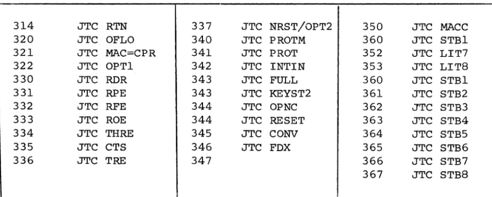
314 JTC RTN 337 JTC NRST/OPT2 350 JTC MACC
320 JTC OFLO 340 JTC PROTM 360 JTC STB1
321 JTC MAC=CPR 341 JTC PROT 352 JTC LIT7
322 JTC OPT1 342 JTC INTIN 353 JTC LIT8
330 JTC RDR 343 JTC FULL 360 JTC STB1
331 JTC RPE 343 JTC KEYST2 361 JTC STB2
332 JTC RFE 344 JTC OPNC 362 JTC STB3
333 JTC ROE 344 JTC RESET 363 JTC STB4
334 JTC THRE 345 JTC CONV 364 JTC STB5
335 JTC CTS 346 JTC FDX 365 JTC STB6
336 JTC TRE 347 366 JTC STB7
367 JTC STB8
[image:25.623.42.549.60.263.2].-TABLE 2-4.
Mnemonic
READ 001
WRITE 003
LOA WDR 005
CLR WDR 004
TSB=RDR 160
SET WPROT 006
CLR WPROT 007
SET PROTM 016
CLR PROTM 017
RANDOM ACCESS MEMORY CONTROL
Description
Transfers the contents of the RAM location indicated by the contents of MACR, MACC into the RDR
Transfers the contents of the WDR into the RAM location indicated by the contents of MACR, MACC
Replaces the contents of the WDR with the contents currently on
the TSB
Clears the WDR
Sets the contents on the TSB equal to the contents of the RDR
Sets the write protect bit on all words subsequently written into
the RAM
Clears the write protect bit on all words subsequently written into the RAM
Set the PROTM. This status bit
is used as a global condition by the program to disable the over-writing of any characters in the RAM for which the WPROT bit is set
Clear the PROTM. This global
condition enables the overwriting of write protected characters
TABLE 2-5.
Mnemonic
CLR MACC 020
CLR MACR 030
LOA MACC 021
LOA MACR 031
LOA CPR 027
SET MACC 022
SET MACR 032
INC MACC 023
INC MACR 033
DEC MACC 024
DEC MACR 034
SET BIN 055
RAM ADDRESS CONTROL
Description
Set character counter to left margin
Set row counter to top row
Set character counter to value on tri state bus
Set row counter to value on tri state bus
Sets contents of CPC and CPR equal to current contents of MACC and MACR, respectively
Set character counter to right margin
Set row counter to bottom row
* Move character counter right
one position
*
Move row counter down one line*
Move character counter leftone position
*
Move row counter up one lineThis instruction, if followed immediately by LOA MACC or LOA MACR, will load the binary value of the (TSB) rather than the interpreted character value normally loaded.
*
These operations will set OFLO if they cause character address toTABLE 2-6.
Mnemonic
JMP
JTC
JFC
ROM INSTRUCTION EXECUTION SEQUENCE CONTROL
lOP LLL
3CC LLL
2CC LLL
Description
Causes next instructions to be taken from the location indicated by LLL on page P
Causes next instructions to be taken from the location indicated by LLL on the local page if the condition indicated by CC is true. rnstructions are taken in normal
sequence otherwise. (See table
of conditions for values of CC.) (See note below for CALL and RTN.)
Causes next instriuctions to be
taken from the location indicated by LLL on the local page if the condition indicated by CC is false. Instructions are taken in normal
sequence otherwise. (See table
of conditions for values of
ce.)
(See Note below for CALL and RTN.)
(NOTE: Transfer of control to subroutines on the same page
are facilitated by the CALL and RTN conditions as follows: )
JFC CALL 213
JFC RTN 214
2-18
Causes contents of the program counter to be transferred to CNTR prior to transfer of control
Causes contents of CNTR to replace contents of program
counter. LLL is ignored. CNTR
TA3LE 2-7. TABLE OF CONDITIONS
Condition
Mnemonic Identifier Description
TSBl 00 Tri State Bus Bit 1
2 01 Tri State Bus Bit 2
3 02 Tri State Bus Bit 3
4 03 Tri State Bus Bit 4
5 04 Tri State Bus Bit 5
6 05 Tri State Bus Bit 6
7 06 Tri State Bus Bit 7
8 07 Tri State Bus Bit 8
KEYSTER 10 Keyboard strobe
OFLO 20 MACC/MACR overflow or underflow
MAC=CPR 21 Set if MACR equals CPR
OPTI 22 Wire straps on main logic board
PROTM 40 Set if in character protection
mode
PROT 41 Character protect bit in RAM and
protect mode
CONV 45 Conversation mode
CALL 13 Subprogram call
RTN 14 Subprogram return
RDR 30 RCV Data ready
RPE 31 RCVR parity error
TABLE 2-7. TABLE OF CONDITIONS (Continued)
- - - : - - - : - - - _
..Mnemonic
ROE
THRE
CTS
TRE
RESET/OPT2
INTIN
KEYST2
RESET
FDX
MACC
NULL
LIT7
LIT8
STBl
2
3
4
5
Condition Identifier
33
34
35
36
37
42
47
44
46
50
51
52
53
60
61
62
63
64
2-20
Description
RCVR overflow
Transmitter holding register ready
Clear to sent (asynchronous transmission)
Transmitter register empty
Reset by OPT 2 (Strap)
Extended memory option
Send Key Strobe Line (operation keys)
Reset key (also used with extended memory)
Full duplex
(TSB) equals (MACC)
(TSB) equals (NULL)
(TSB) equals (LIT) seven bits
only (1 through 7)
(TSB) equals (LIT) eight bits
Status BIT 1
Status BIT 2
Status BIT 3
Status BIT 4
TABLE 2-7. TABLE OF CONDITIONS (Continued)
i .
-Condition
Mnemonic Identifier Description
6 65 Status BIT 6
7 66 status BIT 7
8 67 status BIT 8
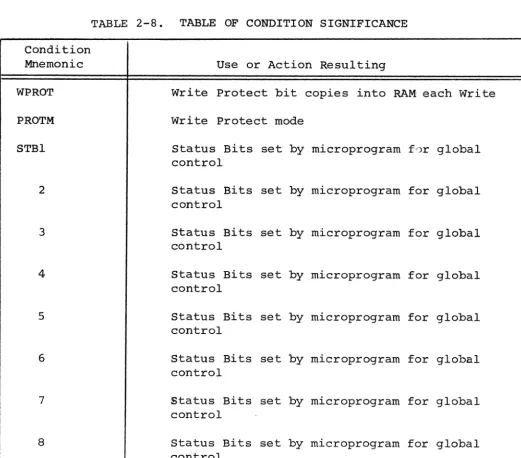
TABLE 2-8. TABLE OF CONDITION SIGNIFICANCE
Condition
Mnemonic Use or Action Resulting
WPROT write Protect bit copies into RAM each Write
PROTM Write Protect mode
I STBl Status Bits set by microprogram for global
" control
2 Status Bits set by microprogram for global
control
3 Status Bits set by microprogram for global
control
4 Status Bits set by microprogram for global
control
5 Status Bits set by microprogram for global
control
6 Status Bits set by microprogram for global
control
7 status Bits set by microprogram for global
control
8 Status Bits set by microprogram for global
[image:31.627.47.569.246.704.2]TABLE 2-8.
I Condition
Mnemonic
RTSO
RTSl
TSBl
2
3
4.
5
6
7
8
KEYSTR
CALL
RTN
RDR
RPE
THRE
CTS
TRE
TABLE OF CONDITION SIGNIFICANCE (Continued)
,
Use or Action Resulting
Request to sent (Main ART)
Request to send (Auxiliary ART)
Tri State Bus Bits
Tri State Bus Bits
Tri State Bus Bits
Tri State Bus Bits
Tri state Bus Bits
Tri State Bus Bits
Tri State Bus Bits
Tti State Bus Bits
Keyboard Strobe
Causes transfer crcontents of program counter to CNTR when set
Causes transfer of contents of CNTR to program counter when set
Receiver Data Ready, set when receiver has assembled character
Received Parity Error, set if receiver detects parity error
Transmitter Holding Register, true when ready for next character
Clear to Send, remote device ready for text in asynchronous transmissions
Transmitter register empty indicator
TABLE 2-8.
Condition Mnemonic
KEYST2
NRST
FDX
MACC
NULL
LIT7
LIT8
Flag Control
TABLE OF CONDITION SIGNIFICANCE (Continued)
Use or Action Resulting
Second key stroke true when depressed key is control function (clear, edit, etc.)
Reset key
True when in full duplex in conversational mode
True if contents of TSB equals contents of MACC
True if contents of TSB are null
True if contents (7 bits) of TSB equals con-tents of LIT
True if contents (8 bits) of TSB equals con-tents of LIT
Flags are set or cleared by the microprogram to either control
certain hardward functions or set global conditions controlling the
microprogram actions (see table of flags below). General instructions
for flags are as follows:
MNEMONIC
CLR CAA
SET
CM
ACTION
Cle ars the indicated flag. (See table flags for values of CAA.)
TABLE 2-9. TABLE OF FLAGS
Mnemonic Set Clear Description
WPROT 006 007 write Protect
PROTM 016 017 Protect Mode
STBI 061 060 Program Global
STB2 063 062 Program Global
STB3 065 064 Program Global
STB4 067 066 Program Global
3TB5 071 070 Program Global
STB6 073 072 Program Global
STB7 075 074 Program Global
STB8 077 076 Program Global
BEEP 037 (Clears Causes one BEEP
automatically)
RTSO 121 122 Communication Channel R~quest
to Send
RTSI 131 132 Auxiliary Channel Request to
Send
BIN 055 (Automatic Modifies LOA and LOA MACR
after 1 cycle) instructions
Literal Control
The literal register provides a means of entering a constant from
the ROM onto the tri state bus (TSB). This command is:
MNEMONIC
LOA LIT 150
xxx
and causes the contents of LIT to be replaced by
xxx.
NOTE: Content of LIT is changed by JMP instruction
Asynchronous Receiver/Transmitter Control
In addition to the main transmitter/receiver interface, normally associated with the computer, an additional transmitter/receiver
interface is accommodated by the following instructions. This
facilitates such optional devices as an auxiliary printer.
TABLE 2-10.
Mnemonic
SEL ART 0
SEL ARTl
LOA ARTO
LOA ARTl
CLR ARTO
ASYNCHRONOUS RECEIVER/TRANSMITTER CONTROL
120
130
123
133
124
Description
Selects main receiver trans-mitter interface
Selects auxiliary receiver transmitter interface
Loads main transmitter from
Loads auxiliary transmitter from TSB
Clear main data ready flag
TSB
CLR ARTl 134 Clear auxiliary data ready flag
Transmission Longitudinal Checking
A 7-bit modulo 2 adder, LRC,is provided for transmission checking as follows:
MNEMONIC
CLR LRC
CLK LRC 157
Tri State Bus Control
DESCRIPTION
Clear LRC
Replace each bit of the LRC with the Modulo 2 sum of its prior setting and the corres-ponding bit of the TSB.
The tri state bus contents are set equal to anyone of the following
registers by the indicated command. (See Table of Register Usage,
:
TABLE 2-11. TRI STATE BUS CONTROL
Mnemonic (Dl ,2 Dl, 0) Description
-TSB=RDR 160 Set the TSB contents equal
TSB=KEY 161 Set the TSB contents equal
TSB=RCV 162 Set the TSB contents equal
TSB=LIT 163 Set the TSB contents equal
TSB=CPC 164 Set the TSB contents equal
TSB=CPR 165 Set the TSB contents equal
TSB=LRC 166 Set the TSB contents equal
TSB=ADD 170 Set the TSB contents equal
TSB=INPUT 172 Set the TSB contents equal
INPUT
TSB=MAR 173 Set the TSB contents equal
TSB=IND 174 Set the TSB contents equal
TSB=CNTR 175 Set the TSB contents equal
CNTR
Display Control
Several commands facilitate modifications of the screen display.
MNEMONIC
INH CUR 035
ENA CUR 036
LOA INn 044
CLR IND 045
2-26
DESCRIPTION
Inhibits display of cursor
Enables display of cursor
A one (1) on TSB complements corresponding IND bit.
Clears IND
to RDR
to KEY
to RCV
to LIT
to CPC
to CPR
to LRC
to ADD
to
to MAR
to INn
to
utility Register Control
MNEMONIC
TSB=MAR 173
LOA MAR 042
TSB=CNTR 175
LOA CNTR 051
INC CNTR 052
DEC CNTR 053
DESCRIPTION
Sets TSB contents equal to that of the MAR
Sets MAR contents equal to that of TSB
Sets TSB contents equal to that of the CNTR
Sets CNTR contents equal to that of the TSB
Increments contents of CNTR
Decrements contents of CNTR
T-5101 MICROCONTROLLER PROGRAM EXAMPLE
ROM ROM Entry
Address Word Point
Page Octal Octal Label Instruction
0 0 124 260 RESET CLR ARTO
b 1 17 270 0 CLR PROTM
0 2 100 280 d JMP RESET 10
0 3 104
0 4 100 310 IDLE35X JMP IDLE 35
0 5 32
0 6 37 320 BELL SET BEEP
0 7 261 330 IDLE JFC STB2 IDLE 10
0 10 12
T-5101 MICROCONTROLLER PROGRAM EXAMPLE (Continued)
ROM ROM Entry
Address Word Point
Page Octal Octal Label Instruction
0 12 62 350 IDLE10 CLR STB2
0 13 120 360 0 SEL ARTO
0 14 36 370 0 ENA CUR
0 15 234 380 0 JFC THRE IDLE 20
0 16 22
0 17 236 390 0 JFC TRE IDLE 20
0 20 22
0 21 122 400 0 CLR RTSO
0 22 222 410 IDLE20 JFC OPTl IDLE30
0 23 26
0 24 105 420 0 JMP POLIDLE
0 25 0
0 26 365 440 IDLE30 ~TTC STB6 PRINTINGO
0 27 114
0 30 330 450 0 JTC RDR RECEIVE
0 31 165
0 32 310 460 IDLE35 JTC EKYSTR IDLE40
0 33 50
0 34 337 470 0 JTC NRST IDLE
0 35 7
T-5101 MICROCONTROLLER PROGRAM EXAMPLE (Continued)
ROM ROM Entry
Address Word Point
Page Octal Octal Label Instruction
0 36 60 480 KRESET CLR STBl
0 37 174 490 0 TSB=IND
0 40 206 500 0 JFC TSB7 KRESET 10
0 41 46
0 42 150 510 0 LOA LIT 100
0 43 100
0 44 163 520 0 TSB=LIT
0 45 44 530 0 LOA IND
0 46 102 540 KRESET10 JMP KBDElNBL
6 47 47
0 50 161 550 IDLE40 TSB=KEY
0 51 51 560 0 LOA CNTR
0 52 35 570 0 DIS CUR
0 53 207 580 0 JFC TSB8 IDLE50
0 54 57
0 55 101 590 0 JMP FKEY
0 56 174 600 IDLE50 TSB=IND
0 60 300 610 0 JTC TSBl IDLE
0 61 7
T-5101 MICROCONTROLLER PROGRAM EXAMPLE (Continued)
ROM ROM Entry
Address Word Point
Page Octal Octal Label Instruction
0 63 206
0 64 260 630 0 JFC STBl IDLE 60
0 65 71
0 66 161 640 0 TSB=KEY
0 67 101 650 0 JMP ESCHAR
0 70 132
0 71 150 660 IDLE 60 LOA LIT 33
0 72 33
0 73 175 670 0 TSB=CNTR
0 74 352 680 0 JTC LIT7 IDLE 70
0 75 100
0 76 101 690 0 JMP DATACHAR
0 77 0
0 100 61 700 IDLE70 SET STBl
0 101 5 710 0 LOA WDR
0 102 100 720 0 JMP IDLE
0 103
0 104 15 730 RESETI0 SET BLOCK
0 105 320 740 0 JTC OFLO RESET20
0 106 107
T-5101 MICROCONTROLLER PROGRAM EXAMPLE (Continued)
ROM ROM Entry
Address Word point
Page Octal Octal Label Instruction
0 107 156 750 RESET20 CLR LRC
0 110 166 760 0 TSB=LRC
0 111 42 770 0 LOA MAR
0 112 100 780 0 JMP CLEAR 08
0 113 255
0 114 337 790 PRINTINGO JTC NRST PRINTING1
0 115 122
0 116 66 800 0 CLR STB4
0 117 71 810 0 SET STB5
0 120 100 820 0 JMP KRESET
SECTION I I I
THEORY OF OPERATION
INTRODUCTION
The T-SIOI interactive data display terminal is a modern, versatile microprogram controlled device designed to provide input/output
access to an electronic computer. The T-SIOl terminal is de~igned
with four main functional modules:
a. Cathode Ray Tube Display and Monitor
b. Circuit Board with micro controller, memory and logic
electronics
c. Power Supply
d. Keyboard with key encoding electronics
The terminal is assembled in an attractive, TEMPEST Modified housing together with necessary switches, hardware, cabling and cooling fan
to accomplish display and memory functions. The keyboard is housed
in its own enclosure, suitable for integral mounting with the T-SIOl display housing or being located remotely (maximum of 5 ft.) from the display unit.
CATHODE RAY TUBE DISPLAY
Tm
T-SIOl displays alphanumeric data on the screen of a white CRT,through use of solid state monitor with raster scan. Data
charac-ters, either graphic or control, may be entered on the screen from the terminal keyboard or recelved from a remote computer for display.
Characters are displayed as a S x 9 dot matrix in a 7 x 11 dot field. Each character is alloted eleven raster lines, nine for accommodating either upper or lower case S x 7 characters and two for interline
spacing. Horizontal intercharacter spacing is provided for the ~-SlOl
display with two dot columns between characters.
MEMORY
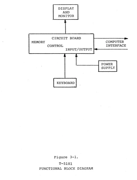
DISPLAY AND HONITOR
CIRCUIT BOARD
CONTROL
-
--COMPUTER INTERFACE
INPUT/OUTPUT~---KEYBOARD
Figure 3-1.
T-SIOl
[image:43.613.77.521.125.707.2]w
'I
w
OPERATOR'S QUICK REFERENCE GUIDE
CONTROL
FUNCTION SEQUENCE ASCII CURSOR ~ CTRL I H Xor Y CODE CURSOR l CTRL/J 1 SPACE CURSOR t CTRL I K 2 ! CURSOR -+ CTRLI L 3
..
HOME CTRL/ /I. 4 #
SKIP CTRL II 5 $
NEW LINE CTRL/- 6 %
7 & ·PROTECT ON ESC &
·PROTECT OFF ESC , START WRITE PROTECT ESC END WRITE PROTECT ESC CLEAR ALL TO UNPROTECT SP ESC + SEND LINE UNPROTECT ESC 4
SEND PAGE UNPROTECT ESC 5
8
9 (
10 )
11 •
12 +
13 ,
SEND LINE PROTECT ESC 6 14
-SEND PAGE PROTECT ESC 7 15
CLEAR ALL TO NULL ESC * 16 I
CLEAR PG TO NULL ESC 17 0 CLEAR PG TO SPACE ESC ,
KEYBOARD ENABLE ESC
..
KEYBOARD DISABLE ESC#
LOAD CURSOR ESC READ CURSOR ESC ?ADM·' MODE ON ESC %
18 1
19 2
20 3
21 4
22 5
ADM·' MODE OFF ESC $ 23 6 CHAR INSERT ESC Q 24 7
CHAR DELETE ESC W 25 8
LINE INSERT ESC E
LINE DELETE ESC R LINE ERASE ESC T
26 9
27 :
ERASE PAGE ESC Y
PARTIAL SEND ESC S TRANSMIT Y, THEN X. BACK TAB ESC I BACK PAGE
START/END BLINK FIELD ESC
"
FORWARD PAGESTART/END BLANK FIELD ESC
-
* SET PAGE EDIT ·SET BLOCK MODE ESC B CLEAR PAGE EDIT ·SET CONVERSATION MODE ESC C PRINT PAGEUNFORMAT PRINT PAGE * Use available key rather than escape sequence SET PROGRAM MODE when making a keyboard entry. (PROT MODE, CLEAR PROGRAM MODE PAGE EDIT, CONV MODE) SET COLUMN TAB
ABSOLUTE CURSOR POSITIONING
-ASCII ASCii Xor Y CODE X or Y CODE
28 55 V
29 ( 56 W
30 = 57 X
31 ) 58 y
32 7 59 Z
33 @ 60 I
34 A 61 \
35 B
I
36 C
37 D
38 E
I
39 F
62 I
63 1\
64 65
66 d
40 G 67 b
41 H 68 c
42 I 69 d
43 J 70 f'
44 K 71
45 L 72 9
46 M 73 h
47 N 74
48 0 75 I
49 P
I
50 Q
76 k
77
51 R 78 m
52 S 79 n
53 T 80 0
54 U
.. ---- --_ ..• "-_._-ESC I ERASE LINE TO NULL ESC t
ESC K ERASE PAGE TO NULL ESC y
ESC N SET STATUS 1 ESC t.:. ESC 0 CLEAR STATUS 1 ESC h
ESC P SET STATUS 2 ESC e ESC p CLEAR STATUS 2 ESC t ~
ESC U SET STATUS:3 ESC 9
ESC X CLEAR STATUS 3 ESC f
ESC V SET STATUS 4 ESC < CLEAR STATUS 4 ESC >
I
•
0-~~. lit .. •"
•• • • ••• • ••• .. ~& • • • •
..
• • H"" " "
. ·
e • •• e.
..
• •..
• • •"
.
...
"...
".. ..
••••
....
••• • •.
...
II .... •..
"fl< • • • • •..
c..
..
" .fI>a.e •
.,.
..
..
$"
..
•• •••
• •..
.00100..
....
• • .C a co..
• ••
• • ••••
...
..
• to • • •"
....
'" ~
..
"
....
,.. .c •• o .lVeeo OCiioe. 0 • • 0 6 .<'$c,;,o Gl 0'. tt'e • •••• -v .... • •••• tt(lC'jo: f18 c_-. "" •. .. • • 'IJo'&• • • 0 _ •
• • It
•••
•
••
••
• e •..
..
"
• • ceo ..... ..
•...
&tOUl •" •
•
•• ••
•
•
•..
•.,
• •
..
• •..
..
..
..
•....
e..
• • Q •..
.. ..
•..
" • •.. ..
• •"
.. ..
..
• •..
...
..
.. ..
" c'"~.: •••
..
..
•
..
oalil." • • • t:
..
•..
..
..
•..
• •• •..
..
"
..
...
at'. •••••
0 ••..
•..
• • • •••••..
" • c.~o • .,eflt',iI(tc
•••••
•
••••
•••••
co •••..0 ..
... 0.
000 • • • • • • • &' • • • 86 e"e.r •• • •••• •• (t.~ • •••• 5.:. Iii • • • •• eG a-&Qtl!• •
..
..
• • •• • • •..
• • •• • • " • ".9. o. •
..
•..
..
..
• "..
" "• •
..
eC ••••
..
..
•
• • •..
..,.
•..
• • •
....
• • • • • "6~ • • 0.t.,1IO •• ••••• 0
..
• • • •..
• • •• t>..
• • •••• •
••
• •..
• • .,. • Il •..
• • •
•
•••
••
• •..
•
• • "•••
• O~. ee: ••"
• ••••••
. ..
.,.
.e.
•••
..
..
'.6
·
•
.-
•
..
to...
• ••
•..
•"
..
..
..
••
••
..
•
..
.. ..
•• "e •..
• • • • • • ••••
0..
·
....
"
• • •..
• •• ••..
o •• a •.. ..
•
..
.. ..
•
•••
• •..
•••
&..jjjt.
..
•..
..
.$ •..
..
..
..
•
•••
•
"eo.•
..
..
"'..
• • • •• • • •....
."•
•••
..
• • ••••
•
••
•
• •..
•..
••
•
....
• •••• •• e ••••...
•••••••••
• "...
..
••
..
..
..
"..
.c .
• •
..
..
..
• r·" •
..
0 •"
..
.,"
..
..
•..
....
,,.. ~.
e..
••
....
0> «..
"
..
• • • •..
•
..
•.. ..
• • " •..
"" •..
••
.. ..
..
..
.ae:6..
..
• .eGa••••
• •••••••
• " •• "..
"..
..
•..
" ••
....
O • • CS!ft •.. ..
• ••
" • " • • •..
e..
..
• • • •• • •..
.. .. ..
• • • • •..
".. .. ..
•"
•.. ..
•..
.. .. ..
•• • •••••
• • • • G •....
••••
••••• • ••••
• ••••••
•..
••••• • " • •."
.
••••
••• ••••
"..
00 • • •'.
•
•
•..
•
•
• • ••••••
..a., • ..~o•
..
•
•
~, •..
•
•..
•
..
•
"
•..
..
•..
• " .."
GC •..
II..
•
•
•
•
• • •..
•
• ••
• • • • •• 0 .o. • "• • • 0 • 0 •• oe
•••
•..
•..
•
.. ..
..
..
•..
eo..
...
0 ••
•
..
..
e•
••
•• •
•
..
..
..
•
•..
•...
• •••
•'"
..
•
0..
•
••
•
..
••
••
..
• • •..
- • •••
••
••
•
•••
•
•
••
••
••
• • ••••• • • 00 • •••• •••••• •
•
•
• • • • • • • ••
• • •• ••
".
~ • • ttO •.
....
..
•••..
..
• • ••..
•....
..
.,• 0 ; 0 .
..
....
•" • • • •••• • • •
..
• " • r...
• " •....
• •..
•
• • ~.oe • •• e..
..
•..
•
..
..
"
..
.. ..
..
•..
"•
"
• •..
•..
1\•
•
..
• 0 •• ••
•.. .. ..
r,.. ..
" C>••••
',Ie •• •••• .~..
•••
..
••••
•
• e~. • • •..
..
•"
..
•..
..
...
..
• ••••
•..
..
• • ••• eo...
••• • 0••
..,...
•••
• • 0 ••
•
..
••
•
• • • • ••••••
• • • ••••• " • •
...
.
...
•
• ••
..
• • • • • • • •..
• ••• it "t~ Q ('4•
•
..
• •..
•• •
•..
• ••
..
..
II • • • 0 .CI~t#O~"'
..
"....
•
0••
0•
• • ••
••••
• ••
• • . 0..
•
..
• • • V~•
..
•
••
• ••
••
• • • •..
• •••• • • •• e.
...
•
• [image:45.615.49.576.64.657.2]The standard display character set for the T-5101 is 96 characters
ASCII. Control characters (32) can be displayed if: 1) preceded
in transmission from computer or keyboard by ASCII ESC U code
sequence or, 2) if terminal status is set to program mode.
Reverse image display is used if the cursor is positioned over data.
Selected fields on the T-5101 display may be 1) caused to blink at 4
images/second, 2) protected from overwriting, characters of which are displayed with reduced intensity or 3) blanked by inhibiting the display of character stored in terminal memory locations
cor-responding to security fields. In addition, eight status indicators
are displayable on the right of the screen, each as a full 14 x 9
dot block.
A complete page of characters in the T-5101 contains 24 character lines, each with 80 character positions, providing a total display
capacity of 1920 characters per page. Display fields are refreshed
at a rate set by a crystal oscillator synchronously with 60 Hz input
power in the standard terminal. This rapid refresh rate generates
flicker-free images and high contrast display even in bright ambient light.
vertical and horizontal beam deflections for the display are generated by trigger signals derived from the T-5101 system clock and logic input
to the monitor. The CRT monitor is a solid-state unit designed for
reliability and high quality reproduction in industrial and commercial
installations. The theory of operations of the monitor is detailed
in Section IV of this reference manual.
MAIN CIRCUIT BOARD
All of the T-5101 terminal control functions are incorporated in a single printed circuit board mounted directly beneath the CRT display
tube. Using a single circuit board eliminates interconnections and
cabling, and increases terminal reliability. The board contains the
microcontroller, display memory logic electronics, transmission rate
control and data interface electronics. Discussion of the functions
of the main circuit board is given in detail in Section III of this
manuell.
POWER SUPPL J'
The T-5101 main logic board is supplied with 5 volts D.C. from a
sepa-rate power supply module. The T-5101 D.C. power supply is rated at
12 amps and is equipped with its own solid state voltage regulator
and current limiter. Line and load regulation of .075% assures stable D.C. power availability for all T-SlOl display terminal functions.
KEYBOARD
Your T-S10l terminal is equipped with a standard 118 key keyboard,
capable uf being located remotely up to
sn
from the T-S10l displayunit. Keys are positioned on 3/4" centers with 3/8" offset needing
2 oz. operating force, and have two key rollover feature such that if a key is depressed before a previously operated key is released, the second key code is transmitted upon release of the first key. The T-S10l Keyboard layout is depicted in Figure 3-3.
Normal Keyboard Operation
Single keystrokes or certain simultaneous multiple keystrokes are encoded into ASCII seven bit binary codes which are either stored in memory, displayed, and/or transmitted to the data interface
depending upon the transmission or program mode of the T-S10l. ASCII
Control characters can be entered into memory and displayed on the
screen while the terminal is in program mode. Terminal functions
and keys used are given in Table 3-1.
The T-S10l standard keyboard encodes 96 ASCII charac:ers for
trans-mission and display, As an option, the T-S10l keyboard can be equipped
to encode lower case alphabetic characters and the special characters
{ I } , I ~ for display.
The T-S10l keyboard can be enabled and disabled locally and remotely by computer control using the following sequence of keystrokes or equivalent ASCII codes:
ESC q disables all keyboard functions except RESET
ESC" enables the keyboard and restores keyb8ard control.
Since ESC # sequence may be accidentally initiated manually, the
keyboard may need to be unlocked by depressing the RESET key.
SHIFT LOCK Key provides a lock of the shift function that
is cleared by operation of either shift key.
The "locked" shift does not perform the shift operation on the special function keys, PRINT key, SEND keys, CLEAR keys, EDIT keys or
(
Table 3-1. KEYBOARD OPERATIONS
Operation
A ~ CHARACTER DISPLAY
1. Alphabetic Upper Case
2. Alphabetic Lower Case
(Optional with SHIFT)
3. Numeric
4. Special Characters
5. Special Characters with
6.
SHIFT
Special Characters with CTRL or CTRL/SHIFT
ASCII CODE
NULL SOH STX ETX EOT ENQ ACK BEEP BS HT LF VT FF CR SO SI DLE DCI DC2 DC3 DC4 NAK DISPLAYED CHARACTER A .t' ~ D E F .Q.
-'-a
~. ~o
I 2 3 4 UKeys Used
A to Z
A to Z
o
to 9 Main Keyboard orNumeric Pad
- . @ - []
;J\',./
II # $
%
&( ) *
=I
.
KEYS USED
CTRL/A
SHIFT/SOM-EOM, CTRL/B SOM-EOM, CTRL/C
CTRL/D CTRL/E CTRL/F CTRL/G
- , CTRL/H TAB,CTRL/I
LF, l, CTRL/J
t I CTRLjI<:
- , CTRL/L
RETURN, CR, CTRL/M
Table 3-1. KEYBOARD OPERATIONS (Continued)
DISPLAYED
ASCII CODE CHARACTER KEYS USED
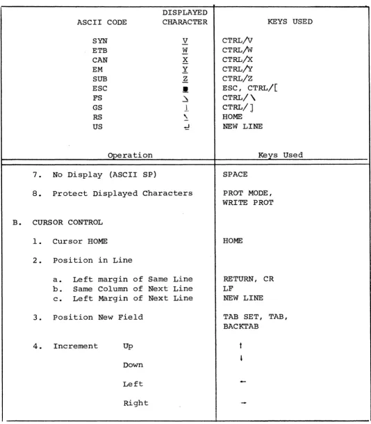
SYN V CTRL/V
ETB
-
w
CTRL/WCAN X CTRL/X
EM Y CTRL/y
SUB £ CTRL/Z
ESC
..
ESC, CTRL/[FS '\ CTRL/\
GS
1
CTRL/]RS
,
HOMEUS ~ NEW LINE
Operation Kevs Used
7. No Display (ASCII SP) SPACE
8. Protect Displayed Characters PROT MODE,
WRITE PROT
B. CURSOR CONTROL
1. Cursor HOME HOME
2. position in Line
a. Left margin of Same Line RETURN, CR
b. Same Column of Next Line LF
c. Left Margin of Next Line NEW LINE
3. position New Field TAB SET, TAB,
BACKTAB
4. Increment Up t
•
Down
Left
-Right
[image:50.613.44.578.66.676.2].Table 3-1. KEYBOARD OPERATIONS (Continued)
C ..
Operation
TERMINAL CONTROL
1. Reset
2. Break
3. Clear Screen or Foreground to:
a. Spaces
b. Null Codes
4. Audible Tone
5. Display Extended Memory
Control (Optional)
D. DATA TRANSMISSION CONTROL
1. Transmission Mode
2. Transmission Initiation
(block mode)
3. Send to Printer
4. Transmitted Text Delimiters
5. Special Functions
Keys Used
RESET
BREAK
CLEAR SP CLEAR NUL
CTRL/G
PAGE FWD. PAGE BACK
BLOCK MODE. CONV MODE
SEND LINE. SEND MESSAGE. SEND PAGE
SOM - EOM
w I I-' I-'
BITS BITS
4321 765
CONTROL
o
000 001
2
GRAPHIC CHARACTER SET
3 4 5 6' 7'
010 011 100 101 110 111
BINARY CODES
2 3
010 011
ESCAPE SEQUENCE
4 5
100 101
I P I PRINT
6
Ip1 UNFOR~'AT ~ PRINT
0000 NUL OLE
f . - - - -f--- --- --f-- .--- .---- ---- - ---+---+----il--- --. SP (/) @ P --+-"--+..---L---+-.---+---.---+---'----t---i P ~ PAGE
0001
--+-~~-
DCI I 1 A D---f--. \___
-0010 i. S~~ ___ _ 1---_00_1_1
+--~l~TX
__ _
0100 1---0101 0110 EOT END ACK
f--~--l~--I
-DC2 " 2 B R
. t
-DC3 ~ 3 C S
- - - f---I---
----DC4 S 4 D T
- - - -- - - - , -
-q
b
d
~~~~: -~t:
t-
t~:
C:
I----:-:-:-:+---l-.-:~-;-,:-:, ~ ::~~=-
I'f
~:~~:
:
wee"",,,
W"'A>"
:
~m ~--~~I~r~~;:~=+::N~~~~~L~A~~~C~A~L~E-R=-A:-L=L=:W=-,:~N-~::=~~~-C=~-E~R=-F:G:::::::;::;;::::::::::::::::::::~---+---~
1 - - - + - - - 1 - - - 1 - - - -~ .--.. -- l f +
-< I < I STATUS 4 1100
(-»
FF FS L \ I i--="-ION
I---+----I---I---I--'---t--- ---- ---- ---
I "I LOAD1101 CR
1110 SO
1111 SI
"DISPLAYED AS UPPER CASE GS
(HOME)
RS (NEW L1NEI US
- ~ M
> N
/ 7 0
J m } f---J CURSOR
--~-