MARCH'f974
Centrdriics No. 3740?OOO Rev.A,
RS232
INTERFACE
. TECHNICAL
MANUAL
I: E nTRO nil: S
" data computer corp.
THE INFORMATION CONTAINED HEREIN IS PROPRIETARY AND IS NOT TO BE RELEASED
OR REPRODUCED WITHOUT WRITTEN PER-MISSION OF CENTRON1CS data computer corp.
I:EnTRDnll:S
CENTRONICS DATA COMPUTER CORP.
HUDSON. N.H. 03051
TELEPHONE (603) 883e0111
EASTERN REGION: (617) 272·8545 (MASS.) CENTRAL REGION: (513) 29~070 (OHIO) WESTERN REGION: (714) 919-6650 CALIF.)
CENTRONICS DATA COMPUTER, LTD. (CANADA)
MISSISSAUGA. ONTARIO (416) 625.Q770
CENTRONICS DATA COMPUTER CORP. LTC. (U.K.)
CHEAM. SURREY (01) 643-0821n
CENTRONICS DATA COMPUTER CORP. (GMBH) GERMANY . 6 FRANKFURT/MAIN 66332112
CCopyrfght 1975 Cen1tonlq .. ~·~, Corp.
AJI rIshU rwtIf'I'IId .~. ~.~ ,I . . ~
PI1enU pend1ng In USA ~~~f.~
TABLE OF CONTENTS
1. General. · · · • . · .2. Physical Description
3., Programmi ng Notes · • ·
.:4~ Installation • • • · ·
5. Board Configurations. ·
6. Data F.1ow· • • • • • •
7~ . Theory of Operation ·
8 ... Schematic and Assembly Drawings • • • • ·
9.:: I nterface Connector. · • • • •
10-:. Glossary • · • · · · · • • • • • •
~i'gure 1
Fi,g~,re 2
Fig~lre 3
Figure 4
fi~gure 5
Figure 6
F.igure 7
Figure 8
Figure 9
Figure 10
'F1~ur~' 11
!~·'9'Ure 12
)":'1010«:; .
rigure 13 Figure'14 Ftgllre 15
III u'strati ons
RS232 Interface Data Flow Diagram RS232 Interface Installation Diagram. Serial Input Data •.
Serial Input Timing · • Parallel Output Data · · Parallel Output Timing •
Schematic Diagram (Sheet 1)~ • • • • •
Schematic Diagram (Sheet 2). Schematic Diagram (Sheet 3).
Schematic Diagram (Sheet
4).
Schematic Diagram (Sheet 5) • .
Electronics Cavity Assembly . . . Component Board Assembly (Sheet 1) •
Component Board A~semb1y (Sheet 2) •
Cable Assembly (W4) . • • . . . ·
Page
• 1
· . . 1
• • 3
• • • • • 4
• • 6
· 8 • • 9
• 18
• • • • 29
. • . . 30
• • 2
• • 5
• • 10
. . . 12
• • • 14
• 15 • • • 19
• 20
. . .
.
• • 21
• • 22.
23 24
• . • 25 . . . 27
1. GENERAL
The RS232 Interface is designed primarily to interface the 202C or 2020 Dataphone directly (or indirectly via an optional Ring Buffer*) to the Centronics Models 101, lOlA, 102A or 306 printers.
The interface accepts serial input data from the data set, assembles the received data into 8-bit characters (seven data bits and one parity bit), checks the parity of the received data and transfers the assembled character in paral,lel to the printer. Signal levels between the interface and the data set conform to RS232 standards. Signal levels between the interface and printer are TTL compatible.
A reverse channel indication to the data set, controlled by the received data (EOM code) and the status of the printer (or optional Ring Buffer), prohibits data transmission whenever the printer (or Ring Buffer) is not able to accept new data. The absence of a reverse channel response ,·to a data transmi ss i on i ndi cates that a pari ty error was detected in the
received data.
A simplified block diagram of the major signal flow between the
data set, RS232 Interface, and Printer (or Ring Buffer) is shown in Figure 1.
2. PHYSICAL DESCRIPTION
The RS232 Interface consists of a single printed circuit board a~d
cable assembly all contained in the printer enclosure. The PC 'board plugs into the interface slot at the rear of the printer. The cable assembly consists of a 10-foot cable with a small etched card (fingerboard.) connector at one end and a 25-pin cinch type DB-106040432 plug at the other end. The fingerboard plugs into a connector on the right side of the interface card, and the 25-pin connector plugs into the data set. A connector plate and strain relief bushing is also included which allows the cable to attachpto the speaker bracket at the rear of the.printer.
I N
I DATA
SET
OSC
.2 or 1.0 ___ BAUD COUNTER
STROBE
MHz
RECEIVE DATA (BB) DATA SET READY (CC) CARRIER DETECT
(CF) t - - - L _ _
I
y
(!lLaJ
0::::
t:: ... :J: Vl
...-_ _ _ D_A_TA__.(8_B-IT-S.;..)
----I
r-->
.7
1 I MODELSSOM/EOM
I
I
+5V DECODE
I I
/ ' ,,0
(CD) - DATA TERMINAL~I--_ _ --c::-)l:.",~~",,_;:)-_S_E_LE_C_T _ _ _ _ _ _ _ _ _ _ -+-_ _ _ _ _ _
1_1 __
-1101, lOlA, 102A or 306
PRINTER
- READY - " " - I I
"" EOM & NO PARITY I I
REVERSE _ ACTIVATE ""i /'''' ERROR I I /\
CHANNEL ~ ~
LOGIC - REV. CH. ' ' 0 - _ _ ~ 253 CHARACTERS _ _ _
1_1 __
-r
--LL-,
·~EXTEND
. IL~
I
REV. CH. L_-../! OPTIONAL
I
n.
I
RINGI
" ').. BUSY BUFFER
~
. '" 2: 229 CHARACTERSI
I
L _ _ _ " .---~. --":-:~--' - '
- - - L __
.J
(SA)"",,! REVERSE CHANNEL
3. PROGRAMMING NOTES
3.1 CONTROL CHARACTER FOLLOWED BY EOM\~
When the RS232 Interface is used, any transmitted control character which could cause a busy condition (e.g., LF, FF, CR, etc.) must be
immediately followed by an EOM. The reason for this is a BUSY signal from the printer does not activate Reverse Channel, but only extends Reverse Chan,n.el, if it was previously activated.
Without a Reverse Channel response, the data set receives no
indi-cati~n
that the printer has gone busy and further data transmissions could!
resJlt in a loss of data.
An EOM (with no parity errors in the preceeding message) will activate Reverse Channel.
In the 102A, a busy condition can also be caused by an Elongated Character code (octal 016), because the carriage must return to the left
margin before printing elongated characters. As a ~esultt in a 102A an
RS232 Interface, each octal 016 code must also be followed by an EOM.
3.2 . TRANSMISSION DELAY
The Reverse Channel signal to the data set is at least 200 milli-seconds· long and remain's active as long as the printer (or Ring Buffer) busy condition exists. After going inactive, Reverse Channel cannot be
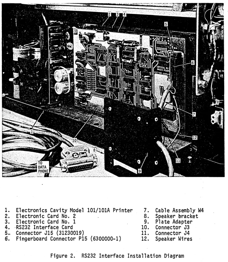
4. INSTALLATION
The RS232 interface is installed in the Model 101, lOlA, or 102A
printer, as follows: (Reference: Figure
2)
1. Remove the 36-pin Amphenol connector (57-40360) from the speaker bracket at the rear of the printer. Retain the hardware.
2. Unsolder and remove the two wires from the speaker.
3. Remove the ground connection near the speaker bracket and reta in th.e .. hardware.
4. Unplug the fingerboard from connector J4 and remove the entir.~·,
W2 cable, finge~board and amphenol connector. Retain the
hardware for possible future re-conversion to parallel interf~fe.
. 5. Plug the RS232 interface board into connectors J3 and J4 at the rear of the printer.
6. Plug the fingerboard from the RS232 cable assembly into con-nector J15 on the interface card.
7. With the hardware retained from removing the Amphenol connector
. , .
(Step 1)~ secure the adapter plate attached to the RS232 cabl~
assembly, to the speaker bracket.
8. Solder the two loose wires located on the fingerboard to the speaker.
9. Plug the other end of the cable assembly to the data set.
To install the RS232 interface, a 306 printer, refer to Field
1. Electronics Cavity Model 10l/l01A Printer 7. Cable Assembly W4
2. Electronic Card No. 2 8. Speaker bracket
3. Electronic Card No. 1 9. Plate Adapter
4. ·RS2j2 Interface Card 10. Connector J3
5 •. Connector J15 (3l2300l9) 11. Connector J4
6. Fingerboard Connector P1S (6300000-l) 12. Speaker ~Jires
5. BOARD CONFIGURATIONS
5.1 GENERAL
Each board ;s stamped with its baud rate followed by a dash number and/ or a special number.
For example,
1. 2400-2: The 2400 signifies that the board is configured for a 2400 baud data input, the -2 specifies the jumper connections on the board, as shown in Tables 1 and 2·in this section .
. 2. 1200-3-S7 signifies a special board configured for 1200 baud and the -3 jumper connections specified in Tables 1 and 2, but with special modifications such as a component change on the board or a cut_ in the etch. Each special is described in a separate documentation package.
5.2 BAUD RATE
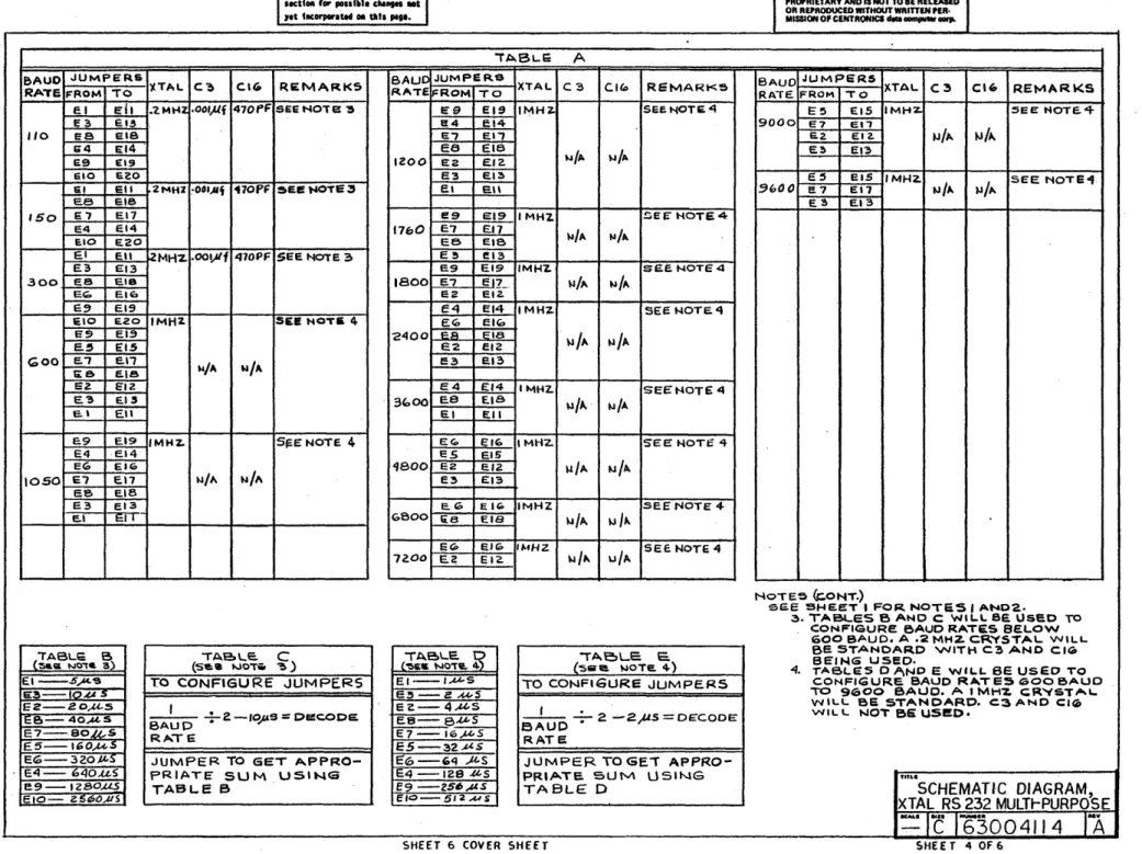
Baud rates ranging from 110 to 9600 can be accomodated by the RS232 interface. For rates below 600 baud, the oscillator circuit contains a 0.2 MHz crystal and capacitors C3, C4 and C16. For rates of 600 to 9600 baud, a IMHz crystal is used and capacitors C3, C4 and CI6 are deleted.
The crystal and jumper configuration for each baud rate is specified· in Tables A through Eon drawing #63004114 (sheet 4).
As ~n example, the jumper connections for a 9000 baud rate are as
follows:
1. Referring to Table A and Note 4, a 1MHz crystal is used, C3, C4.: ~
and C16 are not used, and Tables D and E specify the jumper con~ections ..
5.3 JUMPER OPTIONS
E5-E15 (32 usec) E7-E17 (16 usec) E2-E12 ( 4 usec) E3-E13 ( 2 usec)
54 usec (total)
There are presently five dash numbers specifying standard jumper options. These dash numbers and options are listed in Tables 1 and 2 in thJs
Table 1
Jumper Configuration
DASH JUMPER OPTIONS
NO. (see Table 2) REMARKS
-1 A, F, I, J, L, N Direct Input to Printer (Even Parity)
-2 Bt F, It J, L, N Direct Input to Printer Input (Odd Parity)
-3 A, G, H, K, L, N Ring Buffer Input (Even Parity)
-4 B, G, H, K, L, N Ring Buffer Input (Odd Parit~)
-5 0, F, I, L, N, P Reference S3 Special
See also Tables A through E on Assembly and Schematic Drawings
JUMPER OPTION
A B
C
o
E F
G
H
I
K
L
M
Table 2 Jumper Options
JUMPER CONNECTION
E22 to E21, E25 to E26 E22 to E23, E25 to E26 E22 to E24" E25 to E24
E22 toE21, E25 to E24
E22 to E23, E25 to E24
E28 to E27 E28 to E29 E32 to E31 E32 to E30
-
E"~5";~ ~-~~
E35 to E34
E36 to E37
DESCRIPTION
Even Parity (Normal) Odd Parity (Normal)
Parity Disable (Disable Presetting of
@ Sign). '
Even Parity @ only (Disable Parity but
Print @ Per Character).
Odd Parity @ only (Disable Parity but
Print @ Per Character).
'Busy Enable (Normal)
Busy Disable (Ring Buffer) HICNT Enable (Ring Buffe'r)
HINCT Disable (Normal) Enables Reverse Channel when HICNT is not used.
Select In (When selected, CD is held at +12V) •
Select Out (CD is always held at +12V) (Ring Buffer).
Protective Ground In
Protective Ground Floating
N E39 to E38 Reverse Channel Normal Output
o
r
E40 to E35 CD (Controlled b.y Busy, Normally -12V~~
' when active +12V).P <f E41 to E35 ~.:S~CD (Controlled b.y Busy Normally +12Y<~
6. DATA FLOW
6.1 DATA TRANSMISSION BY DATA SET
Once the call has been established, either manually or with the automatic calling unit, the transmitter starts data transmission with a Start of Message code (SOM, Octal 001). This must precede every transmitted line of data and every command code.
The data is transmitted serially and consists of one start bit, seven data bits, one parity bit, and one or more stop bits. In the 101, lOlA or 306, if a short line is to be printed, the line is terminated
with a Carriage Return code (Octal 015). After the carriage return or control function is transmitted, an End of Message (EOM, Octal 003) is transmitted.
The transmitter must then wait for the Reverse Channel to go active indicating an acknowledge from the interface. If the Reverse Channel level is not received by the transmitter within four seconds after EOM has been transmitted, a parity error may be assumed and the line or function may be retransmitted. If the Reverse Channel level is received, the transmitter
waits until, the Reverse Channel line goes inactive, waits at least 200 milliseconds, and then transmits the next line of data.
When all data has been transmitted, the call is terminated in accordance,with the 202D'Dataphone procedures.
6.2 DATA RECEPTION BY THE INTERFACE
Once the call has been properly established, the received SOM character' clears the interface logic.
The leading edge of each Start bit starts a clock which clocks each sub-sequent bit from the data set into an 8-bit shift register. Once the shift register is loaded, parity is checked. If parity is correct, the character in the shift register is transferred in parallel to the printer (or Ring Buffer).
If parity error is detected, an octal 100 (@ sign) is forced into the shift
register, prior to transferring the data.
Data reception continues in this fashion until an EOM code is
received, at which time the parity flip-flop is checked. If no parity error was detected, Reverse Channel is activated and remains active until the
~~ ~
7. THEORY OF OPERATION
This Theory of Operation section describes the detailed operation
of the RS232 Interface. Throughout this section, ~eferenceis made to
the schematic diagrams in Section 8. The section is subdivided into the following major categories:
7.1 Power-Up Prime 7.2 Interface Levels 7.3 Serial Data Input
7.4 Parallel Data Output (to Printer) 7.5 Status Indication
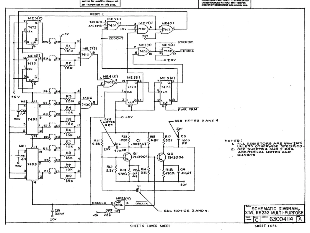
7.1 POWER-UP PRIME
Resistor R28 and capacitor C17 from the power-up reset (prime) circuit. With C17 initially uncharged, OV appears at PWPPRM when power
is first turned on. This resets ~haracter Clear flip-flop CHACLR
(ME14(l»* which resets flip-flop ME8(2) and triggers one-shot ME19(2) generating a 200 millisecond pulse which resets latch flip-flop ME4(3) and
(4). Signal PWRPRM also resets the ODDCNT flip-flop ME5(2), to initialize the STROBE logic.
7.2 INTERFACE LEVELS
7.2.1 Inputs
The signal leveis from the data set to the RS232 interface board (+12V and -12V) are converted to TTL levels (OV and +5V respectively) by
el~ment ME22 (Type MC1489L). The 6.8K resistors (R21, R22 and R23) in conjunction with the 470 pf capacitors (CS, C6 and C7) establish proper hysteresis levels and frequency response for the circuits.
7.2.2 Outputs
The signal levels from the interface board (OV and +5V) to the data set are converted to +12V and -12V levels respectively by element ME26
(Type MC1488L).
When the printer is selected, pin MEIB-4 is held low which holds the DATA TERMINAL READY signal (CO) high. The Request to Send signal (CA) is constantly held low by +5V at the ME26 (3) input.
7.3 SERIAL DATA INPUT
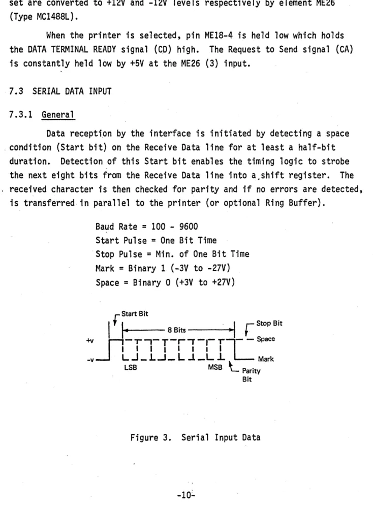
7.3.1 General
Data recepti.on by the interface is initiated by detecting a space _ condition (Start bit) on the Receive Data line for at least a half-bit
duration. Detection of this Start bit enables the timing logic to strobe the next eight bits from the Receive Data line into a,shift register. The . received character is then checked for parity and if no errors are detected,
is transferred in parallel to the printer (or optional Ring Buffer).
Baud Rate
=
100 - 9600Start Pulse
=
One Bit TimeStop Pulse
=
Min. of One Bit TimeMark
=
Binary 1 (-3V to -27V)Space
=
Binary 0 (+3V to +27V)rStart Bit
I
'I.
~ 8 Bits.
. I
•r
Stop Bit+vjl-"-T-"",.-t-r.l
SpaceI I I I I I I I
-v L...J _ L...l_ L...L _L l Mark
LSB MSB
L
ParityBit
7.3.2 Shift Register
Serial data is assembled in an a-bit shift register ME25. The data input to this register can be in either serial or parallel form depending on the status of the Shift/Load control input (pin 23). A high LOAD signal enables the serial input (pins 1 and 2) and a low LOAD enables the parallel inputs (A through H). Serial data is shifted
synchronously on the positive-going clock input (pin 13). Data is shifted in the direction of A to H. Parallel input data is loaded int'o the
associated flip-flop and appears at the outputs on the positive-going clock input.
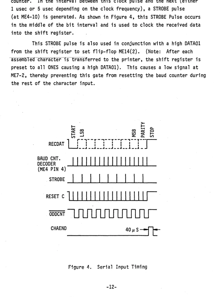
7.3.3 Input Timing
The input timing logic for the RS232 interface is contained mainly on sheet 1 of the schematic diagrams. With no data being received, the Baud Counter (elements MEl, ME2 and ME3) is held reset by a high output from ME7-6.
As soon as the Receive Data line changes to a Space condition (+12V), RECDAT goes low. If at this time, the data set is ready (DSTRDY is low) and a data carrier is present (DACADE is low), the output of
ME12-3 goes low. This causes a high out of ME7-12 and a low out of ME7-6, enabling the baud counter.
The crystal oscillator output OSCCLK (either .2MHz or 1MHz depending on selected baud rate) is counted down by the 10-stage Baud Counter. Each stage in the counter successively halves the output frequency of the
preceeding stage. As a result, for a .2MHz clock frequency, the E1 output remains high for a 5 usec interval and the 10th stage output E10 remains
high for a 2560 usec interval. For a 1MHz clock frequency, E1 is high for
1 usec and E10 is high for 512 usec.
When the desired count is reached,* decoder outputs ME7-8 and ME6-8 both go low causing ME4-4 and the J-input to ME5(1) to go high.
The next clock pulse sets flip-flop ME5(1). This causes a low input to ME7-4 and a high output at ME7-6, resetting and disabling the baud rate counter. In the interval between this clock pulse and the next (either 1 usec or 5 usec depending on the clock frequency), a STROBE pulse
(at ME4-10) is generated. As shown in Figure 4, this STROBE Pulse occurs in the middle of the bit interval and is used to clock the received data into the shift register.
This STROBE pulse is also used in conjunction with a high DATA01 from the shift register to set flip-flop ME14(2). (Note: After each assemJ51eacnaracter is transferred to the printer, the shift register is preset to all ONES causing a high DATA01). This causes a low signal at ME7-2, thereby preventing this gate from resetting the baud counter during the rest of the character input.
>-~ ~ ~
0:: ~ ~ ~ 0
~ ~ ~ ~ ~
~ ~ ~ ~ ~
RECDAT
ur-l--r-l--r--r-l--1---r-__ .I ur-l--r-l--r--r-l--1---r-__ .J. __ .I __ ..I • • .1 __ .J. __ .J. _
J
BAUD CNT. DECODER
(ME4 PIN 4)
I1IIII111111111111
. STROBE -'---____
I ____
1 _____
1 ...
1
...&.I~I ~I--,I_
RESET C
11 I I II I I
,I III IIII I I
ODDCNT
CHAEND _ _ _ _ _ _ _ _ _
With the counter reset, flip-flop MES(l) is reset by the next low-going OSCCLK. The low low-going MES-12 output then toggles the ODDCNT flip-flop set. This prevents the next decode output from generating a STROBE pulse, and allows only every other decode output to generate a STROBE. This is necessary since the counter is enabled on the leading edge of the Start bit and the decode pulse occurs at twice the baud rate. As a result, the first decode pulse develops a STROBE in the middle of the first bit interval. The second decDde pulse which occurs at the end of the first bit interval,
is blocked by flip-flop MES(2) - ODDCNT. The third decode pulse is then enabled, the fourth blocked, etc., causing all STROBES to occur in the" middle of the bit interval.
The first STROBE pulse loads the Start bit in the shift register. After the ei ghth STROBE pul se, thi s Start bi t appears at the "DATA01 output. The ninth STROBE pulse then shifts the parity bit in.to the register and resets flip-flop ME14(2) since DATA01 is now low.
With signal ODDCNT low, the·baud counter counts through one more" cycle before being reset by ME7(1). However, no more STROBE pulses are" generated until the next Start bit is detected.
7.3.4 End of Character
The STROBE pulse that shifts the parity bit into the shift register also resets flip-flop ME14(2). This allows the next high-going ODDCNTout-put to set flip-flop ME8(2).Tosynchronize the received character with the. internal timing in the printer, the next high-going oscillator output from the printer (OSCXT) sets the End of Character flip-flop (CHAEND). Signal
CHAEND initiates the parallel transfer of the received character to the printer.
When the parallel transfer is accomplished, CHACLR goes low resetting flip-flop ME8(2) which allows' the "next OSCXT pulse to reset flip-flop
7.3.5 Parity Check
The parity circuit consists of flip-flops (ME9(l) and ME9(2). While data is being shifted into the shift register, the STROBE pulse toggles flip-flop ME9(l) whenever RECDAT is high (ONE). As a result, at the end of the character, if the character contains an odd number of ONES, ME9(1) will be in the set state. If the character contains an even number of ONES, ME9(l) will be in the reset state.
By jumper option, even or odd parity (CHAPAR) can be presented at the input to flip-flop ME9(2). The jumper connection is such that CHAPAR should be high if a parity error is present (see Section 5). If a parity error is present, flip-flop -ME9f2) is set by signal l'ARCK and remains set ·until the next SOM character is received.
Also, if a parity error is detected, an octal 100 (@ sign) is preset
into the shift register by gate ME11(3) before transferring data to the printer.
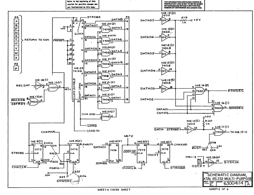
7.4 PARALLEL DATA OUTPUT (to PRINTER)
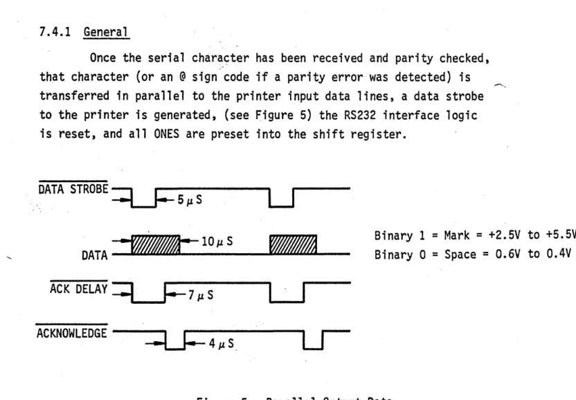
7.4.1 General
Once the serial chara9ter has been received and parity checked,
that character (or an @ Sign-code if a parity error was detected) is
transferred in parallel to the printer input data lines, a data strobe to the printer is generated, (see Figure 5) the RS232 interface logic is reset, and all ONES are preset into the shift register.
DATA STROBE
==l..Y=
. 5~S
u
DATA
_1
.... ""-..-:"""'"""'"-··
_lO_J1._S_--.&o~"""""'"""""'-A
_ _ACKNOWLEDGE --~---. 1_
~4J1.S ..
Binary 1
=
Mark=
+2.5V to +5.5VBinary 0
=
Space=
O.6V to 0.4V7.4.2 Control Character Decode
The shift register outputs are constantly monitored for an SOM (octal 001) or EOM (octal 003) code. Wired - OR gate ME15 and gate ME16 combine the SOM and EOM decodes with loading sequence signal CNT02 to generate SOMDEC and EOMDEC.
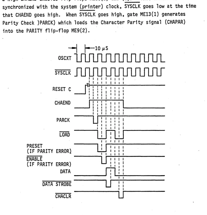
7.4.3 Output Timing
Setting flip-flop CHAEND initiates the transfer of the received character from the shift register to the printer. As shown in Figure 6, a high CHAEND enables flip-flops ME10(1) and (2). Since CHAEND is
synchronized with the system (printer) clock, SYSCLK goes low at the time that CHAEND goes high. When SYSCLK goes high, gate ME13(1) generates Parity Check )PARCK) which loads the Character Parity signal (CHAPAR) into the PARITY flip-flop ME9(2).
---1
1-
10 IlSOSCXT
SYSCLK
RESET
c
~l
I I
CHAEND
PARCK
LOAD
PRESET
(IF PARITY ERROR} ENABLE
(IF PARITY ERROR) DATA
DATA STROBE
CHACLR
u:
I II I
WTW
I IW
I IU
IIn
U
U
When SYSCLK g~es low, flip-flop MElD(l) is toggled set causing LOAD to go low. This enables the parallel inputs to the shift register.
If CHAPAR is high at this time (indicating a parity error), the following action occurs:
1. Signal PRESET goes low placing an octal 100 code
(@
sign atthe parallel input to the shift register.);
.2. PARITY flip-flop ME9(2) is set;
3. When SYSCLK goes high again, gate ME13(2) generates a low ENABLE, which causes a high LOADIN signal out of gate ME12(4);
4. The high LOADIN transfers the @ sign (on the parallel input)
into the shift register.
The next low-going SYSCLK toggles flip-flop MElO(l) reset and MElO(2) set causing LOAD and CNT02 to go high. A high LOAD and CHAEND
gates the shift register outputs to th~ input data lines to the printer.
A high CNT02 enables the EOM/SOM decoders - ME16(l) and (2). If the character in the shift register is an EOM and there is no parity error, then EOMDEC goes low. Similarly for an SOM character, signal SOMDEC goes low.
While SYSCLK is low, if the printer is not busy (BUSY is high and the Busy Enable jumper is used - E27 to E28), a low DATA STROBE is generated at MElI-B. If the printer becomes busy while DATA STROBE is low, the high output from gate MEl5(6) holds ME17-l low. This holds DATA OUT "(ME17-l3) high which allows "the DATA STROBE pulse (5 usee) to
remain high until the next low-going SYSCLK. However, all future DATA STROBE pulses are inhibited until the printer BUSY signal goes high. DATA STROBE is also inhibited if either an EOM or SOM is decoded (EOMOEC or SOMDEC disables gate ME1l(1)).
When SYSCLK goes low again, flip-flops MElO(l) and (2) are both
set enabling gate ME12(2)." This causes the next high-going SYSCLK to reset
C~aracter Clear flip-flop ME14(l). The low CHACLR signal then: 1) clears
flip-flop MEB(2), 2) clears the Character Parity flip-flop ME9(l), and 3)
7.5 STATUS INDICATION
7.5.1 General
When used as a direct input to the printer, the RS232 interface
use~ the Select (SLCT) and BUSY signals from the printer to indicate to the data set the status of the machine. When used as an input to the Centronics
Ring Buffer (option), the RS232 interface used the ~253 and ~229 signals
from the ring buffer for this status indication. In both cases, the reverse channel line is used to prevent transmission of data while the printer (and/or Ring Buffer) is incapable of receiving data. As a
program function, reverse channel is also used to inform the transmitter of a parity error in the received data.
7.5.2 Reverse Channel
Two one-shots are associated with the reverse channel logic: 1) . ME19(2), triggered when reverse channel goes active, holds RCHAN active for
at least 200 milliseconds; 2) ME19(l) prevents an EOM from re-activating reverse channel for at least 200 milliseconds after RCHAN goes inactive.
When the RS232 interface is used as a direct input to the printer, reception of an EOM (low EOMDEC) and no parity error detected in the
received message (low PARITY) sets latch ME24(3) and (4). ·Providing that one-shot ME19(l) has timed out, this condition sets latch ME23(l) and
(2) activating Reverse Channel (low RCHAN).
If the RS232 interface is used as the input to a Ring Buffer,
the accumulation of 253 characters in that buffer ( ~253), indicating that
it is incapable of receiving more data, causes HICNT to go low. This condition also sets latch ME23(l) and (2) activating RCHAN.
When one-shot ME19(2) times out, a Busy signal from the printer (or Ring Buffer) may still hold reverse channel active. If the interface is
used as ~ direct input to the printer, when the EOM which initiated
reverse channel is received, the printer will normally be busy operating on the data received in the preceeding message (signal BUSY will be low).
If the interface is used as input to a Ring Buffer, the BUSY signal
is replaced with signal ( 2!229). A high ~229 signal indicates that the
.Ring Buffer has accumulated more than 229 character.
When the p·ri nter is ready to accept new data (BUSY goes high), or
the number of characters in the Ring Buffer drops below 229 ( ~229 goes
low), and one-shot ME19(2) has timed out, the output of gate ME23(3) goes low. This resets latch ME23(l) and (2) causing RCHAN to go high,deactivating the reverse channel.
The high-going output from ME23(1) fires one-shot ME19(l). The low output from this one-shot inhibits gate ME24(1) for approximately 200 milliseconds. This prevents activating reverse channel for at least 200 msec after reverse channel goes inactive.
7.5.3 Baud Limitation
The 200 millisecond intervals developed by one-shots ME19(1)
and MEI9(2), ensure that a maximum reverse channel rate of 5 baud will
not be exceeded.
8. SCHEMATICS AND ASSEMBLY DRAWING
This section contains the following drawings:
Figure
7 8
9
10 11 12 13 14 15
Schematic Diagram (Sheet 1) Schematic Diagram (Sheet 2) Schematic Diagram (Sheet 3) Schematic Diagram (Sheet 4)
Schematic Diagram (Sheet 5)
Electronics Cavity Assembly
I
t-a \0
I
Refer to tile Ntfllllf", 0' til" IIct'Oil for poufbl. eha"," IIOt
1It 'lICorporattd 01\ tilt. PIli',
~---.---~ RE:SET
C.
ME3(Z)
~ _ _ 7-1J Q ~
5 1473
elk a
_ _ +-,'-10 I( CLR el
~
-f-5V
-M G 12.- 3 ----1...----_
.MEI4-8
PWR PRM
C4
.OSjlf
:to" VI
~---~O~---+---morRIUNo., AND IS NOT TO BE RELEASED OR REPRODUCED WITHOUT WRITTEN PER· MISSION OF CENTRONICS deca - . . - . .
"tOTeS: .4
I. ALL RESISTORS AR.E 114\1'11'0 -"
UNLE55 OTHERWISE. 5Pe.C. .. ·.EO.
2.. saE SH£!.E.TS 4 A .... D 5 FOP.
ADOITIONAL NOTes AND
CHAR-,S
CI~
b
220tof±ov
SEE. NO'TES :3 AMP ... II SCHEMATIC DIAGRAM,
TAL RS232 MULTI- PURPOSE
... !N 2Zf<
SHEET 6 COVER SHEET
Figure 7. Schematic Diagram
"c -...
63004114 -AI N
a
I
. RE.TURN TO tOY
)( P3
[£]
STROBE CHAPA ±ov'1'''' to tile MiIMI,.. 0' tilt.
IKUOft for poulllli ella ... IIOt Itt IlICorporate4 .. tilts PIli.
STROBE
~L()C.K
C DATAO(Q
a
E OA"TA04 15 ME2S
"71199 D"Tp.03 F r.I--7----.-r-l
tu
..J
co
«
z.
MEN IU
~ ...
V lL
9 J: H O,aiTAO I
2-~ V) 21
" 23
CHA END
. LOAD
f..---.LOAD IN
ME s(z)
"7 J
CATAB MEI4(Z) P .. I~ 19 II 15 20 17 16 18 ME7-Z DATA07 OATAO~ OATAOS
THE INFO .... ATION CONTAINED HEREIN .. PROPRIETARY AND I' NOT TO IE RELEAIED OR REPRODUCED WITHOUT W'U"IN PD· MIlliON O'CENTRONICI . . . ...,. . . .
ME ,~(3)
7405
Rl9
~-_--u""'''"--O + 5 V
ME\S(l> 7405
'K
9 ME. 1(. Cit>
OA,A03 t:5e~ _ _ _ _ _ . E oM DEt:
DATA02.---I----'
OATAO' __ ---r-~---~, SOMOEC,
C N T O G - - - + - - -_ _ _ ~
DATA STR06E.
To ME. 11-11
MESO)
J..'----=z:...fD Q CHAEHD
oopc.hlr 7114
" eLI<
741"1
3 CoLI!;
OSC')(T
E.2&
SUSY~I! ' b--:6~"
Z7 £29
CI..R
13
O ' t . ; ( ) - - SYSCLK
CHAC.LR
."USCHEMATI C DIAGRAM, XTAL RS 232 MULTI-PURPOS
-=-
C· ...
6.30041 41ft.
5HEE T 6 COVER 5HEE T 5HEET 2 OF {,
I N .-I EOMOEC PARITY JI"
B B 3 I - - - - . l . " ' - I
C. F S 1----+---'-1
P3
CACAOE
DSTROY
+5 V 221--... - - t - - - - 4 . . - 4 - - - O +~"
·ca
~Pf
+12 V 5
J---_--_-4-_-oCl
+ I c: v CRt•• f.,. to tile
""""'III
Of tilt.steUOII for pollnll. ella .... IIDt
,.t
hlCOt'pOrlted 011 tII'~ PII'.+5'" Mel9
(I)
74'Z3
L - -_ _ _ _ _ _ _ 4~Q. B 2
THE INFORMATION CONTAINED HEREIN IS PROPRIETARY AND'I NOT TO 8E RELEASED OR REPROOUCED WITHOUT WRITTEN PER· MISSION OF CENTRONICS ... CIDIp.
CHAENO
5
JZMEI3~)
e EHABLE
10
CHAPAR. 13
-I- 5 V O-"'*-_~
. DATA OUT
CHAEND
CNT02 ME 10 (Z)
, .. J Q ... I_'-+_-+-t-... 5--4
5 C'.HAC.LR
elK
74'~
L.-~~~~~ Q~13~1-~
C R
~
. L -_ _ _ - - '
PRESET
PWRPRM --+---...
+sv
R,2B 10k
.. C'7
I
50~ftoY
t--... - ME2"-'"
IN~o02
-12 v 4 t---1~--..-__J._-~ -12V
C'2 lo"af
CR2
SHEE T 6 COVER SHEET
JI5
oE-,?)o-~--o---'-I" S A SOMDEC.
EOMDEc:. .
r.---,
C:
1
rl~~~! OSC~T
,12'30 e31 I
I I
L _ .:'~ _"I~
_
JDA,.-A
OUT
cIa
l,oooPF
ME.Z( ... ) +5"1
CHACLR~
ENABLE ~LOAO'N
. P3 MEIS(5)
(~ 253)~ HIC.N,.
"'''SCHEMATIC DIAGRAM
TAL R5232 MULTI-:PUROSE
"c · ..
···63004114"A
SHEET 3 OF 6
I N N
I
~AUO JUMPERS
RATE FROM TO
EI E I E3 EI3
110 ea Ela
,"4 EI4 . E9 EI9
610 E~O
iiI Ell
e.6 Ela
ISO E7 EI7 E4 EI4 EIO £20
EI Ell
E3 EI3
.300 E6 EIB
ecc.
el"-e~ EI9 EIO £20
E~ EI!t
E.~ EI5
GOO e,., e,I,
E& EIS
52 EI2
E'3 EI5
E.' Ell
E9 EI9
E4 EI4
ECO EIG
\050 E1 EI7
ee e.IS
E3 el3
e., E;t 1
(~~~~. i»
EI --.5"""3 E~-Ja..(.lS
EZ-20,u.,S
lEe. 40..,uS
E7--80,u..S
E5-t~0...u5
E(Q-320,lkS
E 4 - G40,uS e9-IZSO,u.s
elo- zS~O.PS
I"'" ...
l"tlOil for polltlll. ella ... t,.t tllCorporate4 OIl tlltl "I'.
~TAL e~ e,,, REMARKS
:Z.MHZ .ODI)lf 470PF SEE HO'TE ~
2MHZ .·OOIAt 170Pf ~EE""OTE3
L2MH2. .oo!.JIf 410PF SEE NOTE?>
'MHz' SEE NOTIi 4
~/" wI"
'MHZ. SFENOTE 4
tJ/A ~II\
"TABl.E.
~)
( S t . ~OT_
TO CONFIGURE JUMPERS
- - ' - - -!.. 2 -10".£'9 :::: D~c:.oDE
SAUD • RA.TE
JUMPER TO GET
APPRO-PRIATE SUM USING TABLe e
iABLE A
BAUO JUMPERS XTAL
RATE FROM TO C~ CI~ REMARKS
E9 EI9 IMH~ SEENOTE~
1!4 1:14 6:"7 En
eB E'6
~/'" ~/,.
IZOO 6:2 e.z
E3 EI!o
e.I au
eg EI9 IMH~ seE" HOTE4.
1760 e'7 EI7
N/'" ·4". ee Ele
E~ C!13
E.g EI9 1M HZ. SEE NOTE 4
IBOO E7 E17. lJ/" ~/"
E2 EIZ.
E4 EI4 IMHZ. SEE NOTE 'I
E(Q Elco 2400 ...e.a ...E.IB
~/" lJ/A
E2 1:12
1:3 EI3
E4 e:.4 1 MHZ. SEENOTE 4
3(,00 e.s £18
\JIlt.. ~/A.
Et Ell
EGo E''- 1 MHZ. SEE HOTt: 4
E5 EI5
<laDO E2 1:12 lJ/A tJ/A. E3 EI3
EG EI" IMHZ SEENOTE4
G800 aB EIB ~/A. tJ J"
EGo E'G IMHZ
~/t\ \J/'" SEE NOTE 4
7200 E.~ EIZ
"TABLE.
1f
J..~It. NO,':' 4 (51ii& \I.IoTe. 4) ,Ae,LE E.
EI--'~S TO CONFIGURE JUMPE.RS e~-e M.-S
e~-4..us
- - ' - -"- 2 -2)-'5 = DECODE
Ee e..u-s
E7 I ;;;--.:.u;s- BAUD·
E5-32..t-tS RATE
~6-{'4 ,...u.s JUMPER TO GET
APPRO-E4-t29 as PRtATE SUM USING
E9 ZSIJ.,us TABLE 0
C'O 512...us
SHEET 6 COVER SHEET
Figure 10. Schematic Diagram
THE INFORMATION CONY AlNED HEREIN II PROPRIETARY AND IS NOT TO 8E RELEASED OR REPRODUCED WITHOUT WRlnEN PER-MISSION O' CENTRONICS .... 0IIIIIjIUtIIr . . . .
BAUD JUMPERS
C,"
RATE FROM 1'0 XTAL C3 REMARKS
E~ EIS IMH~ 5EE t-iOTE4
9000 E7 en
~/It..
6.z. EI2 tJ/'" e:~ EI3
e~ EIS • MHZ. SEE NOTE1
!!J"OO E7 Ell tJ/" lJ/"
E3 EI3
NOTE~ u:'ONT.)
se.e SHEET I FOR. NOTES, A .... O'2,.
3. TABLeS BAND C WILL ee. USED TO CONFIGURE SAUD RATES BELOW 600 BAUD. A "2 MHZ. CRYSTAL WILL. BE STANDARD \NITH C~ AND CI~ .q. BEING TABLES D USED. ~ND E WILL BE USeD TO
CONFIG URE BAUD RAT es GOO SAUD
\ 0 9600 eAUO. A I MH"Z. C;R'Y£)TAL.. ""ILt. BE STANDARD. <:3 AND CIQJ W.ILL NOT BE US~D.
"ltL.
SCHEMATI'C DIAGRAM, XTAL RS 232 MULTt-PURPOSE
-·,c
163004114lA
SHEE T 4 OF 6
I N W I ;
I
I
I I I i I I II
OPTION A e C 0 E F G H :r J I< L M N 0 pFROM TO
E22.· E2.1
EZ2 E'2~
E22 E24
E2Z Ell
E22 £23
EZS E27
EZ8 E29
E32 E~I
E3'2. E30
E?lS E33 E35 E34 E3~ E37
-
--E39 E38 E40 E~5
E41 E35
r
•• ,,, . . . , .. of .. "
I
THE INFORMATION CONTAINED HEREIN ISlecttOll for ponU,I. chi"", lilt PROPRIETARY AND IS NOT TO BE FlElEASEO OR REPRODUCED WITHOUT WRITTEN PER.
,.t tllCO\"1ICW.tH OIl tlltl Pig •• MISSION OF CENTRONICS d8la
-Pl-
~TABLE ] I
JUMPER
SIGNAL IDENTIFICATION
FROM 1 0 FROM TO FROM TO SPARE CHIPS NO.1 oR 2
E2.5 e2~ e.VEN PARITY (NORMAL)
EZ5 EZcc. ODD PARITY (NORMAL)
EZ.5 E2." PAR.ITY DISABLE (DISABLE PRESETTING OF @ SIcc.N)
eZ5 E2Cf EVEN PARITY~ONLY(D'SABLE. PARITy BUT PRINT@ PER CHA~AC 'TER
e25 E24 ODD PARII'f'@ONL'Y(DISA6LI:;: PARIT'( aUT PRINTfu) PER CHARAC.TER)
BUSY ENABLE (NORMAL) eUSY DISABLE (RING BUFFE.R) HICNT ENABLE (RIN~ BUFFER)
HICNT O'SABL.(NORMAL) ENABLES REV.Ct-'. WHEN HICNT 15 NOT useD SELeCT 'N(WHEN SELEC.TED CD IS HELD AT +12")
SELECT OUT(CO IS ALWAYS HELD AT +IZV)(RING BUFFER,) PROTECTiVe GROUND IN
PROTECTIVe GROU .... O FLOATING REVERSE: CHANNEL NORMAL OUTPUT
CO (CONTROLl.EDBY BUSY NORMALL'( -12V.WHEN ACTIVE +12"1) CQ(CONTROLLEC BY BUSY ",",ORMALLV+ 12.V, WH eN Ac.TlVe - 12'1)
' - - SEE NOTE 5
NOTE'S (CO NT .)
SEE S~EETS I AND 4 FOR NOTES , -4
5. ·co",s OATATERM' .... AL READ"{.
t.:.. -e.- POI"-lT USA,COe .,.OT 'S~ICi'e.O
,t.JOlCA"e.~ TH£,,( A~ "-JOT v~o.
T" ....
SCHEMATIC DIAGRAM., XTAL RS232 MULTI-PURPOSE
~.
rc
163004114rA
*--- -.- _ ... --- . _ ... _. ---_ ... - --- ---_.- - _._-_ •..
__
..SHEEr £. COVER SHEEr SHEEr 5 OF 6
I N
~
I
"'''' to CIIt
Nt''''''
01 ~,. leeUOIt 'or ... e ... t~t '!!Corpora," 0It ~h .... .
·£L£CTRONICS CAVITY A55EMB1:.Y
C~OC»IO.-2
WI
r - - - 8
'LEr'
C4- .~" +
...
---_.
__
..-Figure 12.
W3
IlEFE"RENCE DJ;: ... II ... ~$:
SCHF MATIC. OI ... Cii .. " .... -C.300Z~"'7'"
HI-lioNESS ASlOEMIII."'" (WI) OCl30Q~Z5a-2
CABLE ASSE.MBLY :V'l1) 0,"300",'03 POWEFt CABL~ "'~~EI"f.H·( (W3) C.3002zse
El ectroni cs Cavi ty Assembly (101/ lOlA)
I N
U1
I
~I.I
_It ...,.,..,
NoT£ INOT£S:
,. ALL ,NTEc.",.TED CIRCUITS AAI. TY~ICALLY
"-40UNTE.D.
! . MARl< '/8 H'GW alACIC C ... " ... c:T.RS
AND loO.: .... ,. .. APPfllO~ A$ SHOWN.
_....-r._~._(,.
T. -r.. .... An _ _ TT_-a- _ ~ CNLV _ C1' , a" DO MIO " ' " ' tom _
001 8OARO.
SI!£"'OTIt ..
ASH ..IUMPS..~
"G FIfO'" TABLe: a
- , , .. F.X J L . . STANDARD ~VEN PAJl.ITT
- l STI' ... O ... !; ODDP .... n v
-5
-.
114'rt'r ttl til;) IIf9tNltllg of tilt,
IICUOII for po""l. e"' .... IIOt
,.t fllCOI"pOrlttd 0/1 tilts PI •••
.-.-. ....
I - - - t - - - I ;=_-:.
0&
_--..._-_
.
...
_
... __-...---.,..,.
... ...I N 0\ I Item 1 2 3 4 S
-6 7 -8 -9 10 11 12 13 14 15 -16 17 18 -19 20 21 22 23 24 Symbol Cl C2. C4 C3. C18 CS. C6 C7. C16 C10. C12 C9. C11 C13. C20 C21 C8. C14 C15 C17 C19 CR3. CR4 CRI. CR2 J15 MEl. ME2 ME3. ME5 ME9. MEI0 HE4. ME17 ME6 HE7. MEll HE23 ME8. ME14 HEl2. ME24 MEI3. M~16ME15 ME18 HEl9
"'''' q tk ..,IMt", ., &IIts
IICUOII 'or ponlbl. cfla . . . t ret hKorporltH OIl tilts PI •••
Part Number Nomenclature
63004013-1 Component Board 21472003 Capacitor •• 0047 uf 21503003 Capacitor •• 05 uf 21102000 Capacitor. 1000 PF 21471000 Capacitor, 470 PF 21471000 Capacitor, 470 PF 22106002 Capacitor, 10 uf 21104001 Capacitor, .1 uf 21104001 Capacitor •• 1 uf 21104001 Capacitor •• 1 uf 22107002 Capacitor, 100 uf 22107002 Capacitor. 100 uf 22506002 Capacitor. 50 uf 21221000 Capacitor. 220 PF 38100904 Diode. WG 904 38040020 Diode. IN 4002
31230019 Connector. 225-21521-110 35474930 Integrated Circuit 7493 35474730 Integrated Circuit 7473 35474730 Integrated Circuit 7473 35474020 Integrated Circuit 7403 35474300 Integrated Circuit 7430 35474100 Integrated Circuit 7410 35474100 Integrated Circuit 7410 35474740 Integrated Circuit 7474 35474000 Integrated Circuit 7400 35474200 Integrated Circuit 7420 35474050 Integrated Circuit 7405 35474040 "Integrated Circuit 7404 35474123 Integrated Circuit 74123
LIST OF MATERIAL FOR COMPONENT BOARD ASSEMBLY
(Reference: Figure 13)
Quantity Item
1 25
1 26
2 27
2 28
4 29
-
302 31
5"
--
32-
-3
--
331
-1 34
2 35
2
-1 36
2 37
4 38
.
392 40
1 41
3 42
-2 2 2 1 1 1 Symbol ME20. ME21 ME22 ME25 ME26" Ql. Q2 Rl thru RIO R28 Rll, R15 R21, R22 R23. R12. R13 R16. R17 R14. R18 RI9. R20 R25. R27 R24. R26 R29
Yl Yl
'R12
Part Number Nomenclature Quantity 35474080 Integrated Circuit 7408 2 35214891 Integrated Circuit MC1489L 1 35474199 Integrated Circuit 74199 1 35214881 Integrated'Circuit MCH88L 1
38239040 Transistor. 2N3904 2 41103926 Resistor. 10K, J.iW. tlOS 11
41103926 Resistor. 10K, J.iW. tIOS -41682926 Resistor, 6.8K. ~W, tl0S 5 41682926 Resistor, 6.BK, J.iW, fl0S -41682926 Resistor. 6.8K. ~W. tl0l -41222926 Resistor. 2.2K. ~W, tl0S 3
41222926 Resistor. 2.2K. ~W. tl0S -41471926 Resistor. 4700 • l.iW. tlOS 2 41102926 Resistor. IK. l.iW. tIOS 4 41102926 Resistor. lK. l.iW. tl0S -46103910 Resistor, t10S POT 2 41223926 Resistor 22K. ~W. tl0S 1 37816544-1 Crystal •• 2HHz 1 37816544-2 Crystal. IMHz 1
30070000 Solder. 60/40 AR
39610000-5 Wire. Bus No. 22AWG. Solid AR 41152926 Resistor. I.SK. ~. !10% AR
I N
...
I
1e,If' te tMl"""'1II 0 \lit.
I
"CtlOll for Po ..'.l.
t ... lOtI
Itt 'lICorporatod 011 \II .. PI,',
TABLE A
" , [ . , I,..H&
E... e ....
C, .. RI! ... IlK'L QAUD R"'T~
SUI .... OTE 4
9000 JU ... PI:RS
lIT,,1. ca' c,c;, RE .... ARKS
FROM "TO
SOl! ~Il' IMHZ :lEE HOTE1
I!"J Et"f
EZ ~IZ 11QO:yJ wi" wi",
wi" Ii.~ el:!l
IZOO ~~~ ,T."" w/ ..
1-,.' ell . • ~M .. it .001."1 170",. SEE NOTE ~
~OO ~~.
*
'1SAee " ... 4 rosMe:~
~:;-~OO r-{~ -lfi:: I . . . . ~
EiiJ "'S
~EE t-<OTE ...
t-i~ ::!- ,-.. fIl wi'" wi'"
,,~. E'it
I.~ " , .
~J"!'!-SEE t-<OTEo 4
~ ... ~~ tlt.~i)
~5;iiS 1 'TO CONFIGU".I:. JU"" ... 'to
~!fcf:Js
1-1-
-:-z -I~t ,~o~~')[,£~~~ BAUD
~TE
~'.'.s
J";";~~;' T;G';;" ~""'R':>-~
EQ-~ .. ,."u:
ri::4 , ~ I': PA'~'T;: !5L;M \.,;5 • ...,.. !
I i i ' ~IZ.RO.!'!' , Ae~1:. eo j
1::..0 --~~Go:;.ll;
f -..
17~O
I !I 00
t400
3"="
.. ~oo
"eoo
7200
OPTION FROM ..tUMPER·l!iil-. ~.
'0 FH.OM TO F~OM TO Fk~',: "f0
A
_22
E~' le~:; EeGo8 E:U: IEe- e ... I.e.
C EZZ 5.21 ~Z5 Ilt4
~ .EZ2
~~~ ~g- Hl---I! IitZ
F E.ZS ~",7
• a!~ Cit,
.
:x. EIZ E.ao
-.
'" 5:.55 "31
I.. 1~3Qo
IES-M
N E3' ... 8
P £11 £35
liZ 1.11
e~. EI.!! I ... H1
w/lt. 0.'''' SEENOT"-'"
9600 e"z ~J ,Te.-M
.. :0 to,)
eo' el'
1.3 Eill SEE NOTI! 4
.. I",
., ~ 'MHZ -1:.7- EI1
, ... "
E ... Il, .. w/ ..
E3 E., 3
w/" 51.E MOlE"" "-, t..' ,t-At-t7..
;:'7 EI , ... " Nt .. £2 E'Z
j ; 4 1.14 SEt: Nu ,to 4
W/"
lOCO E~.
w/ ... e.e E·a ~"fIl
~~- .~~
r£.-_~!.L
.... £14 I .... HL :!lEe NOTE ..
Ill" lEU'
~I ~I!..-... '1 N/" 04/"
~ -%:. 'MH7 ~Er, •• 01 . . .
t*-{}}-,,.... a ... / .. w,,,,
~ ..
.. Go "-IGo .Jr0,4 . . .
"'/A "eE N-:lT1.1
I"f" r1WU ~9 "/~
'M~:z. .;c.l. ~.J , 4
,~ ;=]it rI8.O!J9 ... /,. "'1'"
~~~~l
I 1..1<5
~ 1 ... "
2- 4..uS
:e_ e.u
·IGo..u
,!I 3&MS EC.
..
~.I~"
12 .. -"
~, .2'. 5 11:.1:' ·,.z
TABLE ] I
!;PARE CHIf> "0. l O R .
~~:~4)
TO CONI=I&UI<~. JI..' .... pE. .... ~
BA~D + 2 -~~co.:::t:~ "'''Te:
JUt-APE'" TO GE.T
APPRO-PRI""TS. SU ... USING
T .... SLIi D
SI6NAL IDEI'iTIJ=ICATION
EVil ... P"RIT'( ,. NORMI"I..
....
PAIlt.ITY D' .... BL.. IS"'BLIi: P~IE:S~TTINQ 0"- evSIGN
v N ,.. IT"'" ON ';'<t I' L P""," ,,..., T INT I? CHAR.A
000 P"RITY tWo ONLY Ol5"&I.E PIIAIT'( eUT PRI"'T~ peN C .... I''' ... ::T!!: .... ) U .. L ... 0 to! I.
eu • I. ,,., .... ~ ~U .. F1: ...
H.e", _e.N" ~\.E (R'N~ B ,,,,,"!!" ...
.... ICNT O' NO M I. IENAB .~s v. c... ... ... ""eNT I~ .... OT ~ED
.... ' N La I .... •
:5I!Le"T OUT ~D IS "t.W"'f5 .... .:LO ... T "'.'1 RING SUFFER'
T '" _ .... oU"" IN T .""'0 ... Ne "" 0" ING
R IE".'" 5 £ C"'''NNEL NO .. I.. TP T
ON at... U,,«No ALL: - VW'" C"I +t
C C.O .... "TROI. .EO BY BUSY NO"''''AI.I..''f "IZ"."''''~''' "CT,,,-. -1&'1
l . . VIIIONi
NOTI!:~ (c.0"'"T.)
!lEE SHE~T I FOR ,,",OT£5 1,_ ' "
3. T"'IIL1t!l II AHD C WILL .,~ USI!D TO cO ... PIGURE
.,AUD RATE BELOW " 0 0 "AUD. " .aMHZ.. JlT"L \/'I'LL BE ST""'OARD WITH C!I ""'D <:140
eI!It'4Q USED.
4. "TI'BL£:5 D " ... D C WILL BE USED TO CONFIGURE
BAUD RATes . 0 0 B"'UD To St600BAUD. " I .... H:. MoT ... \" WILL BE STANDARD. C!I AND C,. WILL NOT I!Ut useD.
.5. ·C 0 · ' 5 OAT ~ 'TERMINAL RE~O"".
~ . . . . Pot..". ~. Io.I!:I'T -.o~1IQ I~ ~ . . . wszr
u.~.
1
_--.... ... - - ·
...,. .... ,. ....
,..-..--
... - " -...
_
..
---1£ 163004113 fA
0 0 4 ~e, IJN 'f(":;
-I N
ex>
I
Jef.,. .. die " " _ ' " .f .. f.
IeCU .. for .. "',,.
eM,.._
,.t tllCllt"JlOl".tM .. "'fa ...
---.. ---_ ... --.. --.. ---·--r---.~.~V~IS~IO~N~S---..
~ "v :10' j;-.so - - - 1
NOTES:
I. ~"RIP ALL EHOS .250 J'HD TIN BEFORE "'SSEMSL't.
2. CUT JACKET INSULATION BACK •• soo
4i-1S
i
INCHES eEFORE A5SEM6LINlii W.TH CONNeCTOR,
ITEM 2 .
3. CUT OFF BLACK .... ND WHITE W'RES TO JACKET
INSULATION ON 60TH EHCS eEFORE ASSEMBLY.
WIRING OIAIDRAM
~
.0'
"'O."l
15 ~I~
BROWN P AA B& CA CC "8 CF 5"
+ II\/O~TS
CO
,..
7 I- FI£D
~ o"" ... e ~ ~ yellOW
~
7 \iRUiN
I- eLue
~ ~ ~ ".OL.ET
~,
H1i
fT.i
~
~~.
)
7~TE' -- - TO 5P£"ICEA
r=-~ 0
~ GiOIII."'"
,1:-~ 4 ~ ~ ~
~ p
R S -.-!-. r!-~ • ~ ~ 7 --..!. ..!. ~ ~ r!-!; ~ ~ .5 ~ E
~ " ~
~
2314 i!5 Item 1 2 3 4 S· 6 7 8 9
Figure 15. cab~~)AssemblY
(W4)
~
Symbol
P16
PIS
~ ~~~~~~~~~~~~ ____ -L __ _ L _ _
Part Number Nomenclature Quantity
39660009 Cable. 1/0 Conductor 10 ft. 3IJ00432 Connector. 25 Pin 1
31240432 Dataphone Hood 1
62000000-1 Connector. Finger Board 1 63004100-1 Plate, Connector 1
36150000 Strain Relief'Bushing 1 39640000-4 Wire. Hook-Up. 22 AWS. WHT 6 fn. 39640000-4 Wire, Hook-Up. 22 AWG. BLK 6 in.
30700000 Solder AR
1 .... - . - - - · _ n A l l V _ _ OII _ _ _ 0 1 - - ' _ _ _ JKlTYD . . ~ _ _
ED"~ ~''''"T '=>'"" ~waOO'lo'O"lo-\ oV' """""T"'~'~
1 1-1-1 ... 1
...
I·· .. •• ..... _ _ ...
....
..
u.
...
C~
.,ICtfII .... ~==
....
ft..
----
...
-.. , ... CABLE ASSEMBLY
....
~- .nt.11.• nt.06 - - t RS 232 INTERFACE:(w4
~\\'~"''I. ' D \ \
--
1-= \''016"3004103 IA ;vx,\\O"'- "!!.oaD• ..,&111.
_
...
""oa r-... II.\ ... ~',. It. -'}j~o
oo
...o
Fingerboard Connector (PIS)Pin 1
Pin 3
Pin 4
Pin 6
Pin 7
Pin 8
Pin 11
Pin A
Pin B
Pin E
Data Set Connector
. (P16)
Pin 1
Pin 3
Pin 4
Pin 6
Pin 7
Pin 8
Pin 11
Pin 20
'9. INTERFACE CONNECTOR
Signal Name ·AA BB CA CC AS CF SA CD Source Printer Data Set
Printer
Data Set
Printer Data Set
Printer
Printer Printer Printer
Signal Description
Protective Ground
Received Data: A -V* is. a Mark and a +V is a Space. When released, this line should be in the Mark condition.
Request to Send: This line is held at -V. .
Data Set Ready: A +V on
this line allows the printer interface to accept data from the dataset.
Signal Ground
Data Carrier Detector: A
+V on this line allows the printer interface to accept data from the data set. Reverse Channel: Used for transmitting printer status to the data set. It is
nonmally in a Mark
(-V)
condition. After a line of data is received, this line
~oes to a Space condition (+V) until the printer is able to receive data again. To Speaker
To Speaker
Data Terminal Ready: A +V on this line indicates that the printer is selected.
All other connector pins are open.
Mnemonic AA AB BB BUSY CA CC CD CF CHACLR CHAEND CNT02 DACADE DATAOI-08 DATAl-8 DATA OUT DATA STROBE DSTRDY
ENABLE
EOMDEC
HIM
LOAD LOAD IN
Source* J15-1 JI5-7 J15-3 P4-3 ME26-8 Jl5-6 ME26(3) J1S-8 ME14-5
ME8-5 '
ME10-12
ME22-3
ME25
10. GLOSSARY
Protective ground Signal ground
Description
Received Data line from data set.
Status line from the printer indicating that the printer is busy performing an operation.
Request to Send status line to the data set. Held low when printer is operational.
Data Set Ready status line from the data set. A high allows the interface to accept data. Data Terminal Ready status line to the data
set. A high indicates that the interface is
prepared to accept data.
Data Carrier Detect from data set.
A
highallows the interface to receive data. Character Clear - Indicates the end of a parallel loading sequence to the printer.
Character - A 40 usec pulse indicating the
end of a character.
Timing signal used during the parallel loading operation and EOM or SOM decoding.
Data Carrier Detect - A DC level indicating the
data carrier signal is present at the data set. Eight output data lines from the shift register.
ME20t ME21 Eight gated data lines to the output connector.
ME17-13 . Signal used to inhibit or enable data strobe.
MEll-8 Pulse used to clock data into the printer (5 us)
ME22-6 Data Set Ready - DC level indicating the data
set is in a ready condition.
ME13-8 Pulse used to generate a clock for the loading
of an @ into the shift register in case of a
character parity error.
ME16-8 EOM Decode - Decoded signal indicating the end
of a transmitted message.
MEl8-10 High Count - Buffered signal 253 from Ring Buffer.
MEIO-8 MEl2-ll
Enables the parallel inputs to the shift register.
Clocks parallel data into shift registe~.
*ME26-8 signifies element ME26 pin 8
o
10. GLOSSARY (Con It)Mnemonic Source Description
ODDCNT ME5-8 Odd Count - Used to block every other decoded
pulse and to clock the End of Character flip-flop.
OSCCLK ME22-ll A .2MHz or lMHz crystal controlled clock used
a to generate to strobe; Clocks the serial data
into the shift register.
OSCXT P4-H External Oscillator - 100 KHz oscillator
output from printer.
PARCK ME12-8 Parity Check - A pulse used to load character
parity (CHAPAR) into the PARITY flip-flop.
PARITY ME9-9 A DC level used to indicate a parity error
during the received message.
-PRESET MEll-12 A pulse used to force an octal 100
(@
sign) atthe parallel inputs to the shift register, if a parity error was detected in the last character.
PWRPRM C17 Power Prime - Level used to prime the interface
electronics when power is first applied.
RCHAN ME24-6 Reverse Channel - A 200 usec (minimum) pulse
used to indicate to the transmitting device, the status of the interface and of the received data.
RECDAT ME22-8 Received Data line (buffered).
RES ETC ME7-S Reset Counter - Used to reset the baud coun"ter
that generates the strobe.
SA ME2S-S Reverse Channel line to data set.
SLCT P4-F Select status line from the printer.
SOMDEC MElS-S SOM Decode - A decoded signal jndicating the
beginning of a transmitted message.
STROBE ME4-l0 A IllS or 5~S pulse used to load the incoming
serial data into the shift register.
STROBE ME4-l3 A IpS or 5 usec pulse used to clear the CHAEND
flip-flop.
SYSCLK ME18-l2 System Clock - A 100 KHz clock derived from OSCXT,
used to control the data loading sequence to the printer.
229 P4-3 :::229 Characters - Status line from the ring
buffer indicating that the buffer is approaching maximum capacity.
o
253 P3-2l :::253 Characters - Status line from the ringD
/ "