WP-01197-2.0 White Paper
© 2013 Altera Corporation. All rights reserved. ALTERA, ARRIA, CYCLONE, HARDCOPY, MAX, MEGACORE, NIOS, QUARTUS and STRATIX words and logos are trademarks of Altera Corporation and registered in the U.S. Patent and Trademark Office and in other countries. All other words and logos identified as trademarks or service marks are the property of their respective holders as described at www.altera.com/common/legal.html. Altera warrants performance of its semiconductor products to current specifications in accordance with Altera's standard warranty, but reserves the right to make changes to any products and services at any time without notice. Altera assumes no responsibility or liability arising out of the application or use 101 Innovation Drive
ISO 9001:2008 Registered
Radar Processing: FPGAs or GPUs?
While general-purpose graphics processing units (GP-GPUs) offer high rates of peak floating-point operations per second (FLOPs), FPGAs now offer competing levels of floating-point processing. Moreover, Altera® FPGAs now support OpenCL™, a leading programming language used with GPUs.
Introduction
FPGAs and CPUs have long been an integral part of radar signal processing. FPGAs are traditionally used for front-end processing, while CPUs for the back-end
processing. As radar systems increase in capability and complexity, the processing requirements have increased dramatically. While FPGAs have kept pace in increasing processing capabilities and throughput, CPUs have struggled to provide the signal processing performance required in next-generation radar. This struggle has led to increasing use of CPU accelerators, such as graphic processing units (GPUs), to support the heavy processing loads.
This white paper compares FPGAs and GPUs floating-point performance and design flows. In the last few years, GPUs have moved beyond graphics become powerful floating-point processing platforms, known as GP-GPUs, that offer high rates of peak FLOPs. FPGAs, traditionally used for fixed-point digital signal processing (DSP), now offer competing levels of floating-point processing, making them candidates for back-end radar processing acceleration.
On the FPGA front, a number of verifiable floating-point benchmarks have been published at both 40 nm and 28 nm. Altera’s next-generation high-performance FPGAs will support a minimum of 5 TFLOPs performance by leveraging Intel’s 14 nm Tri-Gate process. Up to 100 GFLOPs/W can be expected using this advanced
semiconductor process. Moreover, Altera FPGAs now support OpenCL, a leading programming language used with GPUs.
Peak GFLOPs Ratings
Current FPGAs have capabilities of 1+ peak TFLOPs(1), while AMD and Nvidia’s latest GPUs are rated even higher, up to nearly 4 TFLOPs. However, the peak GFLOPs or TFLOPs provides little information on the performance of a given device in a particular application. It merely indicates the total number of theoretical floating-point additions or multiplies which can be performed per second. This analysis indicates that FPGAs can, in many cases, exceed the throughput of GPUs in algorithms and data sizes common in radar applications.
Page 2 Algorithm Benchmarking
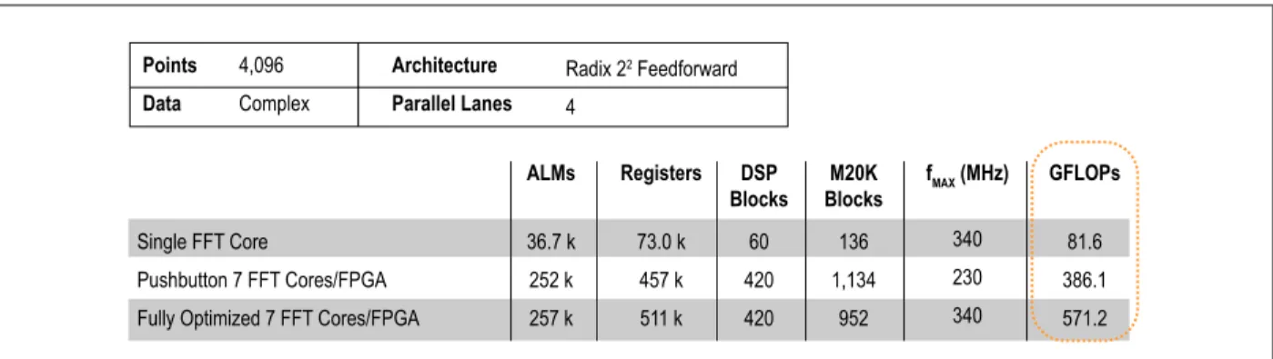
A common algorithm of moderate complexity is the fast Fourier transform (FFT). Because most radar systems perform much of their processing in the frequency domain, the FFT algorithm is used very heavily. For example, a 4,096-point FFT has been implemented using single-precision floating-point processing. It is able to input and output four complex samples per clock cycle. Each single FFT core can run at over 80 GFLOPs, and a large 28 nm FPGA has resources to implement seven such cores. However, as Figure 1 indicates, the FFT algorithm on this FPGA is nearly
400 GFLOPs. This result is based on a “push button” OpenCL compilation, with no FPGA expertise required. Using logic-lock and Design Space Explorer (DSE)
optimizations, the seven-core design can approach the fMAX of the single-core design, boosting it to over 500 GFLOPs, with over 10 GFLOPs/W using 28 nm FPGAs.
This GFLOPs/W result is much higher than achievable CPU or GPU power efficiency. In terms of GPU comparisons, the GPU is not efficient at these FFT lengths, so no benchmarks are presented. The GPU becomes efficient with FFT lengths of several hundred thousand points, when it can provide useful acceleration to a CPU. However, the shorter FFT lengths are prevalent in radar processing, where FFT lengths of 512 to 8,192 are the norm.
In summary, the useful GFLOPs are often a fraction of the peak or theoretical GFLOPs. For this reason, a better approach is to compare performance with an algorithm that can reasonably represent the characteristics of typical applications. As the complexity of the benchmarked algorithm increases, it becomes more
representative of actual radar system performance.
Algorithm Benchmarking
Rather than rely upon a vendor’s peak GFLOPs ratings to drive processing technology decisions, an alternative is to rely upon third-party evaluations using examples of sufficient complexity. A common algorithm for in space-time adaptive processing (STAP) radar is the Cholesky decomposition. This algorithm is often used in linear algebra for efficient solving of multiple equations, and can be used on correlation matrices.
Figure 1. Stratix V 5SGSD8 FPGA Floating-Point FFT Performance
Points Data 4,096 Complex Architecture Parallel Lanes Radix 22 Feedforward 4 Single FFT Core Pushbutton 7 FFT Cores/FPGA Fully Optimized 7 FFT Cores/FPGA
36.7 k 252 k 257 k 73.0 k 457 k 511 k 60 420 420 136 1,134 952 81.6 386.1 571.2 ALMs Registers DSP Blocks M20K Blocks fMAX (MHz) GFLOPs 340 230 340
Algorithm Benchmarking Page 3
The Cholesky algorithm has a high numerical complexity, and almost always requires floating-point numerical representation for reasonable results. The computations required are proportional to N3, where N is the matrix dimension, so the processing requirements are often demanding. As radar systems normally operate in real time, a high throughput is a requirement. The result will depend both on the matrix size and the required matrix processing throughput, but can often be over 100 GFLOPs.
Table 1 shows benchmarking results based on an Nvidia GPU rated at 1.35 TFLOPs, using various libraries, as well as a Xilinx Virtex6 XC6VSX475T, an FPGA optimized for DSP processing with a density of 475K LCs. These devices are similar in density to the Altera FPGA used for Cholesky benchmarks. The LAPACK and MAGMA are commercially supplied libraries, while the GPU GFLOPs refers to the OpenCL implementation developed at University of Tennessee(2). The latter are clearly more optimized at smaller matrix sizes.
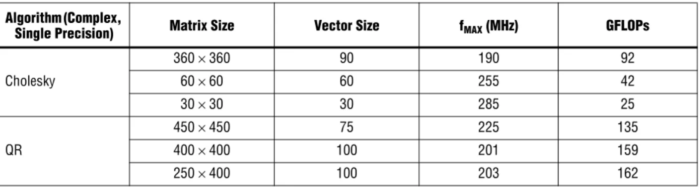
A mid-size Altera Stratix® V FPGA (460K logic elements (LEs)) was benchmarked by Altera using the Cholesky algorithm in single-precision floating-point processing. As shown in Table 2, the Stratix V FPGA performance on the Cholesky algorithm is much higher than Xilinx results. The Altera benchmarks also include the QR decomposition, another matrix processing algorithm of reasonable complexity. Both Cholesky and QRD are available as parameterizable cores from Altera.
Table 1. GPU and Xilinx FPGA Cholesky Benchmarks(2)
Matrix LAPACK GFLOPs MAGMA GFLOPs GPU GFLOPs FPGA GFLOPs
512 (SP) 512 (DP) 19.49 11.99 22.21 20.52 58.40 57.49 19.23 768 (SP) 768 (DP) 29.53 18.12 38.53 36.97 81.87 54.02 20.38 1,024 (SP) 1,024 (DP) 36.07 22.06 57.01 49.60 67.96 42.42 21.0 2,048 (SP) 2,048 (DP) 65.55 32.21 117.49 87.78 96.15 52.74 —
Table 2. Altera FPGA Cholesky and QR Benchmarks Algorithm (Complex,
Single Precision) Matrix Size Vector Size fMAX (MHz) GFLOPs
Cholesky 360 × 360 90 190 92 60 × 60 60 255 42 30 × 30 30 285 25 QR 450 × 450 75 225 135 400 × 400 100 201 159 250 × 400 100 203 162
Page 4 GPU and FPGA Design Methodology
It should be noted that the matrix sizes of the benchmarks are not the same. The University of Tennessee results start at matrix sizes of [512×512], while the Altera benchmarks go up to [360x360] for Cholesky and [450x450] for QRD. The reason is that GPUs are very inefficient at smaller matrix sizes, so there is little incentive to use them to accelerate a CPU in these cases. In contrast, FPGAs can operate efficiently with much smaller matrices. This efficiency is critical, as radar systems need fairly high throughput, in the thousands of matrices per second. So smaller sizes are used, even when it requires tiling a larger matrix into smaller ones for processing.
In addition, the Altera benchmarks are per Cholesky core. Each parameterizable Cholesky core allows selection of matrix size, vector size, and channel count. The vector size roughly determines the FPGA resources. The larger [360×360] matrix size uses a larger vector size, allowing for a single core in this FPGA, at 91 GFLOPs. The smaller [60×60] matrix uses fewer resources, so two cores could be implemented, for a total of 2×42 = 84 GFLOPs. The smallest [30×30] matrix size permits three cores, for a total of 3×25 = 75 GFLOPs.
FPGAs seem to be much better suited for problems with smaller data sizes, which is the case in many radar systems. The reduced efficiency of GPUs is due to
computational loads increasing as N3, data I/O increasing as N2, and eventually the I/O bottlenecks of the GPU become less of a problem as the dataset increases. In addition, as matrix sizes increase, the matrix throughput per second drops dramatically due to the increased processing per matrix. At some point, the throughput becomes too low to be unusable for real-time requirements of radar systems.
For FFTs, the computation load increases to N log2 N, whereas the data I/O increases as N. Again, at very large data sizes, the GPU becomes an efficient computational engine. By contrast, the FPGA is an efficient computation engine at all data sizes, and better suited in most radar applications where FFT sizes are modest, but throughput is at a premium.
GPU and FPGA Design Methodology
GPUs are programmed using either Nvidia’s proprietary CUDA language, or an open standard OpenCL language. These languages are very similar in capability, with the biggest difference being that CUDA can only be used on Nvidia GPUs.
FPGAs are typically programmed using HDL languages Verilog or VHDL. Neither of these languages is well suited to supporting floating-point designs, although the latest versions do incorporate definition, though not necessarily synthesis, of floating-point numbers. For example, in System Verilog, a short real variable is analogue to an IEEE single (float), and real to an IEEE double.
DSP Builder Advanced Blockset
Synthesis of floating-point datapaths into an FPGA using traditional methods is very inefficient, as shown by the low performance of Xilinx FPGAs on the Cholesky algorithm, implemented using Xilinx Floating-Point Core Gen functions. However, Altera offers two alternatives. The first is to use DSP Builder Advanced Blockset, a Mathworks-based design entry. This tool contains support for both fixed- and floating-point numbers, and supports seven different precisions of floating-point processing, including IEEE half-, single- and double-precision implementations. It
GPU and FPGA Design Methodology Page 5
also supports vectorization, which is needed for efficient implementation of linear algebra. Most important is its ability to map floating-point circuits efficiently onto today’s fixed-point FPGA architectures, as demonstrated by the benchmarks
supporting close to 100 GFLOPs on the Cholesky algorithm in a midsize 28 nm FPGA. By comparison, the Cholesky implementation on a similarly sized Xilinx FPGA without this synthesis capability shows only 20 GFLOPs of performance on the same algorithm(2).
OpenCL for FPGAs
OpenCL is familiar to GPU programmers. An OpenCL Compiler(3) for FPGAs means that OpenCL code written for AMD or Nvidia GPUs can be compiled onto an FPGA. In addition, an OpenCL Compiler from Altera enables GPU programs to use FPGAs, without the necessity of developing the typical FPGA design skill set.
Using OpenCL with FPGAs offers several key advantages over GPUs. First, GPUs tend to be I/O limited. All input and output data must be passed by the host CPU through the PCI Express® (PCIe®) interface. The resulting delays can stall the GPU processing engines, resulting in lower performance.
OpenCL Extensions for FPGAs
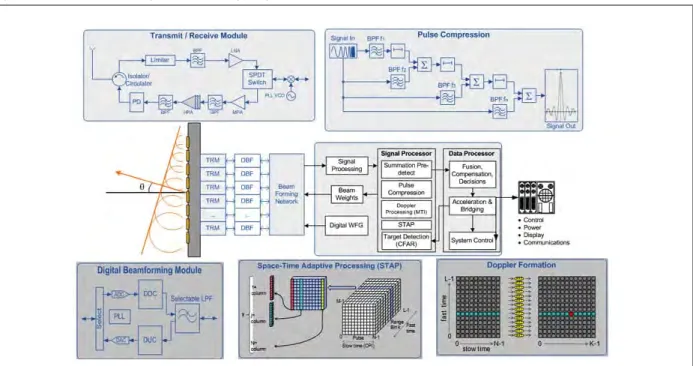
FPGAs are well known for their wide variety of high-bandwidth I/O capabilities. These capabilities allow data to stream in and out of the FPGA over Gigabit Ethernet (GbE), Serial RapidIO® (SRIO), or directly from analog-to-digital converters (ADCs) and digital-to-analog converters (DACs). Altera has defined a vendor-specific extension of the OpenCL standard to support streaming operations. This extension is a critical feature in radar systems, as it allows the data to move directly from the fixed-point front-end beamforming and digital downconversion processing to the floating-point processing stages for pulse compression, Doppler, STAP, moving target indicator (MTI), and other functions shown in Figure 2. In this way, the data flow avoids the CPU bottleneck before being passed to a GPU accelerator, so the overall processing latency is reduced.
Page 6 GPU and FPGA Design Methodology
FPGAs can also offer a much lower processing latency than a GPU, even independent of I/O bottlenecks. It is well known that GPUs must operate on many thousands of threads to perform efficiently, due to the extremely long latencies to and from memory and even between the many processing cores of the GPU. In effect, the GPU must operate many, many tasks to keep the processing cores from stalling as they await data, which results in very long latency for any given task.
The FPGA uses a “coarse-grained parallelism” architecture instead. It creates multiple optimized and parallel datapaths, each of which outputs one result per clock cycle. The number of instances of the datapath depends upon the FPGA resources, but is typically much less than the number of GPU cores. However, each datapath instance has a much higher throughput than a GPU core. The primary benefit of this approach is low latency, a critical performance advantage in many applications.
Another advantage of FPGAs is their much lower power consumption, resulting in dramatically lower GFLOPs/W. FPGA power measurements using development boards show 5-6 GFLOPs/W for algorithms such as Cholesky and QRD, and about 10 GFLOPs/W for simpler algorithms such as FFTs. GPU energy efficiency
measurements are much hard to find, but using the GPU performance of 50 GFLOPs for Cholesky and a typical power consumption of 200 W, results in 0.25 GFLOPs/W, which is twenty times more power consumed per useful FLOPs.
For airborne or vehicle-mounted radar, size, weight, and power (SWaP)
considerations are paramount. One can easily imagine radar-bearing drones with tens of TFLOPs in future systems. The amount of processing power available is correlated with the permissible resolution and coverage of a modern radar system.
GPU and FPGA Design Methodology Page 7
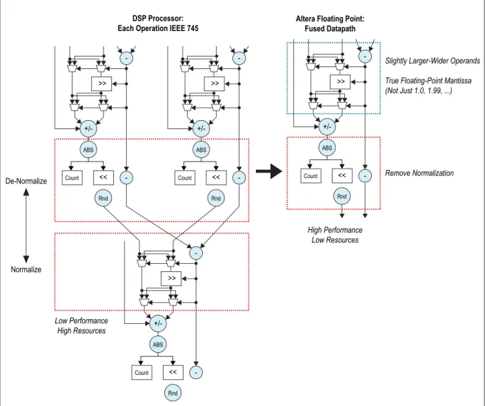
Fused Datapath
Both OpenCL and DSP Builder rely on a technique known as “fused datapath” (Figure 3), where floating-point processing is implemented in such a fashion as to dramatically reduce the number of barrel-shifting circuits required, which in turn allows for large scale and high-performance floating-point designs to be built using FPGAs.
To reduce the frequency of implementing barrel shifting, the synthesis process looks for opportunities where using larger mantissa widths can offset the need for frequent normalization and denormalization. The availability of 27×27 and 36×36 hard multipliers allows for significantly larger multipliers than the 23 bits required by single-precision implementations, and also the construction of 54×54 and 72×72 multipliers allows for larger than the 52 bits required for double-precision
implementations. The FPGA logic is already optimized for implementation of large, fixed-point adder circuits, with inclusion of built-in carry look-ahead circuits.
Figure 3. Fused Datapath Implementation of Floating-Point Processing
Low Performance High Resources
DSP Processor: Each Operation IEEE 745
>> - +/-ABS -<< Count Rnd >> - +/-ABS -<< Count Rnd >> - +/-ABS -<< Count Rnd De-Normalize Normalize >> - +/-ABS -<< Count Rnd
Altera Floating Point: Fused Datapath
Slightly Larger-Wider Operands True Floating-Point Mantissa (Not Just 1.0, 1.99, ...)
Remove Normalization
High Performance Low Resources
Page 8 GPU and FPGA Design Methodology
Where normalization and de-normalization is required, an alternative implementation that avoids low performance and excessive routing is to use
multipliers. For a 24 bit single-precision mantissa (including the sign bit), the 24×24 multiplier shifts the input by multiplying by 2n. Again, the availability of hardened multipliers in 27×27 and 36×36 allows for extended mantissa sizes in single-precision implementations, and can be used to construct the multiplier sizes for double-precision implementations.
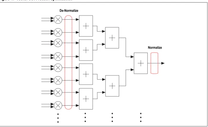
A vector dot product is the underlying operation consuming the bulk of the FLOPs used in many linear algebra algorithms. A single-precision implementation of length 64 long vector dot product would require 64 floating-point multipliers, followed by an adder tree made up of 63 floating-point adders. Such an implementation would require many barrel shifting circuits.
Instead, the outputs of the 64 multipliers can be denormalized to a common exponent, being the largest of the 64 exponents. Then these 64 outputs could be summed using a fixed-point adder circuit, and a final normalization performed at the end of the adder tree. This localized-block floating-point processing dispenses with all the interim normalization and denormalization required at each individual adder, and is shown in Figure 4. Even with IEEE 754 floating-point processing, the number with the largest exponent determines the exponent at the end, so this change just moves the exponent adjustment to an earlier point in the calculation.
Figure 4. Vector Dot Product Optimization De-Normalize
GPU and FPGA Design Methodology Page 9
However, when performing signal processing, the best results are found by carrying as much precision as possible for performing a truncation of results at the end of the calculation. The approach here compensates for this sub-optimal early
denormalization by carrying extra mantissa bit widths over and above that required by single-precision floating-point processing, usually from 27 to 36 bits. The mantissa extension is performed with floating-point multipliers to eliminate the need to normalize the product at each step.
1 This approach can also produce one result per clock cycle. GPU architectures can produce all the floating point multipliers in parallel, but cannot efficiently perform the additions in parallel. This inability is due to requirements that say different cores must pass data through local memories to communicate to each other, thereby lacking the flexibility of connectivity of an FPGA architecture.
The fused datapath approach generates results that are more accurate that conventional IEEE 754 floating-point results, as shown by Table 3.
These results were obtained by implementing large matrix inversions using the Cholesky decomposition algorithm. The same algorithm was implemented in three different ways:
■ In MATLAB/Simulink with IEEE 754 single-precision floating-point processing. ■ In RTL single-precision floating-point processing using the fused datapath
approach.
■ In MATLAB with double-precision floating-point processing.
Double-precision implementation is about one billion times (109) more precise than single-precision implementation.
This comparison of MATLAB single-precision errors, RTL single-precision errors, and MATLAB double-precision errors confirms the integrity of the fused datapath approach. This approach is shown for both the normalized error across all the complex elements in the output matrix and the matrix element with the maximum error. The overall error or norm is calculated by using the Frobenius norm:
1 Because the norm includes errors in all elements, it is often much larger than the
Table 3. Cholesky Decomposition Accuracy (Single Precision)
Complex Input Matrix Size (n x n) Vector Size Err with MATLAB Using
Desktop Computer
Err with DSP Builder Advanced Blockset-Generated RTL 360 x 360 50 2.1112e-006 1.1996e-006 60 x 60 100 2.8577e-007 1.3644e-007 30 x 30 100 1.5488e-006 9.0267e-008 E F eij2 j=1 n
i=1 n
=Page 10 Conclusion
In addition, the both DSP Builder Advanced Blockset and OpenCL tool flows transparently support and optimize current designs for next-generation FPGA architectures. Up to 100 peak GFLOPs/W can be expected, due to both architecture innovations and process technology innovations.
Conclusion
High-performance radar systems now have new processing platform options. In addition to much improved SWaP, FPGAs can provide lower latency and higher GFLOPs than processor-based solutions. These advantages will be even more dramatic with the introduction of next-generation, high-performance computing-optimized FPGAs.
Altera’s OpenCL Compiler provides a near seamless path for GPU programmers to evaluate the merits of this new processing architecture. Altera OpenCL is 1.2 compliant, with a full set of math library support. It abstracts away the traditional FPGA challenges of timing closure, DDR memory management, and PCIe host processor interfacing.
For non-GPU developers, Altera offers DSP Builder Advanced Blockset tool flow, which allows developers to build high-fMAX fixed- or floating-point DSP designs, while retaining the advantages of a Mathworks-based simulation and development environment. This product has been used for years by radar developers using FPGAs to enable a more productive workflow and simulation, which offers the same fMAX performance as a hand-coded HDL.
Further Information
1. White Paper: Achieving One TeraFLOPS with 28-nm FPGAs:
www.altera.com/literature/wp/wp-01142-teraflops.pdf
2. Performance Comparison of Cholesky Decomposition on GPUs and FPGAs, Depeng Yang, Junqing Sun, JunKu Lee, Getao Liang, David D. Jenkins, Gregory D. Peterson, and Husheng Li, Department of Electrical Engineering and Computer Science, University of Tennessee:
saahpc.ncsa.illinois.edu/10/papers/paper_45.pdf
3. White Paper: Implementing FPGA Design with the OpenCL Standard:
www.altera.com/literature/wp/wp-01173-opencl.pdf
Acknowledgements
Document Revision History Page 11
Document Revision History
Table 4 shows the revision history for this document.
Table 4. Document Revision History
Date Version Changes
May 2013 2.0 Minor text edits. Updated Table 2 and Table 3. April 2013 1.0 Initial release.