Sequencing Power Supplies in
Multiple Voltage Rail Environments
David Daniels
Dirk Gehrke
Mike Segal
ABSTRACTDesigners must consider timing and voltage differences during power up and power down in systems where multiple power rails are involved. A simple example would be a single DSP with its core and I/O voltages, requiring power supply sequencing. The possibility for a latch-up failure or excessive current draw exists when power supply sequencing is not designed properly. The trigger for latch-up may occur if power supplies are applied at different potentials of the core and I/O interfaces. This paper addresses some of the more common sequencing requirements of digital signal processing (DSPs), field programmable gate arrays (FPGAs), application-specific integrated circuits (ASICs) and microprocessors, and proposes a variety of practical solutions implemented with power management devices. These techniques take advantage of the reset, power good, enable and soft-start features available on many types of power management devices ranging from low drop out (LDO) regulators to plug-in power modules.
I.INTRODUCTION
High-performance signal processing devices, such as FPGAs, ASICs, PLDs and DSPs require multiple power supplies that generate different voltages for the core and I/O voltages. The order in which these voltages power up and power down can prove critical to device operation and long term reliability. This paper addresses some of the reasons devices require the different types of power supply sequencing and offers examples of practical supply sequencing solutions.
II.WHY SEQUENCE POWER SUPPLIES?
Designing a system without proper power supply sequencing may introduce potential risks, including compromised reliability and immediate faults. Long term reliability is sacrificed when an out-of-bounds condition persists on a multi-supply device for extended periods of time. The risk comes when there is an active power supply rail and an inactive supply on a device for long time periods. This condition can stress electrostatic discharge (ESD) protection and other internal circuits that interface between the different voltages. The amount of time the device can be stressed before potential damage occurs under these conditions may be measured in months, but it is the cumulative exposure to these conditions that determines the usable life of the product. While a few poorly controlled power-up and power-down cycles are unlikely to damage a device, a system that is power cycled time after time without proper power supply sequencing can eventually fall victim to this failure mode.
Another risk of improper power supply sequencing in a system can cause immediate damage to a device. This failure is often a result of excessive current flow into a pin or excessive voltage differential across pins that stress internal components. The causes of these immediate failures are similar to those of the reliability failures. The difference is how the device is affected by the stresses.
A. Latch-Up
Since most multi-supply devices are fabricated in CMOS technology, the devices are susceptible to an electrical failure mode called latch-up. Latch-up can occur when voltage and current levels beyond the normal operating level stress pins of a powered device. When latch-up occurs, the device draws unusually high supply current which may render the device inoperable and/or cause permanent damage to the device.
Fig. 1 depicts a cross section of a CMOS inverter with the parasitic bipolar transistors overlaying the illustration.[1][2] The source of the N-channel MOS device serves as emitter, the N-well as collector, and substrate as base of the parasitic bipolar NPN transistor. Similarly, the source of the P-channel MOS device serves as emitter, the N-well as base, and the substrate as collector of the parasitic bipolar PNP. These parasitic bipolar transistors comprise a PNPN structure commonly known as a silicon-controlled rectifier (SCR). The PN junctions of the parasitic transistors are normally reverse-biased. However, a PN junction of the parasitic SCR may become forward-biased due to electrical disturbances resulting in SCR conduction which may result in device failure. Among electrical disturbances which may cause latch-up are voltages on pins beyond the supply voltage rails, large DC currents in the substrate or N-well, and displacement currents in the substrate or N-well resulting from fast- transitioning internal nodes.
. GND VIO OUT N-Well P-Substrate IN OUT VIO GND Latch Up Current P+ N+ N+ P+ P+ N+
Fig. 2 represents the architecture of a multi-voltage device, such as a programmable logic device (PLD), interfacing to an external driver.[3] To illustrate some of the problems with sequencing power supplies, the system consists of three power supplies: VCORE, VIO, and VEXT at 5 V, 3.3 V and 3.3 V, respectively.
Consider the following scenario: VIO supply is active, VCORE is inactive, and the driver input is not initialized. Since the driver is not in a known state, Q1 could be biased on, sourcing current through ESD diode D1. The magnitude of the current depends on the impedance of Q1, D1 and the inactive supply. Latch-up may occur as current flows through the ESD diode when the core supply ramps up. Whether this current causes a catastrophic latch-up failure, latent reliability issue, or neither, depends on robustness of the device design. In other words, damage may not occur if magnitude of the current is sufficiently low that the silicon can conduct the current without compromising reliability.
A potential latch-up issue arises when peripheral devices, such as data converters and memory, are coupled to the I/O pins of a multi-supply device and powered from a different supply that is ramping. Fig. 2 shows an external driver coupled to the I/O pin that has a “sneak path” through the anti-parallel body diode of Q3 when the VEXT pin voltage is lower than VIO. This issue can easily be resolved by connecting the VEXT and VIO pins to the same power supply.
When VEXT is active and the external driver sources current into the pin when VCORE or VIO is ramping, the potential for latch-up in the multi-supply device exists.
Trends in the semiconductor industry include increasing device speed, including more features, reducing power consumption, and reducing device size, all the while shortening product development cycle times. To meet these goals, design teams pack more components into a smaller area by using smaller device geometries, thinner well structures, and lighter substrate and well concentrations. Unfortunately, these design techniques increase the ohmic resistance and gain (or “beta”) of the parasitic PNP and NPN transistors which, in turn, increases the likelihood of up. Design techniques to prevent latch-up include using protection circuits and “guard rings”. Protection circuits are used on input and output pads to safely shunt current and guard rings are used around wells to provide low-resistance. Both these prevention techniques come at the penalty of device size and cost.
The device’s core voltage, susceptibility to latch-up, and supply sequencing order are, all too often, determined after pre-production silicon is available and device characterization and qualification are performed. With the emphasis on meeting cost and customer timetables for the latest product, if only minor issues are found with a device (such as a preference for supply sequencing), the issues are documented and the device released to market.
Receiver VCORE Q1 Q3 Core Logic Driver External Driver Pin ESD D2 ESD D1 VCORE = 0 V VEXT = 0 V VIO = 3.3 V VCORE = 0 V Q2 Q4
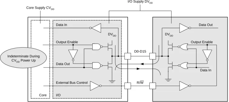
B. System-Level Bus Contention
Power supply sequencing may be required to prevent system-level bus contention, in which the bidirectional I/O pins of a DSP and external peripheral device oppose each other. Since the bus control logic originates in the core section of the DSP, powering I/O prior to the core may result in both the DSP and peripheral simultaneously configured as outputs. If the data values on each side are opposing, then the output drivers contend for control, as shown in Fig. 3.
Excessive current flows in one of the paths shown, depending on the opposing data-out patterns. The outputs contend for control and excessive current flows when the data values are opposing. This excessive current may damage the bidirectional I/O ports. Following the recommendation to power the core at the same time or before the I/O prevents undefined logic states on the bus control signals. [4]
III.SEQUENCING SCHEMES
There are three distinct schemes to power-up and power-down multi-rail power supplies: sequential, ratio-metric, and simultaneous [5]. The appropriate sequencing scheme is dependent on device requirements. The manufacturer's data sheet does not explicitly name which power sequencing scheme to implement, but rather outlines voltage and timing conditions that cannot be exceeded on power supply pins. Note that some devices allow out-of-bounds conditions for a short period of time. Using the pin conditions and the waveforms in the following section, a sequencing methodology can be chosen to meet the processor requirements.
Data In DVDD DVDD Data Out Output Enable Data In Output Enable Data Out
External Bus Control
I/O Core R/W D0-D15 Indeterminate During CVDD Power Up Core Supply CVDD I/O Supply DVDD
Dual Supply Voltage DSP Peripheral
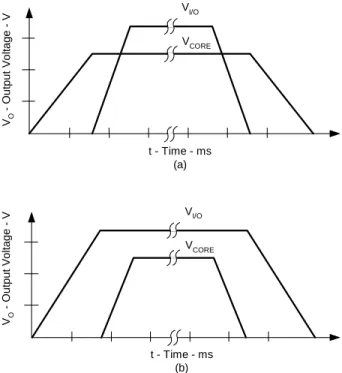
A. Sequential Sequencing
The sequential scheme of power supply sequencing is best described as one power supply ramping and settling to its final regulation voltage and then the second power supply ramping after a time delay. This method is used to initialize certain circuitry to a known state before activating another supply rail. An example applying the core supply rail prior to the I/O supply starting is shown in Fig. 4a.
t - Time - ms (a) VO - O u tput V o lt age V VI/O VCORE t - Time - ms (b) VO O u tput V o lt age V VI/O VCORE
Fig. 4. Sequential sequencing schemes.
The following is an excerpt from a footnote in a device specification with recommendations best suited to using sequential power supply sequencing:
“System-level concerns such as bus contention may require supply sequencing to be implemented. In this case, the core supply should be powered up at the same time as or prior to the I/O buffers and then powered down after the I/O buffers.” [6]
An alternative power supply sequence order would call for the I/O supply to power up first and the core supply to start after the I/O power supply reaches regulation, see Fig. 4b. In the particular example [7], this method meets the recommended power sequencing for the device as long as the delay time for the start up of the
core supply is less than 100 ms. As presented later in this topic, a typical hardware implementation employs an output voltage monitor to develop a power good (PG) signal for the first power supply, which then connects to the enable (EN) function of the second power supply.
B. Ratio-Metric Sequencing
For a dual power supply implementing ratio-metric sequencing, both power supply outputs ramp at the same time and in proportion until regulation is reached. Fig. 5a illustrates ratio-metric power sequencing where the core and I/O supply reach regulation at approximately the same instant. During power-up the core supply is a percentage of the I/O supply until regulation is reached. Similarly, during power-down the core is a specific percentage of the I/O supply voltage. Another example of ratio-metric sequencing may find the core supply voltage slightly greater than the I/O supply during the power-up and down, see Fig. 5b. In this particular case, to ensure the I/O buffers have valid inputs, the core rail is powered slightly before the I/O rail to eliminate problems with bus contention. [8]
t - Time - ms (a) VO - Out p ut V o lt ag e - V VI/O VCORE t - Time - ms (b) VO - Out p u t V o lt ag e - V VI/O VCORE
C. Simultaneous Sequencing
The simultaneous power sequencing method is similar to ratio-metric sequencing in that both power supply outputs ramp at the same time. However, in simultaneous sequencing, the objective is to minimize the voltage difference between the two supply rails during power up and down, as shown in Fig. 6, until regulation is reached for the core supply. This sequencing method is useful for devices that have “sneak paths” between supply pins or draw excessive current during startup if internal logic has not transitioned to a stable state. Reference [9] recommends simultaneous sequencing to minimize transient start-up currents.
t - Time - ms VO O u tp ut Vol tage V VI/O VCORE
Fig. 6. Simultaneous sequencing.
The following sections show many examples of power sequencing implemented with:
• Diodes
• Low-dropout (LDO) linear regulators
• Supply voltage supervisors (SVS)
• Power distribution switches
• Hot-swap controllers
• Microcontrollers
• Switch-mode controllers (power FETs external)
• Switch-mode converters (power FETs internal)
• Plug-in power modules
IV.SEQUENCING IMPLEMENTATIONS
ILLUSTRATED WITH LDOS
A. Diodes
Diodes are often used to facilitate sequencing requirements. Though diodes alone cannot achieve true sequential, ratio-metric or simultaneous sequencing, they can help maintain proper relation between various supply voltages.
Fig. 7 illustrates use of a Schottky diode to limit voltage differential between the core and I/O rail. The Schottky diode further reduces potential stress on devices by bootstrapping the I/O supply and shortening the delay between supply ramps. [5] I/O Voltage Regulator Core Voltage Regulator I/O DVDD Core CVDD DC Input
Fig. 7. Schottky diode limits voltage differential. Fig. 8 shows rectifiers in combination to help meet these microprocessor requirements:
• “VIN must not exceed VDDH by more than
2.5 V at any time, including during power-on reset.
• VDDH must not exceed VDD/VCCSYN by more
than 1.6 V at any time, including during power-on reset.
• VDD/VCCSYN must not exceed VDDH by more
than 0.4 V at any time, including during power-on reset.” [17] I/O Power Core/PLL Power 2.5 V (VDD/VCCSYN) 3.3 V (VDDH) DC Input
Fig. 8. Combination of diodes limits voltage differential.
“Note: There are internal diodes connected serially between VDDH and VDD, and vice-versa for ESD protection. If one of the voltages (VDD or VDDH) is applied and the other power pins are not driven, then the internal diodes pull up these pins. However, a problem could occur if one of the voltages (VDD or VDDH) is applied and the other voltage is forced to GND. In this case, the ESD diodes might be destroyed.”[17]
To achieve true sequential, ratio-metric or simultaneous sequencing, enlist the capabilities ofa wide range of active devices, as discussed in the following sections.
B. LDO Enable Via Supply Voltage Supervisor (SVS)
Sequential Sequencing
Fig. 9 shows an implementation of a supply voltage supervisor (SVS) to realize a sequential sequencing scenario. The load of this power supply is an FPGA which requires sequential sequencing. The power solution shown employs a 5-V input supply voltage rail. The core voltage is powered up first and, once the core voltage has ramped, the I/O voltage rail is enabled. Advantages of a linear regulator over a switch-mode approach typically include lower noise, reduced board space and cost. A key disadvantage is lower efficiency and, as a result, increased power dissipation.
VIN EN BYP VOUT GND IC1 TPS79618 C1 C3 R5 R1 LDO 1 A VDD RSTVDD SENSE RSTSENSE GND IC3 TPS3106K33 VIN = 5 V VIN EN BYP VOUT GND IC2 TPS78633 LDO 1.5 A C2 C6 C4 R2 C5 Q1 R3 R4 Core 1.8 V I/O 3.3 V R6
This solution is based on two LDOs, IC1 to supply core voltage and IC2 for the I/O voltage rail, along with an SVS, IC3. The dual SVS, with trip point threshold voltage of 2.941 V (typical), monitors the input voltage rail. Once the input voltage rail has reached the threshold of 2.941 V, the SVS reset output transitions from low to high impedance state after a delay of 130 ms, enabling LDO IC1. Once LDO IC1 is enabled, the core voltage ramps up towards its final value of 1.8 V. To ensure that the input voltage rail does not drop due to the high inrush current demand of the capacitor bank and the FPGA, a current-limiting circuit has been implemented. Without this current-limit circuit, the input voltage could potentially droop during the switch-on cycle. This current-limit circuitry, consisting of Q1, C4, R2, R6 and C5, provides smooth charging of the load during power-up.
Core voltage is monitored via a comparator incorporated in SVS IC3. Voltage divider R3 and R4 adjusts the threshold voltage to the particular needs of the application. In this case, it has been adjusted to a threshold voltage of 1.7 V. Once the core voltage reaches the threshold voltage, IC3 enables LDO IC2, which provides the I/O voltage to the system, and the I/O voltage ramps to its final value of 3.3 V.
The power-up and power-down waveforms of this implementation appear in Fig. 10.
t - Time - 50 ms/div (a) t - Time - 20 ms/div (b) 0.50 V/div V 0.50 V/div I/O VCORE VI/O VCORE
Simultaneous Sequencing
Some applications require either a specific slew rate or a maximum inrush current during power-up and power-down, which can be realized with the circuit in Fig. 11.
The power-up and power-down sequencing circuit employs network R3 and C2 to generate a ramp-up slope. This network is the slew rate reference for the output of the LDO during power-up and power-down. The operational amplifier compares the output voltage at its non-inverting input with the voltage applied to its inverting input. It then adjusts the output voltage to match the slew rate determined by the RC network. When ENABLE transitions low, Q1 is switched off, and R3 starts to charge C2 to the input voltage rail level. When VOUT reaches 2.5 V, set by R1 and R2, the voltage at the operational amplifier inverting input continues to rise, causing the operational amplifier output to decrease. This reverse-biases D1, thereby removing the power-up and power-down sequencing circuit from the feedback loop. R4 and C1 ensure a smooth voltage rise during power-up.
In this example, the output voltage set point can be calculated as follows:
− × = 2 1 1 REF OUT V V R R
where VREF = 1.224 V for the LDO shown.
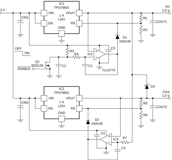
Fig. 12 features simultaneous sequencing circuitry that programs a required slew rate during power-up and power-down using IC2 as a tracking LDO.
The power-up and power-down sequencing circuit is using the same basic circuit as described above with programmable slope. In this example, the core voltage must track the I/O voltage during power-up and power-down. Additionally, the I/O voltage must be within 600 mV of the core voltage during power-up and power-down. If these conditions are violated, the processor could be damage due to forward-biasing of the substrate diode.
During power-up and power-down, IC4 provides active tracking to ensure that the voltage difference between I/O and core voltage is far less than the required 600 mV. Schottky diode D3 provides an additional level of protection.
During power-up, IC1’s output voltage increases with the applied slope ramp at the inverting node of IC3. Operational amplifier IC4 derives the ramp-up and ramp-down slope from the 2.5-V I/O output voltage rail. During power-up, the I/O voltage slowly increases, and this voltage is applied to the inverting node of IC4. The non-inverting node detects the core voltage, which is the output of linear regulator IC2. When the core voltage reaches 1.5 V, set by R5 and R6, the inverting input of operational amplifier IC4 continues to rise, causing the operational amplifier output to decrease. This reverse biases D2, removing the tracking circuit from the feedback loop. Fig. 13 displays power-up and power-down waveforms, respectively.
IC1 TPS79601 (1 A LDO) EN VIN FB VOUT GND CIN D1 1N4148 + C1 C3 R1 R2 COUT 3.3 V R4 C2 R3 IC3 I/O 2.5 V Q1 BSS138 ENABLE OFF ON TLV2770
IC1 TPS79601 EN VIN FB VOUT GND CIN1 D1 1N4148 + C1 C3 R1 R2 COUT1 IC2 TPS79601 EN VIN FB VOUT GND CIN2 D2 1N4148 + R5 R6 COUT2 3.3 V R4 C2 R3 IC3 C4 C5 R7 D3 Core 1.5 V I/O 2.5 V Q1 BSS138 ENABLE OFF ON TLV2770 1 A LDO 1 A LDO IC4
Fig. 12. Simultaneous sequencing with capacitor-programmable slew rate circuit.
t - Time - 50 ms/div (a) t - Time - 50 ms/div (b) 0.50 V/div 0.50 V/div VI/O VCORE VI/O VCORE
C. LDO and Power Distribution Switch
Sequential Sequencing
Some applications challenge the designer to apply core voltage prior to I/O voltage, even though the input source voltage is already at the I/O voltage level. A high-side power distribution switch can be used to disable the I/O supply until the core voltage is powered up and stable. Fig. 14
shows a sequential power supply sequencing implementation using the TPS2150, which integrates a high-side power switch with an LDO.
The TPS2150 uses the power good function of the LDO to enable the power switch, resulting in the power-up waveforms of Fig. 15a. The power switch and LDO feature pull down MOSFETs to discharge the bulk capacitance when the devices are disabled (Fig. 15b).
250 mA LDO Driver Charge Pump 10 µF 10 µF 3.3 V 10 kΩ 4.7 kΩ 10 µF 2.5 V 3.3 V TPS2150 SW_PLDN SW_OUT LDO_PG LDO_PLDN ADJ LDO_OUT SW_IN LDO_IN 3.3 V SW_EN LDO_EN REF
Fig. 14. Sequencing with combination LDO/high-side switch (core then I/O).
t - Time - 200 µs/div (a) t - Time - 1 ms/div (b) PG VI/O VCORE PG VI/O VCORE PG 2 V/div VCORE 1 V/div VI/O 1 V/div PG 2 V/div VCORE 1 V/div VI/O 1 V/div
Fig. 16 implements the opposite configuration, in which the I/O voltage is applied before the core at turn-on. Corresponding waveforms are shown in Fig. 17.
250 mA LDO Driver Charge Pump 10 µF 10 µF 3.3 V 10 kΩ 4.7 kΩ 10 µF 2.5 V 3.3 V 3.3 V TPS2150 SW_PLDN SW_OUT SW_PG LDO_PLDN ADJ LDO_OUT LDO_EN SW_IN SW_EN LDO_IN
Fig. 16. Sequential sequencing (I/O then core).
t - Time - 500 µs/div (a) t - Time - 1 ms/div (b) PG VI/O VCORE PG VI/O VCORE PG 2 V/div VCORE 1 V/div VI/O 1 V/div PG 2 V/div VCORE 1 V/div VI/O 1 V/div
D. Hot-Swap Control
Simultaneous Sequencing
Another method to up and power-down with minimum voltage difference between the power supply rails is to use MOSFETs between the supply and load. Fig. 18 shows a simplified schematic using two MOSFETs and a TPS2331 hot swap controller to provide simultaneous start-up sequencing. By driving the gates of the MOSFETs with the same gate driver, the power supply rails effectively ramp together (Fig. 19a). The TPS2331 features an integrated pull-down transistor to discharge the bulk output capacitors, see Fig. 19b. The Schottky diode clamps the core supply during power-down.
Logic UVLO Charge Pump Clamp EN IN GATE DISCH GND 1 kΩ 1 kΩ 10 µF 3.3 V 150 µF 150 µF 10 µF 2.5 V Core I/O SI4410 SI4410 6800 pF TPS2331
Fig. 18. Simultaneous sequencing with hot-swap controller. t - Time - 500 µs/div (a) 1.0 V/div VIO VCORE t - Time - 20 ms/div (b) 1.0 V/div VIO VCORE
Fig. 19. Power-up (a) and power-down (b) waveforms for circuit of Fig. 18.
E. Microcontroller
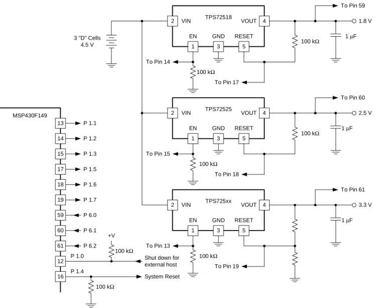
Microcontrollers are among the most versatile devices available for sequencing. If the power supplies to be controlled feature enable pins, then controlling them is a simple matter of using general purpose input and output (GPIO) lines. If the enable function is not available, an in-line MOSFET or power distribution switch can be used to control the power supply, either with a GPIO or PWM signal.
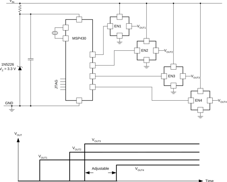
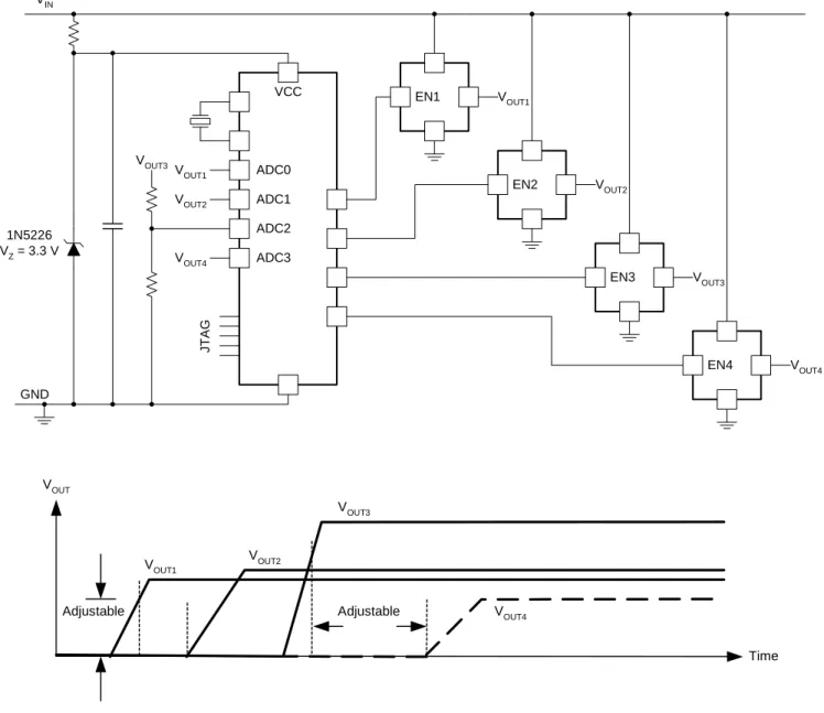
Use of a microcontroller is illustrated with the MSP430, a 16-bit RISC processor featuring several analog peripherals and a JTAG interface. The circuit of Fig. 20 uses the TPS725xx family of LDOs to provide 3.3 V, 2.5 V and 1.8 V from an input DC source. These LDOs have an enable pin and reset function. This circuit can easily be expanded to any number of voltage rails. The MSP430 monitors a control variable to determine when each rail should be activated. For power sequencing applications, the two most commonly controlled variables are time and voltage.
3 1 2 4 5 TPS72518 GND EN VIN VOUT RESET 100 kΩ 100 kΩ 1 µF 3 1 2 4 5 TPS72525 GND EN VIN VOUT RESET 100 kΩ 100 kΩ 1 µF 3 1 2 4 5 TPS725xx GND EN VIN VOUT RESET 100 kΩ 1 µF To Pin 61 To Pin 60 To Pin 59 To Pin 17 To Pin 18 To Pin 19 To Pin 13 To Pin 15 To Pin 14 13 14 15 17 18 19 59 60 61 12 16 MSP430F149 100 kΩ P 6.2 P 6.1 P 6.0 P 1.7 P 1.6 P 1.5 P 1.3 P 1.2 P 1.1 P 1.0 P 1.4 100 kΩ System Reset Shut down for external host 3 "D" Cells 4.5 V +V 3.3 V 2.5 V 1.8 V
Sequential Sequencing
When time is the control variable the first rail is enabled then, at a specific time thereafter, the next rail is enabled. Some time after that the next rail is enabled and so on, until all rails have been enabled. The MSP430 provides the timing sequence and the control signals to turn on the power supplies (Fig. 21).
If voltage is the control variable, then the first voltage rail is activated and its rise is monitored via an analog-to-digital converter (ADC). When the first voltage rail has reached a specific voltage level, the next voltage rail is enabled and its rise is monitored until it has reached a specified voltage level, at which point the next voltage rail is enabled and monitored. This continues until all voltage rails have been enabled (Fig. 22). When using voltage as the control variable, either a GPIO or PWM signal can be used as the enable signal, depending on whether rail tracking is required. Of course, a combination of voltage and timing control can also be used.
VOUT1 EN1 VOUT2 EN2 VOUT3 EN3 VOUT4 EN4 JTAG MSP430 VIN GND 1N5226 VZ = 3.3 V VOUT Time Adjustable VOUT1 VOUT2 VOUT3 VOUT4
Once the MSP430 has turned on all the voltage rails and applied the system reset, it enters the monitor mode. It continually checks the output voltages, via the reset or output pins, depending on whether time or voltage is the control variable. If a fault occurs, the MSP430 enters an error routine. The most obvious fault would be the loss of a voltage rail, but other faults such as over- or under-voltage could also be monitored. The actions taken in the error
routine are completely application-dependent. The simplest action is to power down all rails, but programmability offers the user complete control.
Power-down sequencing can be just the opposite of the power up sequence, or any sequence required to meet system demands. One addition to the power-down sequence could be turning on dummy loads to discharge the output filter capacitors. [16] VOUT1 EN1 VOUT2 EN2 VOUT3 EN3 VOUT4 EN4 ADC3 ADC2 ADC1 ADC0 VOUT3 VOUT4 VOUT2 VOUT1 VCC VIN GND 1N5226 VZ = 3.3 V JTAG VOUT Time Adjustable Adjustable VOUT1 VOUT2 VOUT3 VOUT4
V.SEQUENCING WITH SWITCH-MODE
CONTROLLERS,CONVERTERS AND MODULES
A. Pre-Bias Start-Up and Synchronous Rectifier
Many switch-mode power stages employ synchronous rectification to improve efficiency, as illustrated by the simplified synchronous buck converter shown in Fig. 23. In this example, VIO comes up first, and applies core voltage through the series diodes before the core’s converter is enabled. Defining this as a pre-bias condition, in which voltage is applied at the converter output before the converter is enabled. When the converter’s PWM controller is enabled, it soft-starts the high-side FET, and its duty cycle (D) ramps gradually from zero to that required for regulation. However, if during soft-start the synchronous rectifier (SR) FET is on when the high-side FET is off (SR FET duty cycle = 1-D), the SR sinks current from the output (through the inductor), tending to cause both the core and I/O voltages to drop. It is for this reason that PWM controllers with pre-bias start-up have been introduced, which disable SR drive during start-up. Until drive to the SR is enabled, inductor current flows through the parasitic body diode of the SR FET rather than through the channel. Once the soft-start time is complete, drive to the SR is enabled.
VCORE VIO
PWM
Fig. 23. Example of pre-bias condition.
The need for synchronous converters with pre-bias start-up also arises when using a sequential power-up technique with some ASICs, in which a leakage path within the device causes some I/O voltage to appear on the core voltage before the core converter is enabled. Fig. 24 uses a PTH series power module for illustration. The PTH power modules incorporate synchronous rectification, so can sink current under normal operating conditions, but the 3.3-V and 5-V input versions do not do so during power-up, or whenever the module is turned off via the Inhibit pin. In Fig. 24, module U1 (PTH05020W) produces 2.5 V for the core.
1,7 3 8 5 2 10 9 6 4 PTH05020W R2 2.21 kΩ COUT 330 µF CIN 330 µF VCORE VCCIO VIN = 3.3 V IO ASIC VO = 2.5 V + + GND INHIBIT VIN TRACK VO VADJ SENSE +
Fig. 25 shows the waveforms of the circuit after input power is applied. It shows VO rising
along with VIN once VIN forward-biases the leakage path within the ASIC. Note that output current (IO) is negligible until VO rises above the
pre-bias voltage (point A). From hereon, the waveform of IO exhibits a positive output current.
[19] t - Time - 5 ms/div IO (5 A/div) VO (1 V/div) VIN (1 V/div) A
Fig. 25. Power-up waveforms with pre-bias.
B. DC-DC Controllers
Ratio-Metric Sequencing
In ratio-metric sequencing, multiple output power rails start ramping at the same time and in proportion. This function can be accomplished with multiple controllers sharing a common soft-start capacitor. The solution in Fig. 26 (waveforms in Fig. 27) is based on two TPS40051 synchronous buck controllers with a wide input voltage range of 8 V to 40 V. These controllers drive synchronous rectifiers and feature feed-forward voltage-mode control. In this example, I/O voltage is 3.3 V and core voltage is 1.8 V.
Soft-start is programmed by charging external capacitor C2 via an incorporated current source of 2.3 µA. The voltage rise on C2 is then fed into a separate non-inverting input to the error amplifier (in addition to the feedback voltage and the 700-mV reference voltage). Once voltage on C2 exceeds 700 mV, the internal reference voltage is used to establish regulation. To ensure a controlled ramp of the output voltage, the soft-start time should be greater than the output inductor and output capacitor time constant.
So, in this example,
C13 L1 2
tSTART≥
π
× (seconds)and the soft-start capacitance calculates as:
START t V A C × × = 7 . 0 3 . 2 2 2
µ
(Farads),since the current feeding the soft-start capacitor is 2.3 µA per controller. [20]
IC1 TPS40051 SYNC SGND SS/SD VFB COMP HDRV BP10 LDRV PGND BOOST SW VIN ILIM BPS RT KFF R13 C10 R9 C8 R8 C17 C9 D1 C12 R10 L1 C13 C14 Q1a Q1b C7 R5 R12 C16 C6 C11 R2 C1 R1 R4 C4 C3 R7 C5 R6 R3 D2 3.3 V IC2 TPS40051 SYNC SGND SS/SD VFB COMP HDRV BP10 LDRV PGND BOOST SW VIN ILIM BPS RT KFF R13b C10b R9b C8b R8b C17b C9b D1b C12b R10b L2b C13b C14b Q2a Q2b C7b R5b R12b C16b C6b C11b R2b C1b R1b R4b C4b C3b R7b C5b R6b R3b D2b 1.8 V C2
Fig. 26. Ratio-metric sequencing with common soft-start capacitor.
t - Time -200 µs/div (a) t - Time - 0.2 s/div (b) 0.50 V/div V 0.50 V/div I/O VCORE VI/O VCORE
C. DC-DC Converters
Simultaneous Sequencing
As previously mentioned, the objective of simultaneous sequencing is to minimize the potential difference between voltage rails as they ramp. Fig. 28 illustrates such an implementation using switcher with integrated FET (SWIFT) converters that integrate both high-side and synchronous rectifier FETs. IC1 provides I/O voltage of 3.3 V, while IC2 provides core voltage of 1.5 V. The converters share one soft-start capacitor (C14) to ensure the outputs ramp at the same slope. Note that these are voltage-mode controlled converters. IC2 acts as master controller. Its output voltage is programmed at 1.5 V via voltage divider R14 and R12. Additionally, its power-good (PGOOD) comparator is used as a master flag to release the voltage divider of IC1.
During power up (Fig. 29a), both converter output voltages rise with the ramp of the soft-start capacitor to an output voltage of 1.5 V. This is due to voltage dividers R14 and R12 at IC2, and R8 and R3 at IC1. During power-up, the power good (PGOOD) pin of IC2 is active low, holding Q1 off so that the output voltages track during power up until IC2 reaches 90% of its final value. Once IC2 detects an output voltage level of 90% or greater, PGOOD goes high impedance, and pull-up resistor R4 drives the gate of Q1 on via RC network R5 and C11. Once the gate threshold voltage of Q1 reaches 1.6V (typical), it starts to conduct and switches R6 in parallel to R3. This parallel combination changes the output voltage set point of IC1 to program 3.3-V output. IC2 TPS54610 VIN PGOOD RT VBIAS SS PH BOOT VSENSE COMP GND IC1 TPS54310 VIN RT VBIAS SYNC SS PH BOOT VSENSE COMP GND R1 C5 R9 D1 C13 R4 R10 C15 C14 C2 C1 VIN 5 V R2 C10 C9 R8 C12 R7 R3 R6 C11 R5 C7 C8 L1 C6 R11 C17 C16 R14 C18 R13 R12 C20 C21 L2 C19 VIO 3.3 V IMAX 3 A Core 1.5 V IMAX 6 A Q1
t - Time - 2.0 ms/div (a) t - Time - 0.1 s/div (b) 0.50 V/div V 0.50 V/div I/O V I/O VCORE VCORE
Fig. 29. Power-up (a) and power-down (b) waveforms for Fig. 28.
In this implementation, a general purpose BSS138 FET is used with a typical threshold voltage of VGSth = 1.6 V. This FET features
RDS(on) < 10 Ω (negligible compared to the values
of R3 and R6), so does not affect the calculated output voltage set point value.
The set point resistor values can be calculated as follows:
A. Equation for VCORE
REF CORE REF V V R V R − × = 8 3 VCORE = 1.5 V, VREF = 0.891 V Choose R8= 27.4 kΩ then R3 = 40.2 kΩ
B. Equation for VI/O
REF O I REF X V V R V R − × = / 8 where RX is R3 || R6 VI/O = 3.3 V so RX = 10.22 kΩ C. Equation for R6 1/RX = 1/ R3+ 1/ R6 so, 3 / 1 / 1 1 6 R R R X − = R6= 13.7 kΩ
PGOOD of IC2 transitions low when VCORE
falls under 90% of its initial value during power-down (Fig. 29b). This discharges C11 and the gate of Q1 via R5. Once the gate of Q1 falls below its threshold voltage level (1.6 V typical), R6 is removed from the feedback divider. Thus IC1’s output voltage set point drops to 1.5 V and the I/O voltage ramps down along with the core voltage. Note during power-down the voltages do not track each other due to differing output capacitor energy storage and load levels. The tracking version of the SWIFT converters can be used to address this issue.
A noteworthy feature of this implementation is that the converters are running at the same switching frequency. IC2 is the master device programmed to a switching frequency of 700 kHz. IC1 starts at a lower initial switching frequency of roughly 630 kHz, 10% below the switching frequency of IC2. Once IC2 begins to operate, it synchronizes IC1 via the SYNC pin. Diode D1 limits negative voltage spike amplitude at the SYNC input.
Sequential Sequencing
Fig. 30 shows a dual power supply design with sequential power-up using the TPS54350 dc/dc converter. The circuit uses the power good function of the I/O supply to activate the enable of the core supply. Once the I/O supply is up and stable, the power good pin (PWRGD) transitions from active low to high impedance (see Fig. 31). The TPS54350 has an internal pull-up current source on the enable (ENA) pin, so an external
pull-up resistor is not required to enable the core supply. As discussed in the last section, the challenge with using this power good and enable technique is the power-down sequence. It is preferred to power down the supply rails in the reverse order of power up. Because of supply loading and the disabling of the I/O supply and core supply at the same time, this order is not guaranteed. 1 2 3 4 5 6 7 8 U1 TPS54350PWP 16 15 14 13 12 11 10 9 VIN VIN UVLO PWRGD RT SYNC ENA COMP BOOT PH PH LSG VBIAS PGND AGND VSENSE PWRPD R3 768 Ω C7 1800 pF R1 180 kΩ C8 33 nF R9 0 Ω C4 1.0 µF C3 0.1 µF 2 3 8 7 1 6 5 4 FDR6674A Q1 R10 4.7 Ω C11 3300 pF L1 10 µH 2 1 C2 100 µF + 1 2 0.1 C10µF VOUT 3.3 V R3 768 Ω R13 768 Ω C9 10 µF C1 47 µF + VIN 6 V to 13 V C6 82 nF R5 137 Ω 1 2 3 4 5 6 7 8 U2 TPS54350PWP 16 15 14 13 12 11 10 9 VIN VIN UVLO PWRGD RT SYNC ENA COMP BOOT PH PH LSG VBIAS PGND AGND VSENSE PWRPD R6 768 Ω C17 1800 pF R12 1.8 kΩ C12 33 nF R14 0 Ω C16 1.0 µF C5 0.1 µF 2 3 8 7 1 6 5 4 FDR6674A Q2 R15 4.7 Ω C20 3300 pF L2 10 µH 2 1 C18 100 µF + 1 2 0.1 C13µF VOUT 1.8 V C15 10 µF C14 47 µF + C19 82 nF R11 137 Ω R16 374 kΩ Pull Up 3.3 V or 5 V Power Good 3.3 V Power Good 1.5 V R2 374 Ω R7 976 Ω
t - Time - 2.0 ms/div VOUT2 2.0 V/div PWRGD 2.0 V/div VOUT1 2.0 V/div VIN 10.0 V/div
Fig. 31. Power-up waveforms of Fig. 30.
Another technique to implement sequential sequencing is implemented by connecting the power good function to the TRACKIN pin of a TPS54680 Sequencing SWIFT converter using resistors and a capacitor (Fig. 32) [10]. The TPS54680 was designed for applications that have critical power supply sequencing requirements. The device has a TRACKIN pin to facilitate the various sequencing methods. The TRACKIN pin is the input to an analog multiplexer that compares a 0.891-V internal voltage reference to the voltage on the TRACKIN pin, and connects the lower of the voltages to the non-inverting node of the error amplifier. When the TRACKIN pin voltage is lower than the internal voltage reference, the TRACKIN pin voltage is effectively the reference for the power supply. The power-up and power-down waveforms are shown Fig. 33.
+ Analog Multiplexer 6.04 kΩ Error Amp COMP VSENSE 0.891 V Reference TRACKIN Input Supply Core Supply TPS54680 PWRGD TPS54610 10 kΩ 0.1 µF
t - Time - 1.0 ms/div VCORE 1.0 V/div VIO 1.0 V/div VIO RL = 1 kΩ VCORE RL = 1 kΩ t - Time - 20.0 ms/div VCORE 1.0 V/div VIO 1.0 V/div VIO RL = 1 kΩ VCORE RL = 1 kΩ
Fig. 33. Power-up (a) and power-down (b) waveforms of Fig. 32.
As shown in Fig. 33a, the 3.3-V I/O supply ramps first. When the I/O supply reaches its final 3.3-V steady state value, the open drain output of the PWRGD pin releases the TRACKIN pin, and the core supply rises at the rate of the RC time constant. The 0.1-µF capacitor is used to minimize the inrush current during startup of the core supply. The PWRGD pin asserts, pulling the TRACKIN pin low, when the SSENA pin is pulled low on the TPS54610 or when the I/O voltage is below 90% of the desired regulated voltage. Ideally, the I/O and core supplies power down in opposite order of power-up. If there is no load or a light load on the core when the I/O rail powers down, the TPS54680 device has the ability to sink current and transfers the energy stored in the output capacitor to the input capacitor. Fig. 33b shows power-down with 1-kΩ loads on both outputs.
Ratio-Metric Sequencing 120 pF 4.22 kΩ 2200 pF + Analog Multiplexer 9.76 kΩ 3.74 kΩ 10 kΩ 10 kΩ 820 pF 511 Ω Error Amp COMP VSENSE 0.891 V Reference TRACKIN I/O Supply Core Supply TPS54680
Fig. 34 Ratio-metric sequencing with TPS54680 track input.
The analog multiplexer on the TPS54680 can also provide ratio-metric power sequencing by setting the divider ratio on the TRACKIN pin to a different value than that of the feedback compensation. Fig. 34 shows a simplified schematic with the TRACKIN voltage divider set to program lower voltage than the feedback divider, resulting in the core powering-up and down in proportion to the I/O voltage. The waveforms for the core and I/O supplies are shown in Fig. 35a and 35b.
t - Time - 1.0 ms/div (a) VCORE 1.0 V/div VI/O 1.0 V/div VI/O RL = 1 kΩ VCORE RL = 1 kΩ t - Time - 50.0 ms/div (b) VCORE 1.0 V/div VI/O 1.0 V/div VI/O RL = 1 kΩ VCORE RL = 1 kΩ
Fig. 35. Power-up (a) and power-down (b) waveforms of Fig. 34.
If the core supply must power up slightly before the I/O supply, the TRACKIN voltage divider ratio should be set to program higher voltage than that of the feedback divider (sample schematic and waveforms in Fig. 36 and 37). For an equation on the selection of the TRACKIN resistors see reference [10].
120 pF 4.22 kΩ 2200 pF + Analog Multiplexer 9.76 kΩ 26.1 kΩ 10 kΩ 10 kΩ 820 pF 511 Ω Error Amp COMP VSENSE 0.891 V Reference TRACKIN I/O Supply Core Supply TPS54680
t - Time - 1.0 ms/div (a) VCORE 1.0 V/div VI/O 1.0 V/div VI/O RL = 1 kΩ VCORE RL = 1 kΩ t - Time - 50.0 ms/div (b) VCORE 1.0 V/div VI/O 1.0 V/div VI/O RL = 1 kΩ VCORE RL = 1 kΩ
Fig. 37. Power-up (a) and power-down (b) waveforms of Fig. 36.
Simultaneous Sequencing
To minimize voltage differences between supply rails during power-up and down, the TPS54680 can be configured for simultaneous sequencing as shown in Fig. 38. By selecting the TRACKIN voltage divider to have the same ratio as the voltage divider in the feedback compensation loop, the core and I/O supplies power up and down with waveforms similar to Fig. 39. As before, the outputs of the regulators are loaded with 1-kΩ resistors. It can be observed from the waveforms that the voltage difference between the rails is minimal during power down. If the I/O supply is heavily loaded and the core supply is lightly loaded during power down, there may be a voltage difference between the rails. This is because the core supply cannot sink current as fast as the I/O supply is falling. This can be countered by adding more bulk capacitance on the I/O output.
120 pF 4.22 kΩ 2200 pF + Analog Multiplexer 9.76 kΩ 9.76 kΩ 10 kΩ 10 kΩ 820 pF 511 Ω Error Amp COMP VSENSE 0.891 V Reference TRACKIN I/O Supply Core Supply TPS54680
Fig. 38. Simultaneous sequencing with TPS54680 track input.
t - Time - 1.0 ms/div (a) VCORE 1.0 V/div VI/O 1.0 V/div VI/O RL = 1 kΩ VCORE RL = 1 kΩ t - Time - 50.0 ms/div (b) VCORE 1.0 V/div VI/O 1.0 V/div VI/O RL = 1 kΩ VCORE RL = 1 kΩ
Fig. 39. Power-up (a) and power-down (b) waveforms of Fig. 38.
VI.SUMMARY
Design of a multi-rail power system often involves much more than simply converting input voltages to output voltages and currents. As has been discussed, the power-up and power-down sequencing of these voltages can significantly impact proper system operation and reliability. Three distinct power sequencing schemes have been defined (sequential, ratio-metric and simultaneous) and implementations have been illustrated with a breadth of power devices, ranging from LDOs to PWM controllers and converters to power modules. We’ve also enlisted control and monitoring devices including supply voltage supervisors and a microcontroller. Of course, these devices can be applied in combination as needed to meet the power sequencing requirements of any given system.
VII.ACKNOWLEDGEMENTS
The authors wish to thank Joe DiBartolomeo and Chris Thornton for their generous contributions to this work.
REFERENCES
[1] Gray, Paul and Meyer, Robert Analysis and Design of Analog Integrated Circuits third edition, John Wiley & Sons, Inc., New York, 1993, Chapter 2
[2] O’Connor, Chris and Weiss, Gary, Looking for Latch-up?, Test & Measurement World, pages 31-34, September 2003
[3] XC9500 CPLD Power Sequencing, Application Note, (XAPP110) Version 1.0, February 16, 1998 Xilinx
[4] Power Supply Sequencing Solutions for Dual Supply Voltage DSPs, (SLVA073A), Texas Instruments
[5] Rush, Brian, Power Supply Sequencing for Low Voltage Processors, EDN, September 1, 2000, pp. 115-118
[6] TMS320VC5402 Data Sheet, (SPRS079E), Texas Instruments
[7] MPC8260EC/D (HiP3) Hardware Specification, Motorola, page 5, May 5, 2002
[8] TMS320VC6203B Data Sheet,
(SPRS086K), Texas Instruments
[9] Power Up Behavior of ProASIC 500 k
Ω
Devices, Application Note, Actel Corporation[10] Sequencing with TPS54x80 and TPS54x73 DC/DC Converters, (SLVA007), Texas Instruments
[11] TPS2140 Data Sheet, Texas Instruments (SLVS399)
[12] C.S. Mittlere, Active Inrush Current Limiting Using MOSFETs, Application Note, (AN1542), Motorola
[13] Power Management Reference Guide for Xilinx®, Texas Instruments (SLPB008) [14] Wide Range Input TPS40051 Converter
Delivers 5 V at 2 Amps, Application Note, (SLUU163), Texas Instruments
[15] Circuit Manages Power-Up Sequencing, Martin Galinski, Micrel Semiconductor, EDN October 2002
[16] DiBartolomeo, Joe, Microcontroller Directs Supply Sequencing and Control, EDN, May 29, 2003, pp. 73-74
[17] Minimum MPC8260 PowerQUICC II System Configuration, (AN1819), Motorola. [18] Chris Thornton, Auto-TrackTM Voltage
Sequencing Simplifies Power-Up and Power-Down, Analog Applications Journal, (SLYT047A), Texas Instruments
[19] Chris Thornton, New Power Modules Include Supply Voltage Sequencing and Margin Test Capabilities, ChipCenter's Analog Avenue September 1, 2003
[20] TPS40051 Data Sheet, (SLUS540), Texas Instruments
APPENDIX A
LIST OF MATERIALS FOR FIG.9.
Reference Count Description Manufacturer Part Number
IC1 1 LDO, 1.80 V, 1.0 A TI TPS79618KTT
IC2 1 LDO, 3.3 V, 1.5 A TI TPS78633KTT
IC3 1 SVS TI TPS3106K33
C1, C2 2 Capacitor, POSCAP, 100 µF, 10 V, 55 mΩ, 20%,
7343 Sanyo 10TPB100M
C3, C6 2 Capacitor, ceramic, 10 µF, 6.3 V, X5R, 20%, 1210 MuRata GRM31CR60J106KC01
C4 1 Capacitor, ceramic, 100 nF Std Std C5 1 Capacitor, ceramic, 0.47 µF Std Std R1, R5 2 Resistor, chip, 100 kΩ, 1/16 W, 1%, 805 Std Std R2 1 Resistor, chip, 7.5 Ω, 1/16 W, 1%, 805 Std Std R3 1 Resistor, chip, 23.2 kΩ, 1/16 W, 1%, 805 Std Std R4 1 Resistor, chip, 11 kΩ, 1/16 W, 1%, 805 Std Std R6 1 Resistor, chip, 100 Ω, 1/16 W, 1%, 805 Std Std Q1 1 P-channel, FET, -12 V, -3 A, SOT-23. Vishay Si2333DS
APPENDIX B
LIST OF MATERIALS FOR FIG.12.
Reference Count Description Manufacturer Part Number
IC1, IC2 2
IC, LDO Regulator, Available in 1.80-V, 2.5-V, 2.8-V, 3-V, 3.3-V and Adjustable , 1 A, ultralow noise, high PSRR, T0-263
TI TPS79601KTT
IC3, IC4 2 Single 2.7-V High-Slew-Rate Rail-to-Rail Output
Operational Amplifier w/Shutdown , SOT-23 TI TLV2770CDGKR
CIN1, CIN2 2 Capacitor, POSCAP, 100 µF, 10 V, 55 mΩ, 20%,
805 Murata GRM21BR60J225KC01
COUT1,
COUT2 2 Capacitor, ceramic, 10 µF, 6.3 V, X5R, 20%, 805 Murata GRM21BR60J225KC01 Q1 1 BSS 138, N-channel enhancement, SOT-23 Fairchild
Semiconductor BSS128 D2 2 Small signal diode, LL-34 Fairchild
Semiconductor 1N4148 D3 1 Shottky barrier rectifiers, DPAK On
Semi-conductor MBRD320-D C1, C2, C3, C4, C5 5 Capacitor, ceramic, 100 nF, X7R, 10% Std Std R1, R5 2 Resistor, chip, 31.6 kΩ, 1/16 W, 1%, 805 Std Std R2 1 Resistor, chip, 30.1 kΩ, 1/16 W, 1%, 805 Std Std R3 1 Resistor, chip, 300 kΩ, 1/16 W, 1%, 805 Std Std R4, R7 2 Resistor, chip, 4.99 kΩ, 1/16 W, 1%, 805 Std Std R6 1 Resistor, chip, 140 kΩ, 1/16 W, 1%, 805 Std Std
APPENDIX C
LIST OF MATERIALS FOR FIG.26.
Reference Count Description Manufacturer Part Number
C1, C7, C10, C1b, C7b,
C10b 6 Capacitor, ceramic, 0.1 µF, 25 V, X7R, 10%, 805 Vishay VJ0805Y104KXXAT C11, C11b 2 Capacitor, aluminum, 100 µF, 63 V, 20% Panasonic EEVFK1J101P
C13, C13b 2 Capacitor, POSCAP, 330 µF, 6.3 V, 10 mΩ, 20%,
7343D Sanyo 6TPD330M
C14, C14b 2 Capacitor, ceramic, 1 µF, 16 V, X5R, 20%, 805 TDK C2012X5R1C105KT C16, C16b 2 Capacitor, ceramic, 470 pF, 50 V, X5R, 20%, 805 Vishay VJ0805Y471KXAAT
C2, C12, C17, C2b,
C12b, C17b 6 Capacitor, ceramic, 2.2 nF, 50 V, X7R, 10%, 805 Vishay VJ0805Y222KXAAT C3, C3b 2 Capacitor, ceramic, 82 pF, 50 V, NPO, 5%, 805 Panasonic VJ0805A820KXAAT C4, C4b 2 Capacitor, ceramic, 2.7 nF, 50 V, X7R, 10%, 805 Vishay VJ0805Y272KXAAT C5, C5b 2 Capacitor, ceramic, 10 nF, 50 V, X7R, 10%, 805 Vishay VJ0805Y103KXAAT
C6, C6b 2 Capacitor, ceramic, 1.5 µF, 50 V, X7R, 10%, 1210 TDK C3225X7R1H155KT C8, C8b 2 Capacitor, ceramic, 100 pF, 50 V, X7R, 10%, 805 Vishay VJ0805A101KXAAT
C9, C9b 2 Capacitor, ceramic, 1 µF, 16 V, X7R, 10%, 805 Vishay C2012X5R1C105KT D1, D1b 2 Diode, schottky, 1 A, 60 V, 45600 IR 10BQ060
D2, D2b 2 Diode, switching, 10 mA, 85 V, 350 mW, SOT-23 Vishay-Liteon BAS16
L1, L2b 2 Inductor, SMT, 22 µH, 4.5 A, 34 mΩ, 0.85 ξ 0.59 Coiltronics UP4B-220 Q1, Q2 2 MOSFET, dual N-channel, 60 V, 3.8 A, 55
mΩ, SO-8 Siliconix Si946EY
R1, R1b 2 Resistor, chip, 1 kΩ, 1/10 W, 1%, 805 Std Std R10, R10b 2 Resistor, chip, 4.7 Ω, 1 W, 5%, 2512 Std Std R11, R11b 2 Resistor, chip, 20 Ω, 1/10 W, 1%, 805 Std Std R12, R12b 2 Resistor, chip, 243 kΩ, 1/10 W, 1%, 805 Std Std R13, R13b 2 Resistor, chip, 8.2 Ω, 1/10 W, 5%, 805 Std Std R2, R2b 2 Resistor, chip, 165 kΩ, 1/10 W, 1%, 805 Std Std R3 1 Resistor, chip, 2.1 kΩ, 1/10 W, 1%, 805 Std Std R3b 1 Resistor, chip, 4.99 kΩ, 1/10 W, 1%, 805 Std Std R4, R4b 2 Resistor, chip, 30.1 kΩ, 1/10 W, 1%, 805 Std Std R5, R5b 2 Resistor, chip, 71.5 kΩ, 1/10 W, 1%, 805 Std Std R6, R6b 2 Resistor, chip, 7.87 kΩ, 1/10 W, 1%, 805 Std Std R7, R7b 2 Resistor, chip, 100 Ω, 1/10 W, 1%, 805 Std Std R8, R8b 2 Resistor, chip, 3.3 Ω, 1/10 W, 5%, 805 Std Std R9, R9b 2 Resistor, chip, 20 kΩ, 1/10 W, 1%, 805 Std Std IC1, IC2 2 Wide Input Synchronous Buck Controller TI TPS40051PWP
APPENDIXD
LIST OF MATERIALS FOR FIG.28
References Count Description Manufacturer Part Number
C1 1 Capacitor, aluminum, 470 µF, 6.3 V, 20%, 140CLH
series, 1010 BC Components 2222 140 95301 C2, C4 2 Capacitor, ceramic, 10 µF, 6.3 V, X5R, 20%, 1206 muRata GRM319 R6 0J 106K C7, C8,
C20, C21 4 Capacitor, ceramic, 47 µF, 6.3 V, X5R, 20%, 1210 muRata GRM42-2 X5R 476K C3, C14 2 Capacitor, ceramic, 39 nF, X7R, 10%, 603 Std Std C6, C19 2 Capacitor, ceramic, 47 nF, X7R, 10%, 603 Std Std C9, C11 2 Capacitor, ceramic, 470 pF, X7R, 10%, 603 Std Std C10 1 Capacitor, ceramic, 6.8 nF, X7R, 10%, 603 Std Std C12 1 Capacitor, ceramic, 1.8 nF, X7R, 10%, 603 Std Std C13 1 Capacitor, ceramic, 56 pF, X7R, 10%, 603 Std Std C5, C15 2 Capacitor, ceramic, 100 nF, X7R, 10%, 603 Std Std C16 1 Capacitor, ceramic, 1.5 nF, X7R, 10%, 603 Std Std C17 1 Capacitor, ceramic, 18 nF, X7R, 10%, 603 Std Std C18 1 Capacitor, ceramic, 5.6 nF, X7R, 10%, 603 Std Std R1 1 Resistor, chip, 76.8 kΩ, 1/16 W, 1%, 603 Std Std R2 1 Resistor, chip, 3.83 kΩ, 1/16 W, 1%, 603 Std Std R3 1 Resistor, chip, 40.2 kΩ, 1/16 W, 1%, 603 Std Std R4, R5 2 Resistor, chip, 330 kΩ, 1/16 W, 1%, 603 Std Std R6 1 Resistor, chip, 13.7 kΩ, 1/16 W, 1%, 603 Std Std R7 1 Resistor, chip, 105 Ω, 1/16 W, 1%, 603 Std Std R8 1 Resistor, chip, 27.4 kΩ, 1/16 W, 1%, 603 Std Std R9 1 Resistor, chip, 1 kΩ, 1/16 W, 1%, 603 Std Std R10 1 Resistor, chip, 71.5 kΩ, 1/16 W, 1%, 603 Std Std R11 1 Resistor, chip, 1.43 kΩ, 1/16 W, 1%, 603 Std Std R12 1 Resistor, chip, 14.7 kΩ, 1/16 W, 1%, 603 Std Std R13 1 Resistor, chip, 33.2 Ω, 1/16 W, 1%, 603 Std Std R14 1 Resistor, chip, 10 kΩ, 1/16 W, 1%, 603 Std Std IC1 1 Low Input Voltage 3-A Buck Converter, PWP TI TPS54310PWP IC2 1 Low Input Voltage 6-A Buck Converter, PWP TI TPS54610PWP Q1 1 Bipolar Small Signal, NPN, 50 V, 22 mA, 3.5 Ω,
SOT-23 Infineon BSS138
D1 1 Diode, 100 V, 200 mA, SOT-23 Fairchild MMBD4148 L1, L2 2 Inductor, CEP125, 7.2 µH, 7.8 A, 14 mΩ, 12.5x12.5
IMPORTANT NOTICE
Texas Instruments Incorporated and its subsidiaries (TI) reserve the right to make corrections, modifications, enhancements, improvements, and other changes to its products and services at any time and to discontinue any product or service without notice. Customers should obtain the latest relevant information before placing orders and should verify that such information is current and complete. All products are sold subject to TI’s terms and conditions of sale supplied at the time of order acknowledgment.
TI warrants performance of its hardware products to the specifications applicable at the time of sale in accordance with TI’s standard warranty. Testing and other quality control techniques are used to the extent TI deems necessary to support this warranty. Except where mandated by government requirements, testing of all parameters of each product is not necessarily performed.
TI assumes no liability for applications assistance or customer product design. Customers are responsible for their products and applications using TI components. To minimize the risks associated with customer products and applications, customers should provide adequate design and operating safeguards.
TI does not warrant or represent that any license, either express or implied, is granted under any TI patent right, copyright, mask work right, or other TI intellectual property right relating to any combination, machine, or process in which TI products or services are used. Information published by TI regarding third-party products or services does not constitute a license from TI to use such products or services or a warranty or endorsement thereof. Use of such information may require a license from a third party under the patents or other intellectual property of the third party, or a license from TI under the patents or other intellectual property of TI.
Reproduction of information in TI data books or data sheets is permissible only if reproduction is without alteration and is accompanied by all associated warranties, conditions, limitations, and notices. Reproduction of this information with alteration is an unfair and deceptive business practice. TI is not responsible or liable for such altered documentation.
Resale of TI products or services with statements different from or beyond the parameters stated by TI for that product or service voids all express and any implied warranties for the associated TI product or service and is an unfair and deceptive business practice. TI is not responsible or liable for any such statements.
Following are URLs where you can obtain information on other Texas Instruments products and application solutions:
Products Applications
Amplifiers amplifier.ti.com Audio www.ti.com/audio
Data Converters dataconverter.ti.com Automotive www.ti.com/automotive
DSP dsp.ti.com Broadband www.ti.com/broadband
Interface interface.ti.com Digital Control www.ti.com/digitalcontrol
Logic logic.ti.com Military www.ti.com/military
Power Mgmt power.ti.com Optical Networking www.ti.com/opticalnetwork
Microcontrollers microcontroller.ti.com Security www.ti.com/security
Telephony www.ti.com/telephony
Video & Imaging www.ti.com/video
Wireless www.ti.com/wireless
Mailing Address: Texas Instruments
Post Office Box 655303 Dallas, Texas 75265
![Fig. 2 represents the architecture of a multi- multi-voltage device, such as a programmable logic device (PLD), interfacing to an external driver.[3] To illustrate some of the problems with sequencing power supplies, the system consists of three power](https://thumb-us.123doks.com/thumbv2/123dok_us/69453.2507988/3.918.117.804.768.1034/represents-architecture-programmable-interfacing-external-illustrate-problems-sequencing.webp)