Circuit Protection Considerations for USB 3.0
www.circuitprotection.com
Overcurrent ProtectionUSB 3.0 provides power over two components: a standard host (A-type connector), and a new type of powering device (Powered-B connector). The new SuperSpeed specification
increases the amount of current that can flow to a USB device – from 0.5A to 0.9A. A new Powered-B connector allows one USB device to charge another device by supplying current up to 1.0A. Since overcurrent conditions can affect the power bus, overcurrent protection is necessary on all power sources (e.g., hosts, hubs, and Powered-B devices). Overcurrent protection is also required per UL60950.
Similar to USB 2.0, all types of USB 3.0 hosts must provide power. A single-unit load for USB 3.0 is redefined to be 150mA, an increase from 100mA in USB 2.0. A USB 3.0 host must now be able to support up to 6 units (900mA) per port. In addition, USB 3.0 hubs may no longer be bus powered. All USB 3.0 hubs must now be capable of supporting up to 900mA per port.
Additionally, higher-current-capable overcurrent protection devices are required for systems that support USB charging and USB 3.0. The USB charger specification utilizes the same pinouts as USB 2.0, but allows for even higher current capability (up to 1.5A per port).
The ubiquitous Universal Serial Bus (USB) interface is about to undergo another evolution, keeping pace with the ever increasing demand for connectivity bandwidth. USB 3.0, or “SuperSpeed USB,” is expected to provide a major leap forward in transfer speeds, power management and flexibility.
The USB 3.0 protocol was developed to provide higher data transfer rates, and increase power delivery capabilities by supporting higher current levels on each port. It includes new power management features, as well as new cables and connectors that are backward-compatible with USB 2.0 devices. The most significant change is that four additional physical copper data lines have been added in parallel with the existing USB 2.0 bus, as shown in Figure 1. These additional copper data lines are used to transmit high-speed data, but can also transmit ESD (electrostatic discharge) and other harmful voltage transients.
The increased current and power delivery capability of USB 3.0 intensifies the need for new circuit protection solutions. A coordinated circuit protection approach can help protect against damage from overcurrent, overvoltage and ESD transients in USB 3.0 applications.
Figure 1. USB 3.0 adds a dual-simplex data path with a revised USB protocol.
Finally, USB 3.0 defines a new Powered-B connector, whose principal benefit is enhanced portability. The Powered-B connector allows the elimination of USB cables and extra power supplies. Using a Powered-B connector, a USB device can now power another USB device. By providing two extra contacts, the new connector enables a power supplier (with a Powered-B receptacle) to provide up to 5V +/-10%, 1000mA of current to another device (with a Powered-B plug). For example, a printer can power-up a wireless adapter, thus eliminating the need for a wired USB connection.
PolySwitch polymeric positive temperature coefficient (PPTC) devices provide a cost-effective solution for USB overcurrent protection in all of these applications. PPTC devices can be used for current limiting in USB 3.0 host applications, USB 3.0 hub applications, USB charging applications, and USB 3.0 Powered-B applications. As shown in Figure 2, installing a
Overvoltage Protection on USB Power Ports
Although USB defines the power bus, this does not eliminate the risk associated with overvoltage events. Overvoltage events can be caused by a variety of fault conditions, including user error, poorly regulated third-party power supplies, hot disconnect events, and inductive transients – to name a few. The interfaces and charging systems may also generate negative voltages, resulting in damage to unprotected peripherals. Although the USB 2.0 power supplies are specified to 5V +/-5%, many high-volume systems using USB 2.0 interfaces are designed to withstand 16V and even 28V (continuous).
Because USB 3.0 increases normal operating current and current limits, overvoltage protection devices designed for traditional 0.5A ports may be inadequate for the new USB 3.0 specification of 0.9A per port. If a 0.9A host disconnects, high-voltage inductive spikes can be generated that may negatively affect the devices left on the bus. A well-designed bus will absorb these spikes, thereby protecting devices from exposure to them.
Internal testing by TE Circuit Protection demonstrates that transients caused by hot connect and disconnect, although very short, can exceed levels from 16-24V. Internal testing has also identified third-party chargers whose open circuit voltage significantly exceeds the 5V +/-5% USB requirements, which can pose a threat to sensitive electronic equipment. Placing overvoltage protection devices, such as TE’s PolyZen polymer-protected Zener diode devices on the power inputs of all USB powered devices, specifically on the VBUS port, can help protect against damage caused by overvoltage events.
For USB 3.0 devices, the PolyZen device can be placed on the VBUS of the USB input port, the DPWR port of Powered-B plugs, and the barrel jack power port and VBUS input of USB hub devices.
It should be noted that USB 3.0 will not support bus-powered hubs and will only support self-powered hubs. A power source is now needed to power-up all ports of the hub in USB 3.0 applications. If a DC power connector is used at the input to the hub, a circuit protection device may be warranted to help protect the hub electronics from damage caused by overvoltage events, from an unregulated or incorrect supply, reverse voltage, or voltage transients.
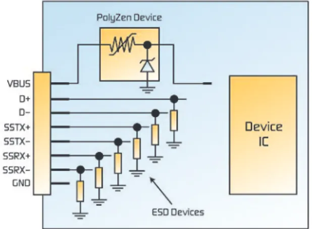
Figure 3 shows how installing a PolyZen device on the VBUS and six PESD devices on a typical USB circuit can help provide a coordinated overvoltage solution.
Figure 3. Coordinated device-side protection solution.
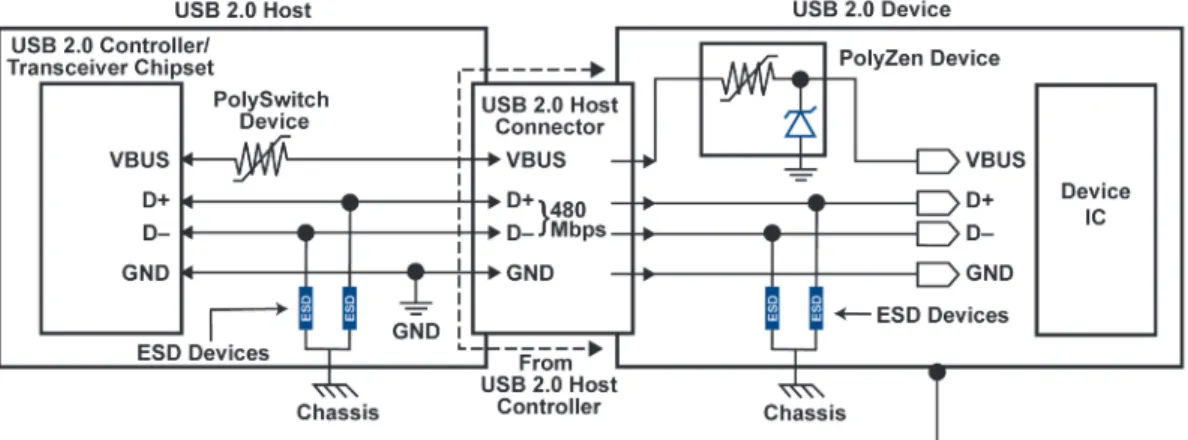
PolySwitch device on the VBUS port of a USB power source limits current in the event of a short circuit, prevents overcurrent damage caused by a sudden short circuit downstream, and helps achieve UL60950 compliance. Additionally, six TE PESD devices on the USB power source provide low-capacitance ESD protection in a small footprint package.
ESD Protection
Overvoltage transients are often the result of ESD and may occur on the power bus as well as the data lines. Although modern ICs are protected up to 2,000V, a human body can easily build up static charge that ranges up to 25,000V. In I/O port protection applications, a very-low-capacitance ESD device with fast clamping and recovery response is required on the data lines.
The existing USB 2.0 protocol allows for data transfer rates of up to 480Mbps and supports plug-and-play, hot-swappable installation and operation. In comparison, the USB 3.0 specification allows for data transfer rates of up to 5Gbps, with fall-back support for the lower-speed USB 2.0 specification.
USB 3.0 adds four new pins to the connector to support the new SuperSpeed interface: USB3_TX (differential pair) and USB3_RX (differential pair), as shown in Figure 4.
The SuperSpeed interface of USB 3.0 requires lower-capacitance ESD protection than that of USB 2.0. Adding very-low-capacitance PESD devices can help minimize insertion loss in order to meet eye diagram requirements of USB 3.0. With a typical capacitance of 0.2pF, and flat insertion loss to >6GHz, PESD devices are capable of supporting USB 3.0 application requirements and handling numerous ESD transients.
Compared to most traditional MLV (multilayer varistor) or TVS (transient voltage suppression) diode technologies, PESD devices provide lower capacitance, and their low-trigger and low-clamping voltage also helps protect sensitive electronic components. The devices are applicable for ESD protection on both USB 2.0’s high-speed D+ and D- signal lines and USB 3.0 SuperSpeed signal lines. Adding PESD devices to the circuit protection scheme yields protection levels that meet the specifications of IEC61000-4-2, which specifies 8kV (typ)/15kV (max) for contact mode and 15kV (typ)/25kV (max) for air discharge mode.
Figure 4. The new SuperSpeed interface lines (red) and the legacy USB interface lines (white).
Coordinated Circuit Protection
A coordinated protection scheme can be used to enhance protection against high-current, high-voltage and ESD transients in USB applications. Figures 5, 6, 7a and 7b
illustrate the circuit protection devices that are suitable for USB 2.0, USB 3.0 and Powered-B connector designs.
Figure 6. A coordinated circuit protection approach for USB 3.0.
Figure 7a - Bus-powered device with Powered-B plug (e.g., Standard Wireless Modem).
Figure 7b - Battery-powered device charged from DPWR pins and supplying power through VBUS.
Device Recommendations
PolySwitch overcurrent protection devices help designers meet the new high-current requirements of the USB 3.0 specification and provide a simple, space-saving current-limiting solution. PESD devices provide the low capacitance (typically 0.2pF) required for high-speed data transmission applications, and are available in the electronics industry's
most popular form factors. PolyZen devices offer designers the simplicity of a traditional clamping diode while obviating the need for significant heat sinking in the event of sustained overvoltage. This single device helps provide protection against damage caused by the use of improper power supplies, voltage transients, and other user-generated errors.
TE recommends the following devices for USB overcurrent protection.
TE recommends placing overvoltage protection devices on all USB-powered equipment, specifically on the VBUS port, as shown in the following table.
Recommended Parts
Ganged Ports per PolySwitch Device
USB Host Protocol Max allowed 1 2 3 4
current per port
USB 1.0 or 2.0 0.5A nanoSMDC075F miniSMDC160F miniSMDC200F miniSMDC260F USB 3.0 0.9A nanoSMDC150F miniSMDC260F N/A N/A
USB Charging
1.5A miniSMDC260F N/A N/A N/A
Enabled Port
USB VBUS Overvoltage Protection Recommendations
USB 2.0 USB 3.0 USB Charging Notes
PolyZen Device PolyZen Device PolyZen Device Lower Voltage ZEN056V130A24LS ZEN056V130A24LS ZEN056V230A16LS Clamping
PolyZen Device PolyZen Device PolyZen Device Lower Leakage ZEN065V130A24LS ZEN065V130A24LS ZEN065V230A16LS Current
TE recommends the following devices for ESD protection. Note: Increasing the number of ports raises the energy-absorbing-capacity requirement of the PolySwitch device.
miniSMD, nanoSMD, PolySwitch, PolyZen, TE Connectivity, TE connectivity (Logo) and TE (logo) are trademarks of the TE Connectivity Ltd. family of companies. Other logos, product and company names mentioned herein may be trademarks of their respective owners. All information, including illustrations, is believed to be accurate and reliable. However, users should independently evaluate the suitability of each product for their application. Tyco Electronics Corporation and/or its Affiliates in the TE Connectivity Ltd. family of companies (“TE”) makes no warranties as to the accuracy or completeness of the information, and disclaims any liability regarding its use. TE’s only obligations are those in the TE Standard Terms and Conditions of Sale and in no case will TE be liable for any incidental, indirect, or consequential damages arising from the sale, resale, use, or misuse of the product. Specifications are subject to change without notice. In addition, TE reserves the right to make changes without notification to Buyer — to materials or processing that do not affect compliance with any applicable specification.
©2011 Tyco Electronics Corporation, a TE Connectivity Ltd. company. All rights reserved. RCP0066E.0610 TE Circuit Protection
308 Constitution Drive
Menlo Park, CA USA 94025-1164 Tel : (800) 227-7040, (650) 361-6900 Fax : (650) 361-4600
www.circuitprotection.com
www.circuitprotection.com.hk (Chinese)