Available Online at www.ijpret.com 181
INTERNATIONAL JOURNAL OF PURE AND
APPLIED RESEARCH IN ENGINEERING AND
TECHNOLOGY
A PATH FOR HORIZING YOUR INNOVATIVE WORK
AN ENDURANCE-AWARE DISK-ON-BOARD SOLUTION FOR INDUSTRIAL
MEMORY
SHRUNKHALA NAIK, SONIA KUWELKAR, JAN GUNKE
Department of Electrical Engineering, G.H. Raisoni Institute of Engineering and Technology for Women, Nagpur
Accepted Date: 15/03/2016; Published Date: 01/05/2016
\
Abstract: The devices in network distribution systems are required to store and transfer
recorded information. These systems are equipped with a SD card to store the configuration
data, parameters and the device firmware. In price-sensitive applications, a low-cost way
rather than a flexible solution is more valuable to the market. The purpose of this project is
to study the possibilities of using a non-replaceable memory as a cost-efficient alternative to
the SD card and to implement the best solution.
Key Words: SD card, Flash, MRAM, FRAM, memory controller, PCB, DOB
Corresponding Author: SHRUNKHALA NAIK Access Online On:
www.ijpret.com
How to Cite This Article:
Available Online at www.ijpret.com 182 INTRODUCTION
Network distribution systems involve a telecontrol unit that is equipped with a SD card that serves the purpose of configuring the device and storing long-term information [1]. The portability of SD card also ensures a plug-and-play process. Thus the provision of a SD card adds functional flexibility to the device. However in some
cases, the market may require a low-cost alternative. Also these devices are susceptible to vibration and shock. Thus for mechanical reliability concerns, it is preferable to have an integrated solution instead of a remove-able card i.e. a disk-on-board or DOB solution. The industrial and commercial grade storage devices are mainly designed for systems which need a high level of reliability, stability and performance [3]. The industrial and commercial grade SD cards successfully meet these requirements but not at a low cost. Thus, there lies a tradeoff between the reliability and the cost of the device as illustrated below.
1. Master of Engineering, Microelectronics ETC Dept., Goa College of Engineering, Goa
University, Ponda, India, Mob. No. 07798631661 , [email protected]
2. Asst. Professor, ETC Dept., Goa College of Engineering, Goa University, Ponda, India.
3. Head of Architecture & Innovation Dept. R&D Siemens Ltd, Verna, India
Table 1: Types of flash used in applications
This project aims to build a memory device for cost sensitive applications, where the main focus lies in reducing the cost along with the best-effort maintenance of the present performance.
II. DEVICE DESIGN
Target application & SD card grade
Type of
NAND Flash used in the SD card
Bits/cell Susceptibility to data corruption (reliability)
Cost
Industrial SLC 1 Low High
Commercial MLC 2 Medium Medium
Consumer TLC and
higher
Available Online at www.ijpret.com 183 This section consists of three sub-sections. The first sub-section summarizes the study done in the process of selecting the components. The second sub-section discusses ways to interface memory to the host. The last sub-section includes the design details.
1. Component selection:
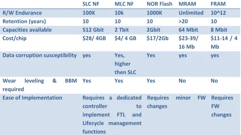
With the advancement of memory technologies, a number of new emerging memories [2] are being commercialized. The following table summarizes the comparison of five non-volatile memories with respect to their industrial requirements. These values are obtained from an electronic distributor called digikey [4]. The memory chips chosen for comparison are Micron 4GB SLC Flash, Micron 4GB MLC Flash, Micron 2Gbit NOR flash, Everspin 16Mb MRAM, Cypress 4Mb FRAM
SLC NF MLC NF NOR Flash MRAM FRAM
R/W Endurance 100K 10k 1000K Unlimited 10^12
Retention (years) 10 10 10 >20 10
Capacities available 512 Gbit 2 Tbit 2Gbit 64 Mbit 8 Mbit
Cost/chip $28/ 4GB $4/ 4 GB $17/2Gb $23-39/
16 Mb
$11-14 / 4 Mb
Data corruption susceptibility yes Yes,
higher then SLC
Yes yes yes
Wear leveling & BBM
required
Yes Yes Yes No No
Ease of Implementation Requires a dedicated
controller to
implement FTL and Lifecycle management functions
Requires minor FW changes
Requires FW changes
Table 2: Comparison of memories with respect to industrial requirements
The highlight of this study is the cost difference between the memories. It is clear that NAND Flash has the lowest cost for a given chip density. Moreover, it is only NAND Flash that is available in high densities ranging upto 2 Tbit. Thus NAND Flash memory is chosen for this work.
• The problem
Available Online at www.ijpret.com 184 disk-on-board solution. Hence incase of wear-out, the entire device will have to be replaced. Thus this solution will bring down the cost of the device but increase the overall costs in the long run due to frequent replacements. Hence the designed system must not only be cost efficient but also have greater lifetime.
• The solution
In order to enhance the device lifetime, the following measures are taken:
1) Select Flash with highest number of program-erase cycles
2) Implement appropriate lifecycle management mechanisms such as ECC,
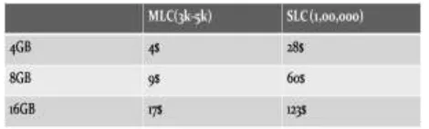
The following table shows a comparison between Micron MLC and SLC Flash for different densities.
Table 3: Cost comparison of SLC and MLC NAND Flash
It is seen that the number of program erase cycles is higher in case of SLC Flash. Hence, inspite of the higher cost, SLC flash is chosen to avoid frequent replacements and higher overall costs. Whenever an external memory device is connected to a system, for instance, a host PC, it expects to access a HDD (Hard disk drive). HDD’s are constructed of sectors, each of which is usually 512B or 4KB. On the other hand, flash devices are constructed of planes, blocks and pages. Therefore, translation of a sector access into a page or block access is required. This is done by a Flash translation layer i.e. FTL that maps the logical to physical addresses. FTL can be implemented on a memory controller or on the host as a part of firmware. [6].
Advanced error detection and correction algorithms can extend device endurance by correcting multiple read errors when they occur due to device aging. In order to implement a powerful ECC to correct multiple errors per sector, a controller has to be used with these functions in-built.
Available Online at www.ijpret.com 185 In many applications, data writes (translated into page programming cycles) occur less often than data reads (translated into page read cycles). Therefore there are data blocks on the devices which are more likely to be erased than others due to writes/updates from the host. If the average erase count across the entire chip or the entire device can be exploited by swapping blocks containing static data (i.e. data not often updated) with blocks containing data often updated, then overall endurance can be significantly increased. This procedure is termed “wear-leveling'. This further has two schemes: Static, Dynamic and Global. It has to be implemented by the controller.
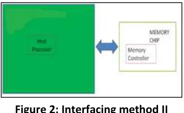
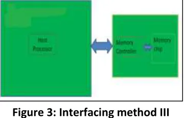
2. WAYS TO INTERFACE MEMORY TO THE HOST
Thus it is evident that, in order to interface flash memory to a device and ensure maximum possible device lifetime, a controller is required. The different ways in which a flash memory can be interfaced are:
1) Integrated on the host device such that the memory can be connected via a glueless
interface i.e. the target system has an internal memory controller.
Figure 1: Interfacing method I
2) Embedded in the memory device such that the host does not have to be involved in
implementing the controller functions.
Figure 2: Interfacing method II
3) As an external chip alongside the memory chip. This solution relieves the burden of the
Available Online at www.ijpret.com 186 Figure 3: Interfacing method III
This project implements the third solution in which an external controller is soldered in along with the memory chip for the following reasons:
• It does not burden the host processor with additional firmware changes to
accommodate the new memory.
• It is economical as compared to the expensive embedded controller-memory
alternative.
3. Design details:
This section includes an overview of the design and briefly describes the parts used in the prototype.
As mentioned in the previous section, a disk-on-board solution i.e. a memory system consisting of one or more flash chips connected to the host system via an intelligent memory controller is the chosen solution. For test purposes, a PCB prototype of this memory system will be made.
Figure 4: PCB Block diagram
Available Online at www.ijpret.com 187 signals, two ground and a power signal. This interface has a default frequency of 25 MHz and 50MHz in the high-speed mode. The flash interface has eight input-output lines and five control signals: write protect, write enable, output enable, ready/busy, command latch enable and address latch enable. It is a 128-pin TQFP package.
The memory ICs are two SLC 8Gbit Micron flash chips [8]. They are chosen from a wide range of options while considering the cost and its compatibility with the controller. Each IC is an industrial grade 48-pin package. Since the data inputs are not high speed (200 Bps), an asynchronous interface at about 40 MHz is adequate. The Flash IC is chosen with these factors in consideration.
The board runs on a voltage of 3.3 V. Proper care has been taken to meet the timing specifications of the interfaces to ensure correct operation.
III. CONCLUSION:
This work begins with a search for an appropriate non volatile memory. Once the SLC NAND flash memory is chosen, various ways of interfacing it to the target device are evaluated and a solution is chosen. The selection of alternatives at each step are made in an attempt to lower the cost and improve the lifetime of the system.
IV. FUTURE WORK:
The selected solution will be implemented as a PCB which will be tested for performance and endurance and the results will be compiled to show the pros and cons of this alternative.
V. REFERENCES
1. http://www.google.co.in/url?sa=t&rct=j&q=&esrc=s&frm=1&source=web&cd=3&cad=rja&u act=8&ved=0ahUKEwjbsOiRhfnKAhVJCY4KHa3tAIIQFggnMAI&url=http%3A%2F%2Fwww.sieme
ns.com%2Fdownload%3FDLA05_21376&usg=AFQjCNEGfrKljzu_Eaq0kcVi4kvwGRe-uA&bvm=bv.114195076,d.c2E
2. “Overview of emerging nonvolatile memory technologies” by Jagan Singh Meena, Simon
Min Sze, Umesh Chand and Tseung-Yuen Tseng- springer
3.
http://www.cactus-tech.com/files/cactus-tech.com/documents/whitepapers/Commercial%20and%20Industrial-Grade%20Products.pdf
4. http://www.digikey.com/product-search/en/integrated-circuits-ics/memory/2556980
5. Flash memory summit 2015
6. Inside Nand Flash memories by Rino Micheloni • Luca Crippa • Alessia Marelli [BOOK]
7. https://www.hyperstone.com/en/S8-SD-eMMC-Flash-Memory-Controller-265,399.html