Available Online at www.ijpret.com
382
INTERNATIONAL JOURNAL OF PURE AND
APPLIED RESEARCH IN ENGINEERING AND
TECHNOLOGY
A PATH FOR HORIZING YOUR INNOVATIVE WORK
TEST PATTERN GENERATOR FOR LOW POWER TESTING
AADHARSA VENUNADAN1, DR. AMEETA G. SINAI AMONKAR2 1. M.E.(Microelectronics), Goa College of Engineering, Ponda, Goa.
2. Head of Department, ETC Department, Goa College of Engineering, Ponda, Goa. Accepted Date: 27/02/2014 ; Published Date: 01/05/2014
p
\
Abstract:The need for low power testing is becoming increasingly important in today’s VLSI systems design. Extra power consumption can give rise to severe hazards in circuit reliability or provoke instant circuit damage. This paper discusses the implementation of a modified linear feedback shift register (LFSR) whose output sequence has less number of transitions between vectors. The technique uses bit swapping for vector ordering to achieve reduction in the overall switching activity in the circuit-under-test (CUT).
Keywords: Linear Feedback Shift Register, Bit Swapping, Switching Activity
Corresponding Author: AADHARSA VENUNADAN
Access Online On:
www.ijpret.com
How to Cite This Article:
Available Online at www.ijpret.com
383
INTRODUCTION
semiconductor manufacturing technology and the unprecedented levels of de-sign complexity and the gigahertz range of operating frequencies. These challenges include keeping the average and peak power dissipation and test application time within accept-able limits. Generally, power dissipation of a system in test mode is more than in normal mode. This is because a significant correlation exists between consecutive vectors applied during the circuit’s normal mode of operation, whereas this may not be necessarily true for applied test vectors in the test mode. Reduced correlation between the consecutive test vectors increases the switching activity and eventually the power dissipation in the circuit. The second reason of increasing the power dissipation during test is because the test engineers may test cores in parallel to reduce the test application time. This extra power (average or peak) can cause problems such as instantaneous power surge that causes circuit damage, difficulty in performance verification and decreased overall product yield and cost. Low power test application has become important in today’s VLSI design and test.
Several techniques have been developed to reduce the peak and average power dissipated during tests [8]. A direct technique to reduce power consumption is by running the test at a slower frequency than that in normal mode. This technique of reducing power consumption, while easy to implement, significantly increases the test application time. Furthermore, it fails in reducing peak-power consumption since it is independent of clock frequency.
The design of low-transition test-pattern generators (TPGs) is one of the most common and efficient techniques for low-power tests [4]–[6]. These algorithms modify the test vectors generated by the LFSR to get test vectors with a low number of transitions. The main drawback of these algorithms is that they aim only to reduce the average-power consumption while loading a new test vector, and they ignore the power consumption that results while scanning out the captured response or during the test cycle. Furthermore, some of these techniques may result in lower fault coverage and higher test application time.
Available Online at www.ijpret.com
384
Concepts Related To Testing Of Digital VLSI Circuits
Power dissipation in CMOS circuits In general, the power dissipation of complementary metal oxide semiconductors (CMOS) circuits can be divided into two main categories: static power and dynamic power.
Static power is the power dissipated by a gate when it is inactive, i.e. when it is not switching. A significant fraction of static power is caused by the reduced threshold voltage used in modern CMOS technology that prevents the gate from completely turning off, thus causing source to drain leakage. All the components of static power dissipation have a minor contribution to the total power dissipation, and can be minimised for well-designed circuits.
Dynamic power dissipation, which is the dominant source of power dissipation in CMOS circuits, occurs while the circuit is switching. The circuit is active when the applied voltage to an input of a cell changes, resulting in a logic transition in one or more of the outputs of the circuit at the transistor level. Hence, charging/discharging of the load capacitances of transistors is the main source of dynamic power dissipation.
Terms related to power consumption measures in testing
Energy: represents the total switching activity generated during the application of the complete test sequence.
Average Power: equals the total energy consumed during test divided by the test time in order to represent the average rate of energy consumption.
Instantaneous Power: corresponds to the power consumed at any given instant during testing.
Peak Power: corresponds to the highest value of instantaneous power measured during testing.
Weighted Switching Activity (WSA)
The weighted switching activity (WSA) of node i is the product “Si×Fi”, where, Si is the total
number of switching events at node i for the period T and Fi is the fan-out of node i. The total
Available Online at www.ijpret.com
385
Fault Coverage
A metric used to represent the percentage of faults detected using a fault model is the fault coverage (FC).The fault coverage can be represented as
FC=DC/TF (1)
where DF represents the number of detected faults, TF represents the total number of faults in the CUT.
Linear Feedback Shift Register As A TPG
Linear feedback shift registers (LFSRs) are extensively used for generating binary test sequences. This is because, with little overhead in the hardware area, a normal register can be configured to work as a test generator and, with an appropriate choice of the tap sequence (XOR locations), the LFSR can generate all possible output test vectors(except all-zero state).The tap sequence defines the feedback connections. LFSRs are characterized by their feedback connections represented as polynomials. For a nonzero initial state, the period of an LFSR is the number of states generated prior to repeating the initial state. An n-stage maximal length LFSR has a period of 2n -1 states and utilizes a primitive polynomial for its feedback connections. A maximal length LFSR can be enhanced with a nonlinear gate to produce an all-zero state. Pseudo exhaustive test pattern generators (TPGs) are usually based on maximal length LFSRs.
Furthermore, the pseudorandom behaviour of the LFSR reduces the correlation between successive test vectors, which means that it can achieve high fault coverage in a relatively short run of test vectors. However, this lack of correlation substantially increases the weighted switching activity (WSA) within the circuit-under-test (CUT). This often causes the power consumed during test mode operation to be much higher than during normal mode operation, which can lead to problems with battery lifetime and system reliability.
Available Online at www.ijpret.com
386
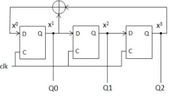
Fig 1: 3-stage external LFSR with characteristic polynomial p(x) = x3 +x+1
LFSRs can be divided into two main categories: external-XOR LFSR (simply external LFSR) and internal-XOR LFSR (simply internal LFSR). These are distinguished by the way in which XOR gates are inserted into the system. In an external LFSF the XORs appear only in the feedback, while in the internal LFSR the XORs appear between flip-flops.
Modified LFSR As A Low Transition TPG
The LFSR structure is modified in a way that it can re-order the outputs in a manner that reduces switching activity without compromising the fault coverage. This modified LFSR reduces the number of transitions in the CUT inputs by 25% using a bit-swapping technique [6]. The modified design can be implemented using a conventional LFSR and extra 2 x1 multiplexers. This design has the flexibility to be combined with other low-power techniques for further savings in power consumption.
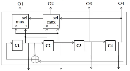
Architecture description
Available Online at www.ijpret.com
387 Fig. 2: Swapping arrangement for an LFSR [6]
The LFSR is modified by considering one of its outputs (say bit n) to be a selection line that will swap two neighbouring bits elsewhere in the LFSR when the selection line has a specific value (say 0). So if n is odd and bit n = 0, then bit 1 will be swapped with bit 2, bit 3 with bit 4, . . .,bit n-2 with bit n-1. If n is even and bit n = 0, then bit 1 will be swapped with bit 2, bit 3 with bit 4, . . . , bit n-3 with bit n-2. In all cases the selection line, bit n in this case, is excluded from the swapping operation. If bit n=1, then no swapping is performed.
Fig. 2 shows the bit swapping arrangement for an external LFSR. Here the output of the two cells will have its transition count reduced by Tsaved = 2(n−2) transitions. Since the two cells
originally produce 2 × 2n−1 transitions, then the resulting percentage saving is Tsaved% = 25%.
In the case where the selection cell is not directly linked to the cells being swapped through an XOR gate, each of the cells has the same share of savings (i.e., 25%).
In special cases where the cell that drives the selection line is linked to one of the swapped cells through an XOR gate, a single cell can save 50% transitions that were originally produced by an LFSR cell.
TABLE 1: SPECIAL CASES WHERE ONE CELL SAVES 50% OF THE TRANSITIONS [6]
LFSR Polynomial
LFSR Type Swapped cells Selection
line
MUX out 50% save
1st 2nd
xn+x+1 external C1 C2 Cn O2
xn+x+1 internal C1 Cn C2 O2
xn+xn-1+1 external Cn-1 Cn C1 O1
xn+xn-1+1 internal C1 Cn Cn-1 O1
xn+x2+1 external C1 C2 Cn O1
Available Online at www.ijpret.com
388
Important properties of the bit swapping LFSR
1) The bit swapping LFSR generates the same number of 1s and 0s at the output of multiplexers after swapping of two adjacent cells; hence, the probabilities of having a 0 or 1 at a certain cell of the scan chain before applying the test vectors are equal. Hence, the design retains an important feature of any random TPG.
2) The exhaustive set of generated test vectors will be the same as the test vectors generated by the corresponding unmodified LFSR, but their order will be different and the overall transitions in the primary inputs of CUT will be reduced by 25%.
RESULTS AND DISCUSSION
To observe the reduction in number of transitions in a cell of an LFSR various primitive polynomials were considered and the output sequence for an conventional LFSR and the LFSR modified using bit swapping technique were generated.
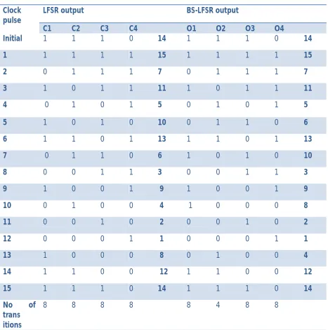
Fig. 3 shows the swapping arrangement for the LFSR with polynomial p(x) = x4+x+1, in which bits 1 and 2 of the LFSR are swapped when the selection line is driven by bit 4 of the LFSR.
Table 2 shows the obtained output sequence for the arrangement of fig. 2.
Fig. 3: 4-stage bit swapping LFSR with p(x) = x4+x+1
Available Online at www.ijpret.com
389
TABLE 2: OUTPUT SEQUENCE FOR THE ARRANGEMENT OF FIG. 3
Clock pulse
LFSR output BS-LFSR output
C1 C2 C3 C4 O1 O2 O3 O4
Initial 1 1 1 0 14 1 1 1 0 14
1 1 1 1 1 15 1 1 1 1 15
2 0 1 1 1 7 0 1 1 1 7
3 1 0 1 1 11 1 0 1 1 11
4 0 1 0 1 5 0 1 0 1 5
5 1 0 1 0 10 0 1 1 0 6
6 1 1 0 1 13 1 1 0 1 13
7 0 1 1 0 6 1 0 1 0 10
8 0 0 1 1 3 0 0 1 1 3
9 1 0 0 1 9 1 0 0 1 9
10 0 1 0 0 4 1 0 0 0 8
11 0 0 1 0 2 0 0 1 0 2
12 0 0 0 1 1 0 0 0 1 1
13 1 0 0 0 8 0 1 0 0 4
14 1 1 0 0 12 1 1 0 0 12
15 1 1 1 0 14 1 1 1 0 14
No of
trans itions
8 8 8 8 8 4 8 8
Available Online at www.ijpret.com
390
power consumed by the CUT during testing. A power analysis of the CUT when the generated test vectors are applied to the CUT can be done using a power analyser tool.
Since the vectors generated by the bit swapping technique are random, in some cases, it is possible that a higher fault coverage is obtained with lesser number of vectors applied to the CUT compared to the vectors generated by a LFSR. This inturn reduces the test application time.
Also, for a given primitive polynomial of the LFSR, WSA strongly depends on the seed selected[7]. The sensitivity of WSA on the primitive polynomial is much lower. Hence it is important to select the best seed for the LFSR to lower the WSA.
CONCLUSION
A TPG that generates test patterns that can reduce switching activity during test application is presented and simulated. The presented TPG is based on bit swapping technique. The results obtained
by the conventional LFSR are compared with those obtained by the bit swapping LFSR in terms of number of transitions. As theoretically determined, the observations of simulation show a 25% reduction in the number of transitions without any degradation in performance. The modified TPG can be used for low power testing, to generate test vectors for low power digital circuits.
Available Online at www.ijpret.com
391
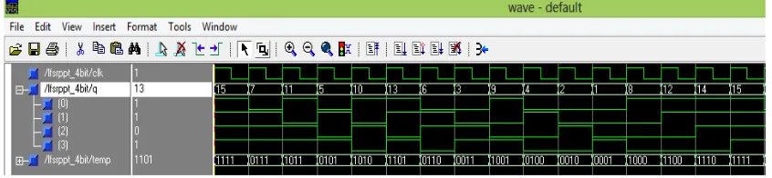
Fig. 5: Output sequence of bit swapping LFSR with polynomial x4+x+1
TABLE 3: TABLE SHOWING TOTAL NUMBER OF TRANSITIONS PRODUCED BY LFSR AND BS-LFSR
REFERENCE:
1. Niraj K. Jha, Sandeep Gupta, Testing of Digital Systems, Cambridge University Press, New York, 2003.
2. M. Bushnell and V. Agrawal, Essentials of Electronic Testing for Digital Memory,and Mixed Signal VLSI Circuits, Kluwer Academic Publishers, 2002.
3. V. Agrawal, C.R. Kime, and K. Saluja, "A tutorial on built-in self-test - part 1:principles", IEEE Design and Test of Computers, 10(1), March 1993.
4. S. Wang and S. Gupta, "DS-LFSR: A BIST TPG for low switching activity", IEEE Transactions on Computer-Aided Design of Integrated Circuits and Systems, 21(7), July 2002.
5. A.S. Abu-Issa and S.F. Quigley, "Bit-swapping LFSR and scan-chain ordering: A novel technique for peak - and average- power reduction in scan based BIST", IEEE Transactions on Computer-Aided Design of Integrated Circuits and Systems, 28(5), May 2009.
No. of stages of LFSR (n)
Polynomial Total no. of
transitions by LFSR
( n x 2(n-1))
Swapped cells
Total no.of
transitions by BS-LFSR
No. of
transitions reduced
3 x3+x+1 12 1 & 2 10 2
4 x4+x+1 32 1 & 2 28 4
5 x5+x2+1 80 1 & 2 72 8
Available Online at www.ijpret.com
392
6. P. Girard et al., “Low Energy BIST Design: Impact of the LFSR TPG Parameters on the Weighted Switching Activity,” Proc. Int’l Symp. on Circuits and Systems (ISCAS 99), IEEE CS Press, Los Alamitos, Calif., 1999.
7. P. Girard, “Survey of low-power testing of VLSI circuits”, IEEE Des. Test of Computers., vol. 19, no. 3, May/Jun. 2002.
![TABLE 1: SPECIAL CASES WHERE ONE CELL SAVES 50% OF THE TRANSITIONS [6]](https://thumb-us.123doks.com/thumbv2/123dok_us/8750027.1748306/6.595.66.535.550.691/table-special-cases-cell-saves-transitions.webp)