H. Zimmermann
Institute of Electrical Measurements and Circuit Design, Vienna University of Technology, Vienna, Austria
Abstract. An overview on integrated silicon photodiodes and photodiode integrated circuits (PDICs) or optoelectronic integrated circuits (OEICs) for optical storage systems (OSS) and fiber receivers is given. It is demonstrated, that by us-ing low-cost silicon technologies high-performance OEICs being true competitors for some III/V-semiconductor OE-ICs can be realized. OSS-OEOE-ICs with bandwidths of up to 380 MHz and fiber receivers with maximum data rates of up to 11 Gbps are described. Low-cost data comm receivers for plastic optical fibers (POF) as well as new circuit concepts for OEICs and highly parallel optical receivers are described also in the following.
1 Introduction
There is a wide field of applicatons for Opto ASICs. Inex-pensive optical receivers with top performance are in great demand. III-V semiconductors normally achieve the best pe-formance, while Si technologies offer low production costs. For long distance applications, with data rates of more than 40 Gbps, it is useful to accept high costs of III-V semicon-ductors to get the best performance. On the other hand these high costs make them unattractive for the mass markets of short distance applications where lower data rates are ade-quate, e.g. local-area networks, fiber to/in the home, optical interconnects on and between boards. Nevertheless it is nec-essary to use advanced circuit design to reach competitive re-sults with Si technologies. Si photodetectors can detect visi-ble and near-infrared light which is used for short distance communications, as well as for plastic-optical-fiber (POF) receivers and in optical pickup units for instance in DVD sys-tems.
Optoelectronic integrated circuits (OEICs) are used for very compact designs and low-cost applications. They
com-Correspondence to: H. Zimmermann
2 H. Zimmermann: High-End Silicon PDICs
Fig. 1. PIN photodiode integration in standard buried collector (SBC) bipolar technology [Yamamoto (1995)]
Fig. 2. Schematic of a 2.5Gbps silicon receiver OEIC with large-diameter photodiode [Swoboda (2004)]
tivity of –17.2dBm compared to –15.7dBm of a GaAs OEIC [Lang (2001)], whereby the die area of the Si OEIC was one fifth of that of the GaAs OEIC and the power consumption was one third.
3 Two-stage OEIC for the use in DVD
In [Leeb (2004)] an amplifier architecture that uses a differ-ential transimpedance amplifier in the first stage and an op-erational amplifier in a second stage is presented.
The used amplifier structure is shown in Fig. 4. The main I/V converter and the dummy I/V converter are connected by a current sourceI0and therefore both of them contribute gain to the input stage. The second stage is designed as sub-tractor amplifier and subtracts and amplifies the differential output voltage of the first–stage amplifiers. Furthermore a reference voltageVref is added to reach a single-ended
out-Fig. 3. Microphotograph of a 2.5Gbps silicon receiver OEIC with large-diameter photodiode [Swoboda (2004)]
put with low offset voltage compared toVref. This architec-ture together with the capacitanceCCOMPenables a doubled transimpedance with the same value of the feedback resis-torRfb compared to other concepts. This leads to a dou-bled differential transimpedance compared to the architec-ture used in [Kieschnick (1999), Zimmermann (2000), and Kieschnick (2003)] for the sameRfbvalue. The bandwidth was increased by a factor of 6.8 compared to a two-stage amplifier presented in [Takimoto (1998)] and by a factor of 2.6 compared to [Kieschnick (1999)]. In addition, the photo-sensitivity was increased by a factor of about 10 compared to [Kieschnick (1999), Zimmermann (2000)]. In total, the transimpedance–bandwidth product was increased by a fac-tor of 26 compared to [Kieschnick (1999)].
The analog modulation port of the network analyzer was used to modulate the laser source for the measurement of the frequnency response. In Fig. 5 the measured frequency response is depicted. It can be seen that the upper -3dB cut-off frequency of the two-stage transimpedance amplifier is 380MHz. The lower cut-off frequency is 450kHz, for fre-quencies below that lower cut-off frequency the gain drops by 6dB.
4 130MHz-bandwidth, 120dB-dynamic-range tran-simpedance amplifier (TIA) in0.35µmSiGe BiCMOS
The basic circuit topology of the 130MHz-bandwidth, 120dB-dynamic-range TIA in0.35µmSiGe BiCMOS
[Mi-Fig. 1. PIN photodiode integration in standard buried collec-tor (SBC) bipolar technology (Yamamoto, 1995).
bine the photodetector and the receiver circuit on a single chip and therefore mounting and handling are much cheaper and the area consumption and weight is far below a multi-chip solution. In the next years there will be a demand for high volumes of low-cost highly reliable OEICs for opti-cal buses in cars and in optiopti-cal storage systems, e.g. CD-ROM, DVD, Digital Video Recording and Enhanced Video Disk (EVD). For high performance OEICs, pin photodiodes are integrated in Si processes.
2 Large–diameter integrated–photodiode OEIC
A vertical PIN photodiode was integrated in a 0.6µm BiC-MOS process. It is similar in design to the diode presented in (Yamamoto, 1995) which cross section is depicted in Fig. 1. Deep N plugs after low-doped N-epitaxial steps form the connection from the Si surface to the N+ buried–layer cath-ode. The electrical isolation between the npn transistors and the N-wells is formed by a P-isolation layer, which separates them. (Yamamoto, 1995) presented a bandwidth of 300 MHz at 780 nm light with a reverse bias voltage of 3 V. However, the reverse bias voltage can be larger than the chip supply
84Fig. 1. PIN photodiode integration in standard buried collector H. Zimmermann: High-End Silicon PDICs (SBC) bipolar technology [Yamamoto (1995)]
Fig. 2. Schematic of a 2.5Gbps silicon receiver OEIC with large-diameter photodiode [Swoboda (2004)]
tivity of –17.2dBm compared to –15.7dBm of a GaAs OEIC [Lang (2001)], whereby the die area of the Si OEIC was one fifth of that of the GaAs OEIC and the power consumption was one third.
3 Two-stage OEIC for the use in DVD
In [Leeb (2004)] an amplifier architecture that uses a differ-ential transimpedance amplifier in the first stage and an op-erational amplifier in a second stage is presented.
The used amplifier structure is shown in Fig. 4. The main I/V converter and the dummy I/V converter are connected by a current sourceI0and therefore both of them contribute gain to the input stage. The second stage is designed as sub-tractor amplifier and subtracts and amplifies the differential output voltage of the first–stage amplifiers. Furthermore a reference voltageVref is added to reach a single-ended
out-Fig. 3. Microphotograph of a 2.5Gbps silicon receiver OEIC with large-diameter photodiode [Swoboda (2004)]
put with low offset voltage compared toVref. This architec-ture together with the capacitanceCCOMPenables a doubled transimpedance with the same value of the feedback resis-torRfbcompared to other concepts. This leads to a dou-bled differential transimpedance compared to the architec-ture used in [Kieschnick (1999), Zimmermann (2000), and Kieschnick (2003)] for the sameRfbvalue. The bandwidth was increased by a factor of 6.8 compared to a two-stage amplifier presented in [Takimoto (1998)] and by a factor of 2.6 compared to [Kieschnick (1999)]. In addition, the photo-sensitivity was increased by a factor of about 10 compared to [Kieschnick (1999), Zimmermann (2000)]. In total, the transimpedance–bandwidth product was increased by a fac-tor of 26 compared to [Kieschnick (1999)].
The analog modulation port of the network analyzer was used to modulate the laser source for the measurement of the frequnency response. In Fig. 5 the measured frequency response is depicted. It can be seen that the upper -3dB cut-off frequency of the two-stage transimpedance amplifier is 380MHz. The lower cut-off frequency is 450kHz, for fre-quencies below that lower cut-off frequency the gain drops by 6dB.
4 130MHz-bandwidth, 120dB-dynamic-range tran-simpedance amplifier (TIA) in0.35µmSiGe BiCMOS
The basic circuit topology of the 130MHz-bandwidth, 120dB-dynamic-range TIA in0.35µmSiGe BiCMOS
[Mi-Fig. 2. Schematic of a 2.5 Gbps silicon receiver OEIC with large-diameter photodiode (Swoboda, 2004).
2 H. Zimmermann: High-End Silicon PDICs
Fig. 1. PIN photodiode integration in standard buried collector (SBC) bipolar technology [Yamamoto (1995)]
Fig. 2. Schematic of a 2.5Gbps silicon receiver OEIC with large-diameter photodiode [Swoboda (2004)]
tivity of –17.2dBm compared to –15.7dBm of a GaAs OEIC [Lang (2001)], whereby the die area of the Si OEIC was one fifth of that of the GaAs OEIC and the power consumption was one third.
3 Two-stage OEIC for the use in DVD
In [Leeb (2004)] an amplifier architecture that uses a differ-ential transimpedance amplifier in the first stage and an op-erational amplifier in a second stage is presented.
The used amplifier structure is shown in Fig. 4. The main I/V converter and the dummy I/V converter are connected by a current sourceI0and therefore both of them contribute gain to the input stage. The second stage is designed as sub-tractor amplifier and subtracts and amplifies the differential output voltage of the first–stage amplifiers. Furthermore a reference voltageVrefis added to reach a single-ended
out-Fig. 3. Microphotograph of a 2.5Gbps silicon receiver OEIC with large-diameter photodiode [Swoboda (2004)]
put with low offset voltage compared toVref. This architec-ture together with the capacitanceCCOMPenables a doubled transimpedance with the same value of the feedback resis-torRfbcompared to other concepts. This leads to a dou-bled differential transimpedance compared to the architec-ture used in [Kieschnick (1999), Zimmermann (2000), and Kieschnick (2003)] for the sameRfbvalue. The bandwidth was increased by a factor of 6.8 compared to a two-stage amplifier presented in [Takimoto (1998)] and by a factor of 2.6 compared to [Kieschnick (1999)]. In addition, the photo-sensitivity was increased by a factor of about 10 compared to [Kieschnick (1999), Zimmermann (2000)]. In total, the transimpedance–bandwidth product was increased by a fac-tor of 26 compared to [Kieschnick (1999)].
The analog modulation port of the network analyzer was used to modulate the laser source for the measurement of the frequnency response. In Fig. 5 the measured frequency response is depicted. It can be seen that the upper -3dB cut-off frequency of the two-stage transimpedance amplifier is 380MHz. The lower cut-off frequency is 450kHz, for fre-quencies below that lower cut-off frequency the gain drops by 6dB.
4 130MHz-bandwidth, 120dB-dynamic-range tran-simpedance amplifier (TIA) in0.35µmSiGe BiCMOS
The basic circuit topology of the 130MHz-bandwidth, 120dB-dynamic-range TIA in0.35µmSiGe BiCMOS
[Mi-Fig. 3. Microphotograph of a 2.5 Gbps silicon receiver OEIC with large-diameter photodiode (Swoboda, 2004).
voltage of 5 V due to the fact that the N cathode is realized in a P-type substrate. This is important to speed up the carrier drift and to increase the bandwidth.
Run with a bias voltage of 12 V, a bandwith of more than 1.35 GHz was reached with a 660 nm laser diode (Swoboda, 2004). The simplified schematic of this 2.5 Gbps Si receiver OEIC with large-diameter photodiode is depicted in Fig. 2. A resopsivity of 0.36 A/W was achieved due to the thick in-trinsic layer. In Fig. 3, a microphotograph of the OEIC re-ceiver is depicted. The large photodiode with a diameter of 300µm can be clearly seen. The chip dimensions are 890µm times 870µm. The Si OEIC achieved a sensitiv-ity of−17.2 dBm compared to−15.7 dBm of a GaAs OEIC (Lang, 2001), whereby the die area of the Si OEIC was one fifth of that of the GaAs OEIC and the power consumption was one third.
H. Zimmermann: High-End Silicon PDICs 3
Fig. 4. Schematic of a 380MHz two-stage OEIC for the use in DVD [Leeb (2004)]
Fig. 5. Frequency response of a 380MHz two-stage OEIC for the use in DVD [Leeb (2004)]
cusik (2007)] with implemented compression is shown in Fig. 6.
The circuit consists of three transistor stages: the first in common–collector configuration (Q0) followed by a common–emitter voltage amplifier (Q1) and as third stage a common–collector voltage buffer (Q2). The feedback resis-torRf = 22kΩis connected from the output of the third
Fig. 6. Schematic of a 130MHz-bandwidth, 120dB-dynamic-range TIA in0.35µmSiGe BiCMOS [Micusik (2007)]
stage to the input of the first transistor stage. For mini-mum electronic noise the input common–collector stage (Q0) can be biased without any influence of the following stages. There are two types of operation. In the linear region the transistors Q5 and Q6 are off and therefore do not affect the circuit for small input currents. In the compression region the transistor Q6 is on and provides current to the input and therefore a parallel path toRfwhich leads to a lower overall transimpedance of the TIA. Stability over the full input cur-rent range is provided by the compensation circuit consisting of Q3, Q4 and Q5. The open-loop gain of the circuit is low-ered by the compensation circuit dynamically and therefore the phase margin of the loop gain is kept large enough. In the linear region the TIA itself is the limiting element regarding to the bandwidth (BW). In the compensation region the BW of the TIA increases and the limiting elements are the follow-ing stages, e.g. the differential50Ωdriver. The full width at half maximum (FWHM) of the input current pulses used for characterization was 10ns with a rise and fall time of 1.5ns. The circuit proposed in [Micusik (2007)] exhibits the highest dynamic range (120 dB) for the input current compared to the literature. The power consumption of the TIA alone is 2mA from a 5V power supply. The complete receiver circuit in-cluding a50Ω, 1.7V peak-to-peak differential output driver consumes an area of1.24mm2in0.35µmSiGe BiCMOS technology and the complete power consumption is 390mW. A microphotograph of the 130MHz-bandwidth, 120dB-dynamic-range TIA in0.35µmSiGe BiCMOS is depicted in Fig. 7.
5 11Gbps optical receiver
[Swoboda (2006)] presented a monolithically integrated sil-icon optical receiver for 850nm light. The used photodi-Fig. 4. Schematic of a 380 MHz two-stage OEIC for the use in DVD
(Leeb, 2004).
H. Zimmermann: High-End Silicon PDICs 3
Fig. 4. Schematic of a 380MHz two-stage OEIC for the use in DVD [Leeb (2004)]
Fig. 5. Frequency response of a 380MHz two-stage OEIC for the use in DVD [Leeb (2004)]
cusik (2007)] with implemented compression is shown in Fig. 6.
The circuit consists of three transistor stages: the first in common–collector configuration (Q0) followed by a common–emitter voltage amplifier (Q1) and as third stage a common–collector voltage buffer (Q2). The feedback resis-torRf = 22kΩis connected from the output of the third
Fig. 6. Schematic of a 130MHz-bandwidth, 120dB-dynamic-range TIA in0.35µmSiGe BiCMOS [Micusik (2007)]
stage to the input of the first transistor stage. For mini-mum electronic noise the input common–collector stage (Q0) can be biased without any influence of the following stages. There are two types of operation. In the linear region the transistors Q5 and Q6 are off and therefore do not affect the circuit for small input currents. In the compression region the transistor Q6 is on and provides current to the input and therefore a parallel path toRfwhich leads to a lower overall transimpedance of the TIA. Stability over the full input cur-rent range is provided by the compensation circuit consisting of Q3, Q4 and Q5. The open-loop gain of the circuit is low-ered by the compensation circuit dynamically and therefore the phase margin of the loop gain is kept large enough. In the linear region the TIA itself is the limiting element regarding to the bandwidth (BW). In the compensation region the BW of the TIA increases and the limiting elements are the follow-ing stages, e.g. the differential50Ωdriver. The full width at half maximum (FWHM) of the input current pulses used for characterization was 10ns with a rise and fall time of 1.5ns. The circuit proposed in [Micusik (2007)] exhibits the highest dynamic range (120 dB) for the input current compared to the literature. The power consumption of the TIA alone is 2mA from a 5V power supply. The complete receiver circuit in-cluding a50Ω, 1.7V peak-to-peak differential output driver consumes an area of1.24mm2in0.35µmSiGe BiCMOS
technology and the complete power consumption is 390mW. A microphotograph of the 130MHz-bandwidth, 120dB-dynamic-range TIA in0.35µmSiGe BiCMOS is depicted in Fig. 7.
5 11Gbps optical receiver
[Swoboda (2006)] presented a monolithically integrated sil-icon optical receiver for 850nm light. The used
photodi-Fig. 5. Frequency response of a 380 MHz two-stage OEIC for the use in DVD (Leeb, 2004).
3 Two-stage OEIC for the use in DVD
In (Leeb, 2004) an amplifier architecture that uses a differen-tial transimpedance amplifier in the first stage and an opera-tional amplifier in a second stage is presented.
The used amplifier structure is shown in Fig. 4. The main I/V converter and the dummy I/V converter are connected by a current source (I0) and therefore both of them contribute
gain to the input stage. The second stage is designed as subtractor amplifier and subtracts and amplifies the differen-tial output voltage of the first–stage amplifiers. Furthermore a reference voltage (Vref) is added to reach a single-ended
output with low offset voltage compared to (Vref). This
ar-chitecture together with the capacitance (CCOMP) enables a
doubled transimpedance with the same value of the feed-back resistor (Rf b) compared to other concepts. This leads to a doubled differential transimpedance compared to the
Fig. 7. Micorphotograph of a 130MHz-bandwidth, 120dB-dynamic-range TIA in0.35µmSiGe BiCMOS [Micusik (2007)]
ode has a diameter of50µmand therefore matches exactly a50µmmultimode fiber.
The schematic of the input circuit including a simplified schematic of the following stages is depicted in Fig. 8. A TIA consisting of T1, T3, R1, R3, R5, C1, C3, and Rfb1 is used to convert the photo current into an output voltage. The transimpedance is500Ω. The output voltage of the TIA subtracted by a reference voltage is amplified frequency de-pendent. The gain has the inverse characteristic to the pho-todiode frequency response. This is realized by a cascode difference amplifier consisting of T5, T6, T7, T8, R7 and R8 including frequency-dependent coupling elements. Rd and Cd compensate the photodiode drift time and the small diffu-sion part is compensated with C1, Rl1 and Rl2. A nearly flat frequency response with a linear phase is reached with this equalizer. TIA and equalizer are followed by three limiting amplifiers to improve the gain and drive a differential 100Ω load. The average photo currentIAV Ggenerated by a dif-ferential integrator, a controlling circuit and a dummy TIA is provided to the dummy TIA via Rc. Therefore symmetrical clipping of the 0s and 1s is provided in case of optical over-drive. The background light is suppressed by a lower cut-off frequency of 30kHz introduced by the controlling circuit.
The bit–error rate (BER) was measured with a bit error an-alyzer for different data rates, optical power levels, and two different lengths of the pseudo random bit sequence (PRBS). The summarized results are depicted in Fig. 9. An eye dia-gram at 11Gbps and a PRBS of231−1at minimum optical power of -8.9dBm for a BER of10−9is shown in the same figure.
Fig. 8. Simplified schematic of 11Gbps optical receiver [Swoboda (2006)]
Fig. 9. Bit error rate vs. average optical power of 11Gbps optical receiver [Swoboda (2006)]
6 TIA with CCVD feedback
In conventional TIA topologies in integrated circuits the high-ohmic feedback resistor can be the bandwidth limiting element due to parasitic capacitances to the substrate. To avoid this, a new concept was presented in [Seidl (2004)]. It introduces a capacitive-coupled voltage divider (CCVD) in-stead of an ohmic resistor in the feedback path of the TIA, like depicted in Fig. 10. With this new topology the band-width was raised from 67MHz to 387MHz. Both topologies were realized for better comparison.
The CCVD TIA offers the opportunity to realize higher bandwidth-transimpedance products in one amplifier stage than others known from the literature did in 2- or 3-stage TIAs [Hehemann (2002)]. This results in less chip area, less power consumption and less offset of TIAs.
Fig. 6. Schematic of a 130 MHz-bandwidth, 120 dB-dynamic-range TIA in 0.35µm SiGe BiCMOS (Micusik, 2007).
4 H. Zimmermann: High-End Silicon PDICs
Fig. 7. Micorphotograph of a 130MHz-bandwidth, 120dB-dynamic-range TIA in0.35µmSiGe BiCMOS [Micusik (2007)]
ode has a diameter of50µmand therefore matches exactly a50µmmultimode fiber.
The schematic of the input circuit including a simplified schematic of the following stages is depicted in Fig. 8. A TIA consisting of T1, T3, R1, R3, R5, C1, C3, and Rfb1 is used to convert the photo current into an output voltage. The transimpedance is500Ω. The output voltage of the TIA subtracted by a reference voltage is amplified frequency de-pendent. The gain has the inverse characteristic to the pho-todiode frequency response. This is realized by a cascode difference amplifier consisting of T5, T6, T7, T8, R7 and R8 including frequency-dependent coupling elements. Rd and Cd compensate the photodiode drift time and the small diffu-sion part is compensated with C1, Rl1 and Rl2. A nearly flat frequency response with a linear phase is reached with this equalizer. TIA and equalizer are followed by three limiting amplifiers to improve the gain and drive a differential 100Ω load. The average photo currentIAV Ggenerated by a dif-ferential integrator, a controlling circuit and a dummy TIA is provided to the dummy TIA via Rc. Therefore symmetrical clipping of the 0s and 1s is provided in case of optical over-drive. The background light is suppressed by a lower cut-off frequency of 30kHz introduced by the controlling circuit.
The bit–error rate (BER) was measured with a bit error an-alyzer for different data rates, optical power levels, and two different lengths of the pseudo random bit sequence (PRBS). The summarized results are depicted in Fig. 9. An eye dia-gram at 11Gbps and a PRBS of231−1at minimum optical power of -8.9dBm for a BER of10−9is shown in the same figure.
Fig. 8. Simplified schematic of 11Gbps optical receiver [Swoboda (2006)]
Fig. 9. Bit error rate vs. average optical power of 11Gbps optical receiver [Swoboda (2006)]
6 TIA with CCVD feedback
In conventional TIA topologies in integrated circuits the high-ohmic feedback resistor can be the bandwidth limiting element due to parasitic capacitances to the substrate. To avoid this, a new concept was presented in [Seidl (2004)]. It introduces a capacitive-coupled voltage divider (CCVD) in-stead of an ohmic resistor in the feedback path of the TIA, like depicted in Fig. 10. With this new topology the band-width was raised from 67MHz to 387MHz. Both topologies were realized for better comparison.
The CCVD TIA offers the opportunity to realize higher bandwidth-transimpedance products in one amplifier stage than others known from the literature did in 2- or 3-stage TIAs [Hehemann (2002)]. This results in less chip area, less power consumption and less offset of TIAs.
Fig. 7. Micorphotograph of a 130 MHz-bandwidth, 120 dB-dynamic-range TIA in 0.35µm SiGe BiCMOS (Micusik, 2007).
chitecture used in (Kieschnick, 1999, Zimmermann, 2000, and Kieschnick, 2003) for the same (Rf b) value. The band-width was increased by a factor of 6.8 compared to a two-stage amplifier presented in (Takimoto, 1998) and by a fac-tor of 2.6 compared to (Kieschnick, 1999). In addition, the photo-sensitivity was increased by a factor of about 10 com-pared to (Kieschnick, 1999, Zimmermann, 2000). In total, the transimpedance–bandwidth product was increased by a factor of 26 compared to (Kieschnick, 1999).
The analog modulation port of the network analyzer was used to modulate the laser source for the measurement of the frequnency response. In Fig. 5 the measured frequency response is depicted. It can be seen that the upper−3 dB cut-off frequency of the two-stage transimpedance amplifier is 380 MHz. The lower cut-off frequency is 450 kHz, for fre-quencies below that lower cut-off frequency the gain drops by 6 dB.
Fig. 7. Micorphotograph of a 130MHz-bandwidth, 120dB-dynamic-range TIA in0.35µmSiGe BiCMOS [Micusik (2007)]
ode has a diameter of50µmand therefore matches exactly a50µmmultimode fiber.
The schematic of the input circuit including a simplified schematic of the following stages is depicted in Fig. 8. A TIA consisting of T1, T3, R1, R3, R5, C1, C3, and Rfb1 is used to convert the photo current into an output voltage. The transimpedance is500Ω. The output voltage of the TIA subtracted by a reference voltage is amplified frequency de-pendent. The gain has the inverse characteristic to the pho-todiode frequency response. This is realized by a cascode difference amplifier consisting of T5, T6, T7, T8, R7 and R8 including frequency-dependent coupling elements. Rd and Cd compensate the photodiode drift time and the small diffu-sion part is compensated with C1, Rl1 and Rl2. A nearly flat frequency response with a linear phase is reached with this equalizer. TIA and equalizer are followed by three limiting amplifiers to improve the gain and drive a differential 100Ω load. The average photo currentIAV G generated by a dif-ferential integrator, a controlling circuit and a dummy TIA is provided to the dummy TIA via Rc. Therefore symmetrical clipping of the 0s and 1s is provided in case of optical over-drive. The background light is suppressed by a lower cut-off frequency of 30kHz introduced by the controlling circuit.
The bit–error rate (BER) was measured with a bit error an-alyzer for different data rates, optical power levels, and two different lengths of the pseudo random bit sequence (PRBS). The summarized results are depicted in Fig. 9. An eye dia-gram at 11Gbps and a PRBS of231−1at minimum optical power of -8.9dBm for a BER of10−9is shown in the same figure.
Fig. 8. Simplified schematic of 11Gbps optical receiver [Swoboda (2006)]
Fig. 9. Bit error rate vs. average optical power of 11Gbps optical receiver [Swoboda (2006)]
6 TIA with CCVD feedback
In conventional TIA topologies in integrated circuits the high-ohmic feedback resistor can be the bandwidth limiting element due to parasitic capacitances to the substrate. To avoid this, a new concept was presented in [Seidl (2004)]. It introduces a capacitive-coupled voltage divider (CCVD) in-stead of an ohmic resistor in the feedback path of the TIA, like depicted in Fig. 10. With this new topology the band-width was raised from 67MHz to 387MHz. Both topologies were realized for better comparison.
The CCVD TIA offers the opportunity to realize higher bandwidth-transimpedance products in one amplifier stage than others known from the literature did in 2- or 3-stage TIAs [Hehemann (2002)]. This results in less chip area, less power consumption and less offset of TIAs.
Fig. 8. Simplified schematic of a 11 Gbps optical receiver (Swo-boda, 2006).
4 130 MHz-bandwidth, 120 dB-dynamic-range tran-simpedance amplifier (TIA) in 0.35µm SiGe BiC-MOS
The basic circuit topology of the 130 MHz-bandwidth, 120 dB-dynamic-range TIA in 0.35µm SiGe BiCMOS (Mi-cusik, 2007) with implemented compression is shown in Fig. 6.
The circuit consists of three transistor stages: the first in common–collector configuration (Q0) followed by a common–emitter voltage amplifier (Q1) and as third stage a common–collector voltage buffer (Q2). The feedback re-sistor (Rf=22 k) is connected from the output of the third stage to the input of the first transistor stage. For mini-mum electronic noise the input common–collector stage (Q0) can be biased without any influence of the following stages. There are two types of operation. In the linear region the transistors Q5 and Q6 are off and therefore do not affect the circuit for small input currents. In the compression region the transistor Q6 is on and provides current to the input and therefore a parallel path to (Rf) which leads to a lower over-all transimpedance of the TIA. Stability over the full input current range is provided by the compensation circuit con-sisting of Q3, Q4 and Q5. The open-loop gain of the circuit is lowered by the compensation circuit dynamically and there-fore the phase margin of the loop gain is kept large enough. In the linear region the TIA itself is the limiting element re-garding to the bandwidth (BW). In the compensation region the BW of the TIA increases and the limiting elements are the following stages, e.g. the differential 50driver. The full width at half maximum (FWHM) of the input current pulses used for characterization was 10 ns with a rise and fall time of 1.5 ns. The circuit proposed in (Micusik, 2007) ex-hibits the highest dynamic range (120 dB) for the input cur-rent compared to the literature. The power consumption of
86 H. Zimmermann: High-End Silicon PDICs
Fig. 7.
Micorphotograph of a 130MHz-bandwidth,
120dB-dynamic-range TIA in
0.35µm
SiGe BiCMOS [Micusik (2007)]
ode has a diameter of
50
µm
and therefore matches exactly
a
50
µm
multimode fiber.
The schematic of the input circuit including a simplified
schematic of the following stages is depicted in Fig. 8. A
TIA consisting of T1, T3, R1, R3, R5, C1, C3, and Rfb1
is used to convert the photo current into an output voltage.
The transimpedance is
500Ω
. The output voltage of the TIA
subtracted by a reference voltage is amplified frequency
de-pendent. The gain has the inverse characteristic to the
pho-todiode frequency response. This is realized by a cascode
difference amplifier consisting of T5, T6, T7, T8, R7 and R8
including frequency-dependent coupling elements. Rd and
Cd compensate the photodiode drift time and the small
diffu-sion part is compensated with C1, Rl1 and Rl2. A nearly flat
frequency response with a linear phase is reached with this
equalizer. TIA and equalizer are followed by three limiting
amplifiers to improve the gain and drive a differential 100
Ω
load. The average photo current
I
AV Ggenerated by a
dif-ferential integrator, a controlling circuit and a dummy TIA is
provided to the dummy TIA via Rc. Therefore symmetrical
clipping of the 0s and 1s is provided in case of optical
over-drive. The background light is suppressed by a lower cut-off
frequency of 30kHz introduced by the controlling circuit.
The bit–error rate (BER) was measured with a bit error
an-alyzer for different data rates, optical power levels, and two
different lengths of the pseudo random bit sequence (PRBS).
The summarized results are depicted in Fig. 9. An eye
dia-gram at 11Gbps and a PRBS of
2
31−
1
at minimum optical
power of -8.9dBm for a BER of
10
−9is shown in the same
figure.
Fig. 8. Simplified schematic of 11Gbps optical receiver [Swoboda
(2006)]
Fig. 9. Bit error rate vs. average optical power of 11Gbps optical
receiver [Swoboda (2006)]
6
TIA with CCVD feedback
In conventional TIA topologies in integrated circuits the
high-ohmic feedback resistor can be the bandwidth limiting
element due to parasitic capacitances to the substrate. To
avoid this, a new concept was presented in [Seidl (2004)]. It
introduces a capacitive-coupled voltage divider (CCVD)
in-stead of an ohmic resistor in the feedback path of the TIA,
like depicted in Fig. 10. With this new topology the
band-width was raised from 67MHz to 387MHz. Both topologies
were realized for better comparison.
The CCVD TIA offers the opportunity to realize higher
bandwidth-transimpedance products in one amplifier stage
than others known from the literature did in 2- or 3-stage
TIAs [Hehemann (2002)]. This results in less chip area, less
power consumption and less offset of TIAs.
Fig. 9. Bit error rate vs. average optical power of a 11 Gbps optical receiver (Swoboda, 2006).
H. Zimmermann: High-End Silicon PDICs 5
Fig. 10. Schematic of 1-stage transimpedance amplifier with CCVD [Seidl (2004)]
Fig. 11. Highly parallel optical receiver [Swoboda et al (2006)]
7 Highly parallel optical receiver OEIC
In [Swoboda et al (2006)] a highly parallel optical receiver OEIC in a0.6µmSi BiCMOS technology was presented. It contains 36 channels with integrated PIN photodiode and a data rate of 3Gbps each. This very compact design with a pitch of250µmrequires a special layout of the receiver to minimize crosstalk. The measured sensitivity at 3Gbps is –17dBm at 850nm in each channel. This means that the presented receiver OEIC offers an over–all data rate of more than 100Gbps combined with a matching laser array on the sender side. Figure 11 shows a microphotograph of a test chip for the receiver chip.
The power consumption of the OEIC is 809mW including that of a laser driver for a return channel and a loss-of-power
Fig. 12. Block diagram of optical distance measurement / 3D cam-era with continuous wave system
detector. The crosstalk between the channels is below -40dB.
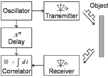
8 Optical distance measurement
Sensors for capturing 3D information of a scene in real time i.e. in a few milliseconds are still not available on the low-cost market on a grand scale. Mass products, for example neighbour-lane supervision or passenger recognition airbag control in a modern car, can use them. The interesting dis-tance range for these sensors is form cm up to some meters. It is important for robust low-cost sensors to avoid moving mechanical parts. The integrated optical distance measure-ment sensors presented here work on the principle of time-of-flight. It is based on the measurement of runtime of mod-ulated light from a laser source to the surface of a diffuse reflecting object and back to the receiver (see Fig. 12). The main difficulties of this measurement principle are the very weak amplitude of the received signal, especially compared to the high backround light, as well as the short time inter-vals to be measured. The optical power of the laser is limited for eye-safety reasons to the mW range. This leads to re-ceived signals per pixel in the nW range only. On the other hand, the time interval to be measured is in the ps range, e.g. the runtime of light to an object 10m away from the sensor (c0= 2.998×10⁸m/s) is 66.7ns which leads to time inter-vals of 66.7ps for a resolution of 10mm. To realize the mea-surement of these short time intervals the transmitting laser diode is 10MHz square–wave modulated. The distance is de-termined out of the phase shift between sent and received sig-nal. The correlation of the received light and the transmitted signal therefore provides the distance information. [Neme-cek (2006)] describes this method in more detail.
Figure 13 shows a microphotograph of a line sensor which consists of 32 single pixels. Results of one pixel were pub-lished in [Nemecek et al (2006)]. For a measurment time of 5ms at an object distance of 3.2m, a standard deviation of
Fig. 10. Schematic of a 1-stage transimpedance amplifier with CCVD (Seidl, 2004).
the TIA alone is 2 mA from a 5V power supply. The com-plete receiver circuit including a 50, 1.7V peak-to-peak differential output driver consumes an area of 1.24 mm2 in 0.35µm SiGe BiCMOS technology and the complete power consumption is 390 mW.
A microphotograph of the 130 MHz-bandwidth, 120 dB-dynamic-range TIA in 0.35µm SiGe BiCMOS is depicted in Fig. 7.
5 11 Gbps optical receiver
(Swoboda, 2006) presented a monolithically integrated sil-icon optical receiver for 850 nm light. The used
photodi-H. Zimmermann: High-End Silicon PDICs 5
Fig. 10. Schematic of 1-stage transimpedance amplifier with CCVD [Seidl (2004)]
Fig. 11. Highly parallel optical receiver [Swoboda et al (2006)]
7 Highly parallel optical receiver OEIC
In [Swoboda et al (2006)] a highly parallel optical receiver OEIC in a 0.6µm Si BiCMOS technology was presented. It contains 36 channels with integrated PIN photodiode and a data rate of 3Gbps each. This very compact design with a pitch of 250µmrequires a special layout of the receiver to minimize crosstalk. The measured sensitivity at 3Gbps is –17dBm at 850nm in each channel. This means that the presented receiver OEIC offers an over–all data rate of more than 100Gbps combined with a matching laser array on the sender side. Figure 11 shows a microphotograph of a test chip for the receiver chip.
The power consumption of the OEIC is 809mW including that of a laser driver for a return channel and a loss-of-power
Fig. 12. Block diagram of optical distance measurement / 3D cam-era with continuous wave system
detector. The crosstalk between the channels is below -40dB.
8 Optical distance measurement
Sensors for capturing 3D information of a scene in real time i.e. in a few milliseconds are still not available on the low-cost market on a grand scale. Mass products, for example neighbour-lane supervision or passenger recognition airbag control in a modern car, can use them. The interesting dis-tance range for these sensors is form cm up to some meters. It is important for robust low-cost sensors to avoid moving mechanical parts. The integrated optical distance measure-ment sensors presented here work on the principle of time-of-flight. It is based on the measurement of runtime of mod-ulated light from a laser source to the surface of a diffuse reflecting object and back to the receiver (see Fig. 12). The main difficulties of this measurement principle are the very weak amplitude of the received signal, especially compared to the high backround light, as well as the short time inter-vals to be measured. The optical power of the laser is limited for eye-safety reasons to the mW range. This leads to re-ceived signals per pixel in the nW range only. On the other hand, the time interval to be measured is in the ps range, e.g. the runtime of light to an object 10m away from the sensor (c0= 2.998×10⁸m/s) is 66.7ns which leads to time inter-vals of 66.7ps for a resolution of 10mm. To realize the mea-surement of these short time intervals the transmitting laser diode is 10MHz square–wave modulated. The distance is de-termined out of the phase shift between sent and received sig-nal. The correlation of the received light and the transmitted signal therefore provides the distance information. [Neme-cek (2006)] describes this method in more detail.
Figure 13 shows a microphotograph of a line sensor which consists of 32 single pixels. Results of one pixel were pub-lished in [Nemecek et al (2006)]. For a measurment time of 5ms at an object distance of 3.2m, a standard deviation of
Fig. 11. Highly parallel optical receiver (Swoboda et al, 2006).
ode has a diameter of 50µm and therefore matches exactly a 50µm multimode fiber.
The schematic of the input circuit including a simplified schematic of the following stages is depicted in Fig. 8. A TIA consisting of T1, T3, R1, R3, R5, C1, C3, and Rfb1 is used to convert the photo current into an output voltage. The transimpedance is 500. The output voltage of the TIA subtracted by a reference voltage is amplified frequency de-pendent. The gain has the inverse characteristic to the pho-todiode frequency response. This is realized by a cascode difference amplifier consisting of T5, T6, T7, T8, R7 and R8 including frequency-dependent coupling elements. Rd and Cd compensate the photodiode drift time and the small dif-fusion part is compensated with C1, Rl1 and Rl2. A nearly flat frequency response with a linear phase is reached with this equalizer. TIA and equalizer are followed by three lim-iting amplifiers to improve the gain and drive a differential 100load. The average photo current (IAVG) generated by
a differential integrator, a controlling circuit and a dummy TIA is provided to the dummy TIA via Rc. Therefore sym-metrical clipping of the “0” s and “1” s is provided in case of
Fig. 10. Schematic of 1-stage transimpedance amplifier with CCVD [Seidl (2004)]
Fig. 11. Highly parallel optical receiver [Swoboda et al (2006)]
7 Highly parallel optical receiver OEIC
In [Swoboda et al (2006)] a highly parallel optical receiver OEIC in a 0.6µm Si BiCMOS technology was presented. It contains 36 channels with integrated PIN photodiode and a data rate of 3Gbps each. This very compact design with a pitch of250µmrequires a special layout of the receiver to minimize crosstalk. The measured sensitivity at 3Gbps is –17dBm at 850nm in each channel. This means that the presented receiver OEIC offers an over–all data rate of more than 100Gbps combined with a matching laser array on the sender side. Figure 11 shows a microphotograph of a test chip for the receiver chip.
The power consumption of the OEIC is 809mW including that of a laser driver for a return channel and a loss-of-power
Fig. 12. Block diagram of optical distance measurement / 3D cam-era with continuous wave system
detector. The crosstalk between the channels is below -40dB.
8 Optical distance measurement
Sensors for capturing 3D information of a scene in real time i.e. in a few milliseconds are still not available on the low-cost market on a grand scale. Mass products, for example neighbour-lane supervision or passenger recognition airbag control in a modern car, can use them. The interesting dis-tance range for these sensors is form cm up to some meters. It is important for robust low-cost sensors to avoid moving mechanical parts. The integrated optical distance measure-ment sensors presented here work on the principle of time-of-flight. It is based on the measurement of runtime of mod-ulated light from a laser source to the surface of a diffuse reflecting object and back to the receiver (see Fig. 12). The main difficulties of this measurement principle are the very weak amplitude of the received signal, especially compared to the high backround light, as well as the short time inter-vals to be measured. The optical power of the laser is limited for eye-safety reasons to the mW range. This leads to re-ceived signals per pixel in the nW range only. On the other hand, the time interval to be measured is in the ps range, e.g. the runtime of light to an object 10m away from the sensor (c0= 2.998×10⁸m/s) is 66.7ns which leads to time inter-vals of 66.7ps for a resolution of 10mm. To realize the mea-surement of these short time intervals the transmitting laser diode is 10MHz square–wave modulated. The distance is de-termined out of the phase shift between sent and received sig-nal. The correlation of the received light and the transmitted signal therefore provides the distance information. [Neme-cek (2006)] describes this method in more detail.
Figure 13 shows a microphotograph of a line sensor which consists of 32 single pixels. Results of one pixel were pub-lished in [Nemecek et al (2006)]. For a measurment time of 5ms at an object distance of 3.2m, a standard deviation of
Fig. 12. Block diagram of optical distance measurement/3-D cam-era with continuous wave system.
optical overdrive. The background light is suppressed by a lower cut-off frequency of 30 kHz introduced by the control-ling circuit.
The bit–error rate (BER) was measured with a bit error an-alyzer for different data rates, optical power levels, and two different lengths of the pseudo random bit sequence (PRBS). The summarized results are depicted in Fig. 9. An eye dia-gram at 11 Gbps and a PRBS of 231−1 at minimum optical power of−8.9 dBm for a BER of 10−9is shown in the same figure.
6 TIA with CCVD feedback
In conventional TIA topologies in integrated circuits the high-ohmic feedback resistor can be the bandwidth limiting element due to parasitic capacitances to the substrate. To avoid this, a new concept was presented in (Seidl, 2004). It introduces a capacitive-coupled voltage divider (CCVD) in-stead of an ohmic resistor in the feedback path of the TIA, like depicted in Fig. 10. With this new topology the band-width was raised from 67 MHz to 387 MHz. Both topologies were realized for better comparison.
The CCVD TIA offers the opportunity to realize higher bandwidth-transimpedance products in one amplifier stage than others known from the literature did in 2- or 3-stage TIAs (Hehemann, 2002). This results in less chip area, less power consumption and less offset of TIAs.
7 Highly parallel optical receiver OEIC
In (Swoboda et al, 2006) a highly parallel optical receiver OEIC in a 0.6µm Si BiCMOS technology was presented. It contains 36 channels with integrated PIN photodiode and a data rate of 3 Gbps each. This very compact design with a pitch of 250µm requires a special layout of the receiver to minimize crosstalk. The measured sensitivity at 3 Gbps is −17 dBm at 850 nm in each channel. This means that the
surement with a continuous–wave system
3cm was achieved with an optical power of 2mW at 650nm. The area of each pixel was210×105µm2, whereby the pho-todiode occupied an area of100×100µm2in each pixel.
9 Conclusions
OEICs for different application areas were presented. The presented work of the circuit design group of the Institute of Electrical Measurements and Circuit Design of Vienna Uni-versity of Technology is on top of the state of the art. E.g. the achieved data rate of 11Gbps with a Si OEIC is the highest possible with a thick vertical Si photodiode having a quan-tum efficiency close to 100%. Another quanquan-tum leap was reached with the capacitive–coupled voltage driver (CCVD) feedback. It enables top performances of single–stage TIAs, without the stability problems of multi–stage TIAs. Another outstanding optical receiver is the highly parallel receiver OEIC which enables a data rate of more than 100Gbps with a low-cost Si BiCMOS technology. A 32 pixel line sensor for distance measurement shows the potential of Si OEICs to realize a 3D camera on a chip. All in all it could be demonstrated that high-performance low-cost Opto ASICs for a wide variety of high-volume applications are possible with BiCMOS OEICs.
Acknowledgements. The author thanks the members of the circuit design group at EMST of TU Vienna and R. Swoboda, M. F¨ortsch and J. Leeb from A3PICs for careful work. Financial funding in the EU project INSPIRED, the FIT-IT project HYBOR as well as the A3-projects 3D-Sensors and SENSAFE is acknowledged. Last but not least, many thanks for the great help with preparing this manuscript go to K. Schneider–Hornstein.
References
Yamamoto M., et al.: Si-OEIC with a built-in pin-photodiode, IEEE Transactions on Electronic Devices, 42, 58-63, 1995.
Swoboda R., and Zimmermann H.: 2.5Gbit/s silicon receiver OEIC with large diameter photodiode, Electronics Letters, 40, 505-507, 2004.
for Optical Storage Systems, Electronics Letters, 36, 1223-1224, 2000.
Kieschnick K., and Zimmermann H.: High-Sensitivity BiCMOS OEIC for Optical Storage Systems, IEEE Journal of Solid-State Circuits, 38, 579-584, 2003.
Takimoto T., Fukunaga N., Kubo M., and Okabayashi N.: High Speed SI-OEIC (OPIC) for optical pickup, IEEE Transactions on Consumer Electronics, 44, 137-142, 1998.
Micusik D., and Zimmermann H.: Transimpedance amplifier with 120dB dynamic range, Electronics Letters, 43, 3, 159-160, 2007. Swoboda R., and Zimmermann H.: 11Gb/s Monolithically Inte-grated Silicon Optical Receiver for 850nm Wavelength, IEEE International Solid-State Circuit Conference, Digest of Techni-cal Papers, ISSCC, 49, 0193-6530; 240-241, 2006.
Seidl C., Knorr J., and Zimmermann H.: Single-stage 378MHz-178k -transimpedance amplifier with capacitive coupled voltage divider, IEEE ISSCC, 470-471 and 540, 2004.
Hehemann I., Brockherde W., Bussmann A., Hoffmann H., Kemma A., Kokzinski R., Richter H., and Hosticka B. J.: A new detector architecture for optical pickup units in DVD systems, IEEE Int. Symp. on Circuits and Systems (ISCAS), 4, 41-44, 2002. Swoboda R., F¨ortsch M., and Zimmermann H.: 3Gbps-per-Channel
Highly-Parallel Silicon Receiver OEIC, Proc. 33rd European Conference and Exhibition on Optical Communication (ECOC), 2, 255-256, 2007.
Nemecek A., Oberhauser K., and Zimmermann H.: Distance Mea-surement Sensor With PIN-Photodiode and Bridge Circuit, IEEE Sensors Journal, 6, 2, 391-397, 2006
Nemecek A., Oberhauser K., Zach G., and Zimmermann H.: Dis-tance Measurement Line Sensor with PIN Photodiodes, IEEE Sensors Conference, 275-278, 2006.
surement with a continuous–wave system.
presented receiver OEIC offers an over–all data rate of more than 100 Gbps combined with a matching laser array on the sender side. Figure 11 shows a microphotograph of a test chip for the receiver chip.
The power consumption of the OEIC is 809 mW includ-ing that of a laser driver for a return channel and a loss-of-power detector. The crosstalk between the channels is below −40 dB.
8 Optical distance measurement
Sensors for capturing 3-D information of a scene in real time i.e. in a few milliseconds are still not available on the low-cost market on a grand scale. Mass products, for example neighbour-lane supervision or passenger recognition airbag control in a modern car, can use them. The interesting dis-tance range for these sensors is form cm up to some meters. It is important for robust low-cost sensors to avoid moving mechanical parts. The integrated optical distance measure-ment sensors presented here work on the principle of time-of-flight. It is based on the measurement of runtime of mod-ulated light from a laser source to the surface of a diffuse reflecting object and back to the receiver (see Fig. 12). The main difficulties of this measurement principle are the very weak amplitude of the received signal, especially compared to the high backround light, as well as the short time inter-vals to be measured. The optical power of the laser is limited for eye-safety reasons to the mW range. This leads to re-ceived signals per pixel in the nW range only. On the other hand, the time interval to be measured is in the ps range, e.g. the runtime of light to an object 10 m away from the sen-sor (c0=2.998×10⁸m/s) is 66.7 ns which leads to time
inter-vals of 66.7 ps for a resolution of 10 mm. To realize the mea-surement of these short time intervals the transmitting laser diode is 10 MHz square–wave modulated. The distance is determined out of the phase shift between sent and received signal. The correlation of the received light and the transmit-ted signal therefore provides the distance information. (Ne-mecek, 2006) describes this method in more detail.
Figure 13 shows a microphotograph of a line sensor which consists of 32 single pixels. Results of one pixel were pub-lished in (Nemecek et al, 2006). For a measurment time of 5 ms at an object distance of 3.2 m, a standard deviation of 3 cm was achieved with an optical power of 2 mW at 650 nm. The area of each pixel was 210×105µm2, whereby the pho-todiode occupied an area of 100×100µm2in each pixel.
9 Conclusions
OEICs for different application areas were presented. The presented work of the circuit design group of the Institute of Electrical Measurements and Circuit Design of Vienna Uni-versity of Technology is on top of the state of the art. E.g. the achieved data rate of 11 Gbps with a Si OEIC is the highest possible with a thick vertical Si photodiode having a quan-tum efficiency close to 100%. Another quanquan-tum leap was reached with the capacitive–coupled voltage driver (CCVD) feedback. It enables top performances of single–stage TIAs, without the stability problems of multi–stage TIAs. Another outstanding optical receiver is the highly parallel receiver OEIC which enables a data rate of more than 100 Gbps with a low-cost Si BiCMOS technology. A 32 pixel line sensor for distance measurement shows the potential of Si OEICs to realize a 3-D camera on a chip. All in all it could be demonstrated that high-performance low-cost Opto ASICs for a wide variety of high-volume applications are possible with BiCMOS OEICs.
Acknowledgements. The author thanks the members of the circuit design group at EMST of TU Vienna and R. Swoboda, M. F¨ortsch and J. Leeb from A3PICs for careful work. Financial funding in the EU project INSPIRED, the FIT-IT project HYBOR as well as the A3-projects 3-D-Sensors and SENSAFE is acknowledged. Last but not least, many thanks for the great help with preparing this manuscript go to K. Schneider–Hornstein.
References
Yamamoto, M., Kubo, M., and Nakao, K., et al.: Si-OEIC with a built-in pin-photodiode, IEEE T. Electron. Dev., 42, 58–63, 1995.
Swoboda, R. and Zimmermann H.: 2.5Gbit/s silicon receiver OEIC with large diameter photodiode, Electron. Lett., 40, 505–507, 2004.
Lang, M., Bronner, W., Benz, W., et al.: Complete monolithic in-tegrated 2.5 Gbit/s optoelectronic receiver with large area MSM photodiode for 850 nm wavelength, Electron. Lett., 37, 20, 1247– 1249, 2001.
Leeb, J., Schneider, K., and Zimmermann, H.: A 380MHz two-stage OEIC for the use in DVD pickup units, Proceedings of IEEE International Symposium on Consumer Electronics, 381– 384, 2004.
Kieschnick, K., Heide, T., Ghazi, A., and Zimmermann, H.: Ad-vanced CMOS and BICMOS Photonic Receiver ICs,
Proceed-ings of European Solid-State Circuits Conference (ESSCIRC), 398–401, 1999.
Zimmermann, H. and Kieschnick, K.: Low-Offset BiCMOS OEIC for Optical Storage Systems, Electron. Lett., 36, 1223–1224, 2000.
Kieschnick, K. and Zimmermann, H.: High-Sensitivity BiCMOS OEIC for Optical Storage Systems, IEEE Journal of Solid-State Circuits, 38, 579–584, 2003.
Takimoto, T., Fukunaga, N., Kubo, M., and Okabayashi, N.: High Speed SI-OEIC (OPIC) for optical pickup, IEEE Transactions on Consumer Electronics, 44, 137–142, 1998.
Micusik, D. and Zimmermann, H.: Transimpedance amplifier with 120 dB dynamic range, Electron. Lett., 43, 3, 159–160, 2007. Swoboda, R. and Zimmermann, H.: 11 Gb/s Monolithically
Inte-grated Silicon Optical Receiver for 850nm Wavelength, IEEE International Solid-State Circuit Conference, Digest of Techni-cal Papers, ISSCC, 49, 0193–6530, 240–241, 2006.
Seidl, C., Knorr, J., and Zimmermann, H.: Single-stage 378 MHz– 178 k-transimpedance amplifier with capacitive coupled voltage divider, IEEE ISSCC, 470–471 and 540, 2004.
Hehemann, I., Brockherde, W., Bussmann A., Hoffmann, H., Kemma, A., Kokzinski, R., Richter, H., and Hosticka, B. J.: A new detector architecture for optical pickup units in DVD sys-tems, IEEE Int. Symp. on Circuits and Systems (ISCAS), 4, 41– 44, 2002.
Swoboda, R., F¨ortsch, M., and Zimmermann, H.: 3 Gbps-per-Channel Highly-Parallel Silicon Receiver OEIC, Proc. 33rd Eu-ropean Conference and Exhibition on Optical Communication (ECOC), 2, 255–256, 2007.
Nemecek, A., Oberhauser, K., and Zimmermann, H.: Distance Measurement Sensor With PIN-Photodiode and Bridge Circuit, IEEE Sensors Journal, 6, 2, 391–397, 2006
Nemecek, A., Oberhauser, K., Zach, G., and Zimmermann, H.: Dis-tance Measurement Line Sensor with PIN Photodiodes, IEEE Sensors Conference, 275–278, 2006.
![Fig. 1.Fig. 1.PIN photodiode integration in standard buried collector(SBC) bipolar technology [Yamamoto (1995)]PIN photodiode integration in standard buried collec-tor (SBC) bipolar technology (Yamamoto, 1995).](https://thumb-us.123doks.com/thumbv2/123dok_us/9653614.1947601/1.595.318.540.255.382/photodiode-integration-collector-technology-photodiode-integration-technology-yamamoto.webp)