Frequency synthesizer based on CPLD
Yang LIU
School of Information Science & Electric Engineering, Shandong Jiaotong University, China
I.
INTRODUCTION
Frequency synthesis technology is the 20th century, 30 years put forward, generally experienced three stages. The first stage is the direct frequency synthesis technology, is the use of multiple crystal oscillator, through the frequency, frequency, mixing to obtain a series of combined frequency signal source. The second phase is the phase-locked frequency synthesis technology, which is a closed-loop automatic control technology that can track the phase of the input signal. It has been applied in the 1940s, and the phase-locked technology has developed rapidly and promoted the development of frequency synthesis technology. Have appeared phase-locked frequency synthesizer, frequency-locked phase frequency synthesizer, fractional frequency-locked frequency synthesizer. The second phase is the phase-locked frequency synthesis technology, which is a closed-loop automatic control technology that can track the phase of the input signal. It has been applied in the 1940s, and the phase-locked technology has developed rapidly and promoted the development of frequency synthesis technology. Have appeared phase-locked frequency synthesizer, frequency-locked phase frequency synthesizer, fractional frequency-locked frequency synthesizer. With the development of large-scale and ultra-large-scale integrated circuit technology, a large number of frequency synthesizer chip, making the phase-locked frequency synthesizer in the radio field to obtain a wider range of applications. The third stage is the direct digital frequency synthesis technology, with the development of digital circuit technology, the 20th century, 90 appeared a direct digital frequency synthesizer. In the past 20 years, direct digital frequency synthesis technology has been a great development, it is completely different from the direct frequency synthesis technology and phase-locked frequency synthesis technology. Direct digital frequency synthesis technology using digital signal processing, its output frequency and phase can be in the digital signal processor under the control of precise and rapid changes, has a very high frequency resolution, phase resolution, and between the two frequencies between the fast jump ability, which can be widely used in various fields [1-3].
In recent years, high-performance direct digital frequency synthesis chip has been introduced. Direct digital frequency synthesis chip frequency resolution has reached more than 9 orders of magnitude [4-6]. This is due to the number of bits in the phase accumulator from the beginning of the dozen to the current 48 (such as AD's AD9852 and AD9854) [7][8]. Previous direct digital frequency synthesis products can only produce a single sinusoidal signal, can now produce a variety of signals, and can carry out a variety of modulation output, its operating frequency has also been developed from the first few MHz to several tens of GHz. As a result of the direct digital frequency synthesis to take a spurious suppression technology, making the direct digital frequency
Abstract:
Frequency synthesis technology was described as "the heart of the many electronic systems". The use of frequency synthesizer can produce electronic spectrum. In space communication, radar, telemetry and remote control, radio astronomy, radio, satellite navigation and positioning of digital communication and other advanced electronic systems, need to have high precision, frequency source with high stability. DDS is the direct digital synthesis (Direct Digital Synthesis) technology, in recent years, with digital integrated circuits and the rapid development of computer and the emergence of a new frequency synthesis technology. The departure from the concept of the phase of frequency synthesis. It uses digital sampling technique, the reference signal frequency, phase, amplitude parameters are transformed into a set of sampling function, then directly calculates the needed frequency signal. Because it is digital structure, its output signal contains a large number of spurious spectral line. In addition, the broadband signal will also meet the harmonic level is high, which is difficult to restrain harmonics and so on. These problems have affected the DDS output signal frequency spectrum purity, also become the main factors to limit its application. This paper presents a scheme of circuit to solve this problem, and how to improve the signal source spectrum quality are discussed.synthesis chip spurious performance greatly improved. Direct digital frequency synthesis of the frequency of agility has increased to the ns level, the two prices fell sharply, so have a good price. DDS control mode from the original parallel control to the development of serial control, bus control and other control methods. Especially with the advanced DSP technology, the use of direct digital frequency synthesis chip to achieve the frequency source to the intelligent, practical direction [9][10].
II.
SYSTEM
HARDWARE
IMPLEMENTATION
PLATFORM
1. A. Design of D/A Conversion Circuit
D/A converter role: the already synthesized sine wave digital quantity into analog. Originally intended to use conversion speed of 85ns, bandwidth of 10MHz 8-bit monotonic high-speed multiplier ADDAC08 or DAC0800.But because of the limited conditions, instead of using a conversion speed of 1μ s bandwidth of 1MHz DAC0832, so that the highest frequency is not very high. DAC0832 for the current output type D / A converter, the need for external operational amplifier current and voltage conversion in order to get analog voltage output. Output mode for the unipolar output mode, the output level of a low voltage temperature drift OP07 as a voltage and current converter, in the op amp output can be unipolar analog voltage VOUT. If the reference voltage is + 5V, when
the digital from 00H ~ FFH change, the corresponding analog voltage VOUT output
range is 0V ~ -5V.
t Sin(t)
Fig. 1 Diagram of sinusoidal quantity
For D/A converter selection, first consider the D/A converter conversion rate. To achieve the required frequency, D/A conversion speed is greater than the highest frequency and the lowest frequency of the product, and then according to the D/A converter word length error, determine the D/A number of bits. Select the D/A converter model.
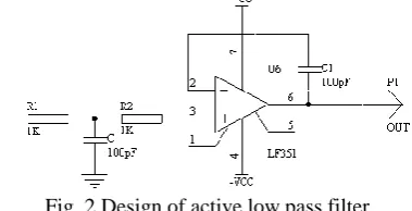
2. Filter LPF design
A filter consisting of an RC element and an operational amplifier is called an RC active filter whose function is to pass a signal within a certain frequency range to suppress or abruptly attenuate signals outside this frequency range. Can be used in information processing, data transmission, suppression of interference, etc., but due to operational amplifier band limitations, such filters are mainly used for low frequency range. According to the frequency range of choice, can be divided into low-pass (LPF), high-pass (HPF), bandpass (BPF) and band resistance (BEF) and other four filters.
Fig. 2 Design of active low pass filter
vice versa.The higher the order of the filter, the faster the rate of attenuation of the amplitude-frequency characteristics, but the more the number of nodes in the RC network, the more cumbersome component parameter calculation, the more difficult the circuit debugging. Any higher order filter can be implemented with a lower second order RC filter cascade.
An ideal filter should have a uniform and stable gain in the desired frequency band, and an infinite attenuation outside the passband. However, the actual filter has a certain difference from this, for which people use a variety of functions to approximate the frequency characteristics of the ideal filter, with the operational amplifier RC network composed of active filter has many unique advantages. Because there is no inductance element, so remove the inherent characteristics of the inductor, magnetic field shielding, loss, size and weight is too large and other shortcomings. As the operational amplifier gain and input impedance is high, the output impedance is low, it can provide a certain signal gain and buffer effect. This design can be a second-order RC active low-pass filter.
III.
SYSTEM
SOFTWARE
DESIGN
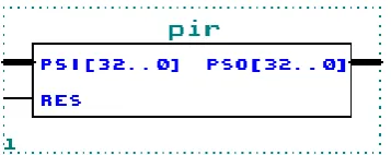
1. Phase increment register module
According to the previous calculations, the phase increment register requires 29 bits. The crosspoint of the phase increment register includes the reset terminal RES, the data input PSI (28: 0), and the data output PSO (32: 0). RES is active high, after reset, the PSO output is 0. PSO output high 4 bits total zero. In this design, the phase increment register is mainly stored in the frequency control data [12]. Figure 3 is the phase increment register module program debugging the correct results, Figure 3 is the module's function diagram. After the module is debugged correctly we have to proceed to the next step, and the most important step in this design is that the generation of the corresponding symbol is the sign of the phase increment register.
Fig. 3 Phase increment register
2. Phase increment register module
Because the accumulator requires 33 bits, if the general adder is used to achieve the cumulative, then there will be a very large carry delay, when the output frequency is high, it can not meet the requirements, so the class part of the pipeline structure, the 33-bit addition is divided into three levels of pipeline structure, each level is the 11-bit adder, this can greatly reduce the carry delay, it can meet the requirements of high-frequency output . Figure 4 is a pipelined port diagram. The pipeline adders are input for clock CLK, reset terminal RES, 33 bit wig data input ina (32: 0) and inb (32: 0) output data sum (32: 0), carry output cout.
3. Waveform memory module
The waveform memory is actually a two-port RAM. The waveform memory stores the data values of the 256-point sampled by the generated waveform. The change in the value of the address is changed because the address does not necessarily change continuously , So the output value is not continuous, in the same clock cycle, the address interval changes also caused the generation of waveform frequency changes. Each time the address value overflows, the output of one cycle is completed.
The two-port RAM is designed with IP cores. The ports are: the first address bus Wraddress [7: 0], the output data bus Q [7: 0], the clock Clka, the second address bus Rdaddress [7: 0] Input Data Bus Data [7: 0], Clock Clkb, Write Enable Wren. The address bus is connected to the output of the address register. The output data bus Q [7: 0] is connected to the I/O port of the CPLD as an input to the D/A converter.
IV.
SYSTEM
DEBUGGING
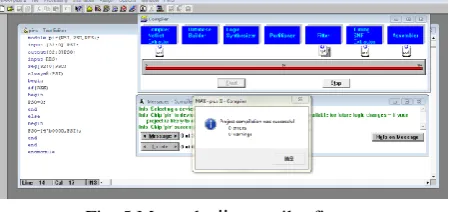
System software debugging is the use of Max+plus Ⅱ on several modules to debug the program, so the software debugging is the main software compiler and the function block program were written to verify the functionality of its executable. The module program to compile, compile and generate. V file, and then the module can be generated, and then the functional testing of the module.
Fig. 5 Max+plusⅡ compiler figure
The following simulation results for the 8-bit register, the frequency control word is 32, the clock cycle is 20ns when the simulation results. From the simulation waveform, the accumulator module meets the design requirements.
Fig. 6 Accumulator simulation diagram
The following simulation results for the 8-bit register, the frequency control word is 64, the clock cycle is 20ns when the simulation results. From the simulation waveform, the accumulator module meets the design requirements.
Fig. 7 Accumulator simulation diagram
The following is a result of sine wave simulation, but the internal waveform file is different. The following is a simulation of different waveform files waveform. As the simulation waveform is too large, so can not copy all the waveform down, the figure is just a schematic diagram, all the waveform in the design file sin.scf.
V.
CONCLUSIONS
Throughout the process, we have a certain understanding of the frequency synthesizer structure, principles and also have a wide range of understanding and learning of current frequency synthesis technology applications and the development of digital modulation technology, we are familiar with the use of frequency synthesis Technology for frequency synthesizers and a variety of digital modulators. In the process of the specific circuit design, the difference between theoretical and practical design also has a deeper understanding. This will be of great help to the future work and study, and it has laid a solid foundation for the further study of the application of frequency synthesizer, So I study relevant professional knowledge in depth, and be able to skillfully operate MAX+PLUS Ⅱ software. Through the use of CPLD chips and VHDL and Verilog hardware description language learning, I feel the convenience and flexibility of Verilog hardware description language, can improve programming skills rapidly, and recognize a lot of new design ideas. This brings me a great deal of help and far-reaching impact to the future. Although the research of this subject has achieved some gains but we need to improve many aspects, especially in the rapid development of information technology today, a variety of electronic products is made. A variety of technologies and methods are constantly improving. So the learning of electronic technical knowledge should also be constantly enriched and updated to meet the needs of work and society.
REFERENCES
[1] Cundiff S T, Ye J, Hall J L. Optical frequency synthesis based on mode-locked lasers[J]. Review of Scientific Instruments, 2001, 72(10): 3749-3771.
[2] Udem T, Holzwarth R, Hänsch T W. Optical frequency metrology[J]. Nature, 2002, 416(6877): 233-237.
[3] Shenghe W Q W Q S. Direct Digital Synthesizing Frequency Modulated Signal [J]. CHINESE JOURNAL OF SCIENTIFIC INSTRUMENT, 2000, 4: 027.
[4] Jridi M, Alfalou A. Direct digital frequency synthesizer with CORDIC algorithm and Taylor series approximation for digital receivers[J]. European Journal of Scientific Research, 2009, 30(4): 542-553.
[5] Hudson E R, Lewandowski H J, Sawyer B C, et al. Cold molecule spectroscopy for constraining the evolution of the fine structure constant[J]. Physical review letters, 2006, 96(14): 143004.
[6] Lin-pei X U Z Z, Hong-wei T Y Z. Design of High Frequency Sine Signal Generator Based on DDS [J].
Microcomputer Information, 2009, 5: 032.
[7] Huang K N, Huang Y P. Multiple-frequency ultrasonic distance measurement using direct digital frequency synthesizers [J]. Sensors and Actuators A: Physical, 2009, 149(1): 42-50.
[8] WU B, ZHU L, ZHAO J. Design and Simulation of Infrared Remote-Control Sending and Receiving Based on CPLD [J]. Computer Simulation, 2006, 8: 072.
[9] ZHANG M, WANG H, DING H. Design of Signal Generator Based on DDS Chip [J]. Instrument Technique and Sensor, 2010, 9: 021.
[10] QU Z, LIU S. Design Principles and Realization of High-speed Data Acquisition System Control Module