Effect of Concentration on Structure and morphological Properties of CZTS Thin Films
Synthesized by Sol-Gel Spin Coating method
Fatmah W.Redha1, Rafea A. Munef2 & Ali I. Salih3
1Department of Physics, College of Sciences, Kirkuk University, Kirkuk, Iraq. 2Department of Physics, College of Sciences, Kirkuk University, Kirkuk, Iraq. 3
Department of Physics, College of Sciences, Kirkuk University, Kirkuk, Iraq.
Received 10th September 2017, Accepted 14th October 2017
Abstract
In this present study, wurtzite CZTS nanocrystals have been prepared by a sol–gel route associated to spin coating for different molar concentrations in the precursor solution. The CZTS samples have been characterized structurally by X-ray diffraction (XRD), and the surface morphology of the thin films has been studied by using atomic force microscopes (AFM).XRD result reveal a wurtzite structure with preferred orientation along (100) to all sample, and the intensity of the peaks increased with the solution concentration increased, and the increasing molar concentrations led to an increase in the grain size, whereas dislocation density and micro strain decreases with the increase of molar concentrations. the secondary phases were observed due to the sulfur ratio used to prepare the thin film to avoid material decrease during preparation.AFM result shows. The roughness of the surface (RS) and the root mean square (RMS) values were increase with increasing of molar concentrations.
Keywords: Cu2ZnSnS4, Thin films, molar concentrations, Sol-Gel method, Structural Properties.
© Copy Right, IJRRAS, 2017. All Rights Reserved.
Introduction
Thin films chalcogen materials such as CuInS2
(CIS), CuInGa (S,Se)2 (CIGS) and CdTe are currently
produced at large scale and have already reached the commercialization stage. However, the scarcity of indium, gallium and tellurium in the earth crust will limit the future development of CIGS- and CdTe-based solar cells. In addition, the price of indium will increase in the near future because of the extensive use of indium in display technologies and opto-electronic devices. The toxicity of cadmium to health the scarcity be another problem to the development of CdTe-based solar cell.
To overcome this issue, it is necessary to develop new light absorber materials that are both nontoxic and easily available. Cu2ZnSnS4 (CZTS) with
an optimal direct band-gap of about 1.5 eV and a large absorption coefficient over 104 cm-1[1,2].CZTS is one of the most promising candidates as the absorber layers in thin film solar cells. It is composed of earth abundant elements which are copper, zinc, tin and sulfur [3,4]. All of them are nontoxic and this allows classifying the CZTS as future replacement for CIGS in the CIGS thin film solar cells.
CZTS thin films have been synthesized by various methods such as vacuum methods (sputtering,
Correspondence Fatmah W.Redha
E-mail: [email protected], Ph. +9194435 94140
thermal evaporation, spray pyrolysis) [5-10], non-vacuum methods (electro deposition, sol–gel, chemical bath deposition, successive ionic layer absorption and reaction, solvo thermal synthesis) [11-17]. Compared with the vacuum methods, the non-vacuum methods can attract a great deal of attention owing to their simpleness, low-price and no need of sophisticated instrumentation.
In present study, the sol–gel method with Spin-Coating technique was used for preparation CZTS film, because, this method is a very simple and low-priced process without requiring vacuum system , and has the distinct advantages in excellent composition control, and the ability to achieve atomic scale mixing of individual components. But The Effect of Concentration on Structure Properties of CZTS thin Films was not studied before, which was very important to improve the quality of films. In this paper, we report the Sol-Gel method to prepare wurtzite CZTS thin films directly on glass substrates, and investigate their structure, morphology Properties.
Experimental
CZTS thin films were prepared by Sol-Gel process from a solution with different molar concentrations of (0.125, 0.25, 0.375, 0.5)M. Precursor solution which consists of copper (II) acetate monohydrate, zinc (II) acetate dihydrate , tin (II) chloride dihydrate and thiourea, dissolved in2-methoxyethanol (50ml) as solvent and diethanolamine (5) mL as
International
Redha et al. 2017 ISSN: 2349 – 4891
stabilizer.
The resulting solution was stirred for (1) that room temperature, and then aged at room temperature for (24) h to get a clear and transparent homogeneous CZTS aqueous solution. The solutions compounds were filter with filter paper one time. A SLG substrate was treated by acetone, ethanol rinsed with deionized water, Then drying at(100 )°C for(30 ) min on a hot plate.
Sol–gel was dropped onto the rotating substrate at the beginning with (500) rpm for (10) s to (2500) rpm for (30) s. After deposition by spin coating, the film was dried with 200 °C for 10 min on a hot plate. The coating and drying processes were repeated (10) times to obtain thick films. The precursors were annealed for (1) h in air at(700)°C using an electric furnace. The structural properties of the films were characterized by X-ray diffraction (XRD) and Atomic Force Microscopy (AFM).
Results and Discussion X-Ray Diffraction
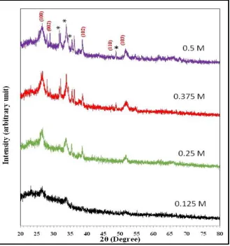
Figure I displayed the XRD patterns of CZTS thin films prepared by sol gel-Spin coating process with different molar concentrations of (0.125, 0.25, 0.375, 0.5)M, then annealed for (1) h in air at (700)°C. The XRD results showed that all the diffraction peaks
corresponded to the peaks of wurtzite-structured CZTS, indicating all the films had a hexagonal wurtzite structure. It can be seen that the major diffraction peaks at2θ=26.46°,27.95°,33.73°,38.60°, 51.57° can be attributed to the (100),(002),(101),(102, and (103), plans of wurtzite structure of CZTS [18-21].
It was observed that the intensity of the peaks increased with the solution concentration increased, which was caused by the increase of the film thickness. All the CZTS thin films shown a preferred orientation along the plan (100), and intensity of all this peaks
increasing with the increasing of the molar
concentrations, which means the increasing the amount of the material, the intensity of preferential orientation was increased indicating that the films crystallinity also has been improved. Although there was no standard card for wurtzite CZTS in JCPDS databases, This structure can be obtained from the wurtzite ZnS by replacing Zn(II) with Cu(I), Zn(II) and Sn(IV) [21]. Several peaks of the secondary phases (SnO2,SnS, ZnO) were observed
as shown in figure (1). This was due to the sulfur ratio used in preparing the thin films to avoid material decrease during preparation, It was also the process of annealing in the air impact in the emergence of these stages. This is consistent with published research [20,22,23].
Figure I
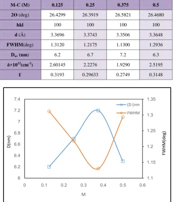
Table 1 showed the structural parameters of CZTS thin films. It can be observed the strongest peak at Bragg’s angle (2Ө= 26º) can be attributed to the (100) plane of the hexagonal CZTS, (FWHM) the width at half maximum intensity of the peaks which decreases with molar concentration increasing, Dav is the average grain
size was calculated from the (100) diffraction peak using Scherer formula [24]:
D =0.9λ/βcosθ ………(1)
λ is the X-ray wavelength, θ is the diffraction angle corresponding to the particular orientation, β is the width at half maximum intensity (FWHM) of the peak, The results indicated that the crystal quality of CZTS thin film was significantly improved with the increasing
in molar concentration.
δ is the dislocation density calculated from the Williamson and Small mans formula[25]:
δ=1/D2………..……….…(2) Exhibit a decrease with increasing molar concentration, which indicates that the high molar concentration reduced the crystal lattice imperfections. Larger D and smaller δ values mean better crystallization of the films.
Ɛ is the Micro Strain calculated from the formula in eq (3)[26]:
Ɛ= βcosθ/4…….…………(3)
which decreases with molar concentration increasing, As shown in figure II.
Table 1
Showed the structural parameters of CZTS thin films
Figure II
Grain size and full width of half maximum for CZTS thin films
Table 2 shows the values of lattice constants for all thin CZTS thin films with (0.125,0.25,0.375.0.5) M,
and for the highest peak (100). It is compatible with the derivative card for CZTS installation [27].
0.5 0.375 0.25 0.125 M-C (M) 26.4680 26.5821 26.3919 26.4299
2Ө (deg)
100 100 100 100 hkl 3.3648 3.3506 3.3743 3.3696
d (Å)
1.2936 1.1300 1.2175 1.3120 FWHM(deg) 6.3 7.2 6.7 6.2
Dav (nm)
2.5195 1.9290
2.2276 2.60145
δ×1012
(cm-2)
0.3148 0.2749 0.29633 0.3193 Ɛ 1.1 1.15 1.2 1.25 1.3 1.35 6 6.2 6.4 6.6 6.8 7 7.2 7.4
0 0.1 0.2 0.3 0.4 0.5 0.6
Redha et al. 2017 ISSN: 2349 – 4891
Table 2
The values of lattice constants for all CZTS thin film
Morphological properties (AFM)
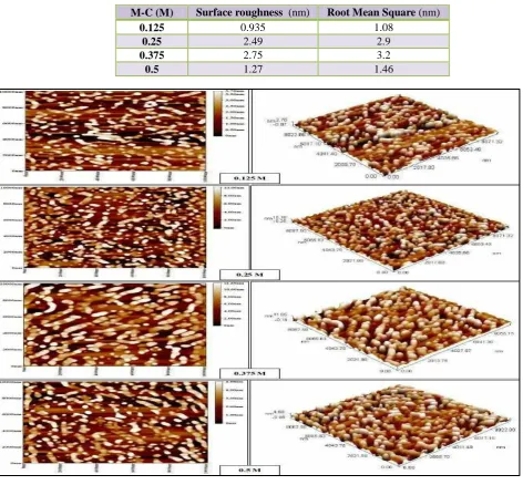
Using the Atomic Force Microscope (AFM), the effect of the molaric concentration on the nature and crystalline structure of the CZTS thin films was studied.
Table (3) shows the surface roughness (RS) and the root mean square (RMS) values, it was indicated that the films have good homogeneous crystalline and with smooth surface, as shown in figure III.
Table 3
Surface roughness and root mean square of CZTS thin films
Figure III
Shows the AFM images 2D & 3D of CZTS thin films, the grains are orthogonal to the film surface indicating that the film grows perpendicularly to the substrate.
𝒄(Å)
𝒂(Å)
M-C(M)
6.3388 3.8387
Card(Cu2ZnSnS4)
6.7446 3.8939
0.125
6.7541 3.8995
0.25
6.7066 3.8721
0.375
6.7350 3.8885
0.5
Root Mean Square (nm) Surface roughness (nm)
M-C (M)
1.08 0.935
0.125
2.9 2.49
0.25
3.2 2.75
0.375
1.46 1.27
Conclusion
In the present work, CZTS thin films were deposited by a simple and cheap deposition technique, namely Sol gel-Spin coating method for different molar concentrations in the precursor solution. The X-ray diffraction showed that films have a polycrystalline structure in Wurtzite phase with an orientation to the (100) crystallographic orientation. The intensity of this peak and grain size were increasing, therefore leads to decrease in Full Width at Half Maximums (FWHM) of peak With the increase in molar concentration. Surface morphological study showed that increase ingrain size with increasing molar concentration.
References
1. S.Kumar, A. Kumar, and V. Dutta. "Deposition of kesterite Cu2ZnSnS4 (CZTS) thin films by spin
coating technique for solar cell application." Energy Procedia 33): 198-202. (2013).
2. H.Katagiri, K.Saitoh, T.Washio, H.Shinohara, T. Kurumadani, andS. Miyajima." Development of thin film solarcell based on Cu2ZnSnS4 thin
films. Solar Energy Materials and Solar
Cells". 65(1), 141-148. (2001).
3. C.Wadia, A. P. Alivisatos, and D. M. Kammen. "Materials availability expands the opportunity for
large-scale photovoltaics
deployment." Environmental science & technology 43.6 2072-2077.(2009)
4. D. BMitzi, O. Gunawan, T. K.Todorov, Wang, K., &S. Guha."The path towards a high-performance solution-processed kesterite solar cell. Solar Energy Materials and Solar Cells". 95(6), 1421-1436. (2011).
5. T.Tanaka, T. Nagatomo, D. Kawasaki, M. Nishio, Q. Guo, A. Wakahara&H. Ogawa. "Preparation of Cu2ZnSnS4 thin films by hybrid sputtering. Journal
of Physics and Chemistry of Solids". 66(11), 1978-1981.(2005).
6. F.Liu,Y. Li, K. Zhang,B. Wang,C. Yan, Y. Lai, &Y. Lai,. In situ" growth of CuZnSnS4 thin films by
reactive magnetron co-sputtering". Solar Energy
Materials and Solar Cells. 94(12),
2431-2434.(2010).
7. H. Nozaki, T.Fukano, S. Ohta, Y. Seno, H. Katagiri, &K. Jimbo." Crystal structure determination of solar cell materials: Cu2ZnSnS4 thin films using
X-ray anomalous dispersion". Journal of Alloys and Compounds. 524, 22-25.(2012).
8. P. A.Fernandes, P. M. P. Salomé, and A. F. Da Cunha. "Growth and Raman scattering characterization of Cu2ZnSnS4 thin films".Thin
solid films 517.7: 2519-2523.(2009).
9. N. Nakayama, and K. Ito. "Sprayed films of stannite Cu2ZnSnS4." Applied Surface Science 92: 171-175.(1996).
10. B.A.Schubert, B.Marsen, S.Cinque, T.Unold, R. Klenk, S. Schorr, &H. W. Schock. "Cu2ZnSnS4
thin film solar cells by fast
coevaporation". Progress in Photovoltaics: Research and Applications. 19(1), 93-96.(2011). 11. K.Tanaka, M.Oonuki, N.Moritake, &H. Uchiki,."
Cu2ZnSnS4 thin film solar cells prepared by
non-vacuum processing". Solar Energy Materials and Solar Cells. 93(5), 583-587.(2009).
12. A.Fischereder, T.Rath, W.Haas, H. Amenitsch, J.
Albering, D. Meischler, &G. Trimmel.
"Investigation of Cu2ZnSnS4 formation from metal
salts and thioacetamide". Chemistry of materials. 22(11), 3399-3406.(2010).
13. S. S.Mali, B. M.Patil, C. A. Betty,P. N. Bhosale, Y. W. Oh, S. R. Jadkar …&P. S. Patil."Novel synthesis of kesterite Cu2ZnSnS4 nanoflakes by successive
ionic layer adsorption and reaction technique: characterization and application". Electrochimica Acta, 66, 216-221.(2012).
14. Y.Wang, J.Ma, P.Liu, Y. Chen, R. Li, J. Gu... &X. Gao. "Cu2ZnSnS4 films deposited by a
co-electrodeposition-annealing route". Materials letters. 77, 13-16.(2012).
15. N. M.Shinde, D. P. Dubal, D. S. Dhawale, C. D. Lokhande, J. H. Kim, &J. H. Moon." Room
temperature novel chemical synthesis of
Cu2ZnSnS4 (CZTS) absorbing layer for
photovoltaic application". Materials Research Bulletin. 47(2), 302-307.(2012).
16. S. SMali, P. S. Shinde, C. A. Betty, P. N. Bhosale, Y. W.Oh. &P. S. Patil."Synthesis and characterization of Cu2ZnSnS4 thin films by SILAR
method". Journal of Physics and Chemistry of Solids. 73(6), 735-740.(2012).
17. Z.Yan, A.Wei, Y.Zhao, J.Liu, &X. Chen. "Growth of Cu2ZnSnS4 thin films on transparent conducting
glass substrates by the solvothermal
method". Materials Letters.111, 120-122.(2013). 18. H.Guan, H. Hou, F. Yu, & Li, L." Synthesis of
wurtzite Cu2ZnSnS4 thin films directly on glass
substrates by the solvothermal method". Materials Letters. 159, 200-203(2015). .
19. I. B.Vashistha, M. C.Sharma, R.Sharma, &S. K. Sharma." Formation of Kestarite and Wurtzite Structure of Cu2ZnSnS4 Thin Films by Chemical
Bath Deposition (CBD) Method for Solar Cell Application. (2015).
20. H.Jalal, A.I.Salih, R.A.Munef ,"Effect of Annealing Temperature on the Structural Properties of Cu2ZnSnS4 Thin Films Prepared by Sol-Gel
Method". Journal of Recent Research and Applied Studies.ISSN:2349-4891.(2016).
21. J.H.N.Tchognia, Y.Arba, K. Dakhsi & B. Hartiti. "Solution-based deposition of wurtzite copper zinc tin sulfide nanocrystals as a novel absorber in thin film solar cells." Optical and Quantum Electronics.48.4: 1-6(2016).
22. T.T.Mau, and K. H. Kim. "Synthesis of Cu2ZnSnS4
Redha et al. 2017 ISSN: 2349 – 4891
23. E.M.Mkawi,K.Ibrahim,M. K. M.Ali,, & A. S.Mohamed. "Dependence of copper concentration on the properties of Cu2ZnSnS4 thin films prepared
by electrochemical method". Int. J. Electrochem. Sci, 8, 359-368.(2013).
24. Y. B. Kumar, G. S. Babu, P. U. Bhaskar and V. S. Raja." Solar Energy Materials and Solar Cells". 93(8), 1230-1237.(2009).
25. J. Henry, K. Mohanraj and G. Sivakumar, Journal of Asian Ceramic Societies. 4(1), 81-84,(2016). 26. P. Kathirvel, D. Manoharan, S. M. Mohan and S.
Kumar, J Optoelectron Biomed Mater, 1,25-33,(2009).