Method for determining the adhesion force
between graphene and copper
Evgeny Victorovich Boyko1,2,*, Ilya Alexeevich Kostogrud2, Dmitry Vladimirovich Smovzh1,2, Mikhail Sergeevich Skirda1, and Pavel Evgenyevich Matochkin1
1
Novosibirsk State University, Pirogov str. 2, 630090, Novosibirsk, Russia
2
Kutateladze Institute of Thermophysics SB RAS, Acad. Lavrentiev Ave. 1, 630090, Novosibirsk, Russia
Abstract. The paper presents the technique of qualitative assessment of the strength of graphene layers adhesion to the surface of a copper substrate, where they are formed. The technique uses a complex of approved analytical methods: electron backscatter diffraction (EBSD), Raman spectroscopy and optical microscopy. The technique was tested on multilayer graphene grown on a copper grain with crystal orientation (111). The presented method can be used to assess the effectiveness of the methods of graphene transfer from grains with different crystal orientation.
1 Introduction
Today, graphene is one of the most promising materials: both in terms of basic research and practical application. Manifestation of properties of this two-dimensional carbon structure in the form of high mobility of charge carriers [1], thermal conductivity [2], strength [3], and low gas permeability [4] allows its use in various scientific and technical fields. Graphene can be synthesized in many ways [5], but the most widely spread method is chemical vapor deposition (CVD). In this method, copper (Cu) is most often used as a catalytic surface, where graphene grows [6 - 8]. However, in most applications it is necessary to transfer graphene from a copper substrate to some other surface. Among all transfer procedures, two main classes can be distinguished: using chemical etching of copper [9] and mechanical separation of copper from graphene [10]. The obvious disadvantage of the first class is the irreversible process of destruction of the copper catalytic substrate in the process of graphene transfer. The second class of these methods has no such disadvantage, but the question about the strength of adhesion in graphene– copper systems arises. To minimize the number of defects associated with destruction during graphene transfer, the adhesion force with copper should be minimized. The effect of catalytic substrate on synthesized graphene is widely reported in the scientific literature. Thus, it is found in [11] that graphene forms predominantly on copper (Cu) crystallites with (111) and (100) orientations. However, under the same synthesis conditions, on the planes with Miller indices (111), graphene has a uniform shape. In the zones of copper with the
*
family of planes (100), the opposite situation occurs, and graphene has a pronounced discontinuous structure. In addition to influencing the morphology of graphene, the catalytic surface can change its electrical properties. For example, it is shown in [12] that the electrical resistance of graphene films depends monotonically on the roughness degree of copper foil, where it is synthesized. Using this fact and performing some preliminary treatments of copper surface, the authors of this work were able to reduce the electrical resistance of graphene to 210 Ohms/sq, and increase the mobility of charge carriers up to 5450 cm2/(V⋅s) after transfer to the silicon (Si) substrate. Less information concerning the influence of copper crystalline orientation on the adhesion force between the substrate and graphene can be found in scientific literature. Techniques, which allow determination of this value, are difficult. A confirmation of this can be found in [13], where the nano-scratch method was used to determine the adhesive energy between graphene and copper foil [14]. Its main idea is to use an atomic-force microscope with a special tip, which allows measuring the force required to separate a graphene film from the substrate. The simpler and equally reliable methods are not available now. This work deals with the solution to this problem.
2 Experiment
Graphene was obtained by chemical vapor deposition. A detailed description of the synthesis procedure is given in [15]. The obtained samples were certified using a HoribaJobinYvon T64000 Raman Spectrometer (514.5 nm). In the spectra obtained, the D, G, 2D peaks, characteristic of graphite structures, were analyzed. The number of graphene layers on the substrate and their defectiveness were determined by the shape of the 2D peak and ratio of intensities of the D, 2D, and G peaks.
Orientation and size of the copper grains were determined by the EBSD method using a Hitachi S-3400N scanning electron microscope. Graphene transfer is performed using polyethylene terephthalate/ethylene vinyl acetate polymer. A detailed description of this process is presented in [16]. After the stage of transfer, the copper substrate was oxidized at 190°C in air and examined using an Olympus BX51M optical microscope.
3 Results and discussion
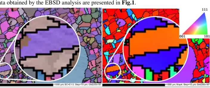
Data obtained by the EBSD analysis are presented in Fig.1.
Fig. 1. EBSD in Euler angles (on right) and Miller indices (on left).
occupied by crystallographic planes with Miller indices (111) (blue zone in Fig. 1), another, the central area, is intermediate between the (001) and (101) planes (orange zone in Fig. 1). Also, a Raman spectrum and optical microscopy image were obtained for the selected region (presented in Fig. 2 and Fig. 3).
1200 1400 1600 1800 2000 2200 2400 2600 2800 40
60 80 100 120 140 160
2D G
In
te
n
s
it
y
Raman shift, cm-1
Orange zone Blue zone
D
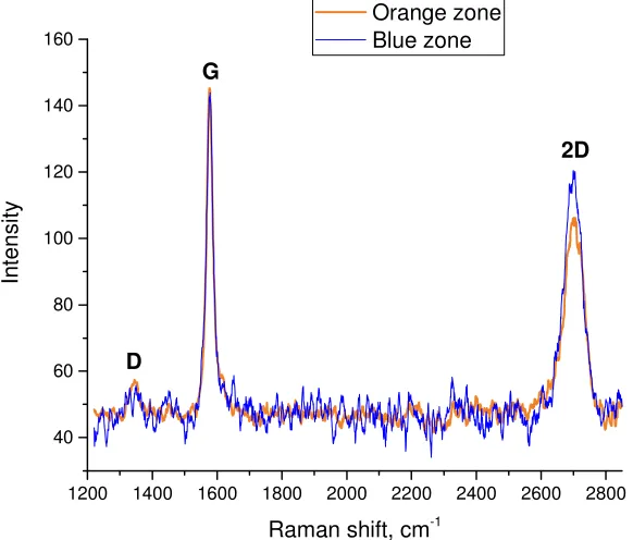
Fig. 2. Raman spectrum of the studied regions of the copper substrate with graphene (the first graph – blue zone in Fig.1, the second graph – orange zone in Fig.1)
The Raman spectrum was registered before the procedure of graphene transfer, while microscopic investigation was done after. To determine the areas containing remaining graphene, the sample was oxidized in air: at this stage, one of graphene properties was used, namely, its low gas permeability [4]. There is no contact of copper with oxygen in the presence of graphene, so after the procedure of substrate oxidation, it is easy to detect the places with graphene remaining after the stage of its transfer (Fig. 3).
As a result of Raman spectrum analysis, the position and FWHM of the G and 2D peaks were determined. For the first graph (Fig. 2 - blue line) – peak G: position is 1577 cm-1, FWHM is 27 cm-1. Peak 2D: position is 2700 cm-1, FWHM is 60.4 cm-1. The ratio between these peaks is ⁄ 0,76.
For the second graph (Fig. 2 - orange line) – peak G: position is 1577 cm-1, FWHM is 22 cm-1. Peak 2D: position is 2701 cm-1, FWHM is 61.1 cm-1. The ratio between these
peaks is ⁄ 0,6.
Thus, we can conclude that graphene, located in this region, is multi-layered (≥ 3 layers). The ratio of intensities of the D and G peaks allows us to estimate the degree of “imperfection” (amount of defects) of synthesized graphene. In our case, the intensity of peak D is at the noise level, the maximal ratio is ⁄ 0,09 in the blue zone and ⁄ 0,11 in the orange zone, which indicates the slightly disordered graphene structure and the number of defects in it is above the average (for comparison, the same ratio for single-layer graphene with low defectiveness is ≈ 0.063).
It is convenient to trace the dependence of adhesion by calculating the ratio of the area covered by remaining graphene to the total grain area (S1/S2). The area was calculated using
ImageJ software. For example, the studied region (see Fig. 3, the right part) consists of a copper grain, in the center of which there is a strip with different crystal orientation. The microscopy photograph of this region was pretreated in order to obtain the optimal contrast and brightness for the automated search for bright spots: zones of copper that were not oxidized due to the presence of a graphene film on them. Bright spots, which did not contain remaining graphene, but noted by the search algorithm, were screened out manually. Thus, the microscopy photograph was processed virtually without data loss. For each region, the area, number of graphene spots, which it contains, and their areas were calculated individually (Fig. 4).
Fig. 4. An example of calculating the total area occupied by graphene spots (denoted by ordinal numbers).
Ultimately, the share occupied by the graphene spots on the studied copper grain was calculated. Below, there is distribution over the studied region (Fig. 5).
It can be seen from Fig. 4 and Fig. 5 that areas covered with graphene are different for the areas with different crystal orientations. At that, based on the data of optical microscopy
of Fig. 4, it can be concluded that copper roughness does not change. Thus, the main factor
determining the quality of graphene transfer in our case is the crystalline orientation of copper. Based on the analyzed data, it can be concluded that interaction of the graphene coating with the (111) plane is stronger than with (310).
4 Conclusions
Measuring the adhesion force of various surfaces is a time-consuming problem, which does not always justify the efforts spent on its solution. A simple method that can quickly provide information on intermolecular interaction energy in various systems (for instance, metal-polymer) can greatly facilitate the experiments aimed at studying and testing the regimes of graphene transfer from the catalytic growth substrates to other surfaces. One of these methods was created due to the work presented, and it can serve for quick and reliable qualitative assessment of adhesion degree in the graphene-copper and graphene-polymer systems.
Using this technique and EBSD analysis, it is possible to compare qualitatively the adhesion force between graphene and crystalline grains with various Miller indices. Investigation of the forces of interaction between copper and graphene layers growing on it will make it possible to develop the technologies for more efficient transfer of graphene to a polymer using the methods of mechanical separation.
The work was financially supported by the Russian Ministry of Education and Science (Unique identifier of applied scientific research (project) RFMEFI60417X0157).
References
1. K.S. Novoselov, A.K. Geim, S.V. Morozov, D. Jiang, Y. Zhang, S.V. Dubonos, I.V. Grigorieva, A.A. Firsov, Science, 306, 666 (2004)
2. S. Ghosh, D.L. Nika, E.P. Pokatilov, A.A. Balandin, New J. Phys., 11 (2009) 3. C. Lee, X. Wei, J.W. Kysar, J. Hone, Science, 321, 385 (2008)
4. Y. Su, V.G. Kravets, S.L. Wong, J. Waters, A.K. Geim, R.R. Nair, Nat. Commun., 5, (2014)
5. S.S. Shams, R. Zhang, J. Zhu, Mater. Sci.-Poland, 33, 566-578 (2015)
6. A. Guermoune, T. Chari, F. Popescu, S.S. Sabri, J. Guillemette, H.S. Skulason, T. Szkopek, M. Siaj, Carbon, 49, 4204-4210 (2011)
7. M. Losurdo, M.M. Giangregorio, P. Capezzuto, G. Bruno, Chem. Phys., 13, 20836-20843 (2011)
8. X. Li, L. Colombo, R.S. Ruoff, Adv. Mater., 28, 6247-6252 (2016) 9. N. Yoshihara, M. Noda, Chem. Phys. Lett., 685, 40-46 (2017)
10. M. Marchena, F. Wagner, T. Arliguie, B. Zhu, B. Johnson, M. Fernández, T.L. Chen, T. Chang, R. Lee, V. Pruneri, P. Mazumder, 2D Mater., 5 , 1-25 (2018)
11. L. Zhao, K.T. Rim, H. Zhou, R. He, T.F. Heinz, A. Pinczuk, G.W. Flynnd, A.N. Pasupathy, Solid State Commun., 151, 509-513 (2011)