ASIC Implementation of Three Stage Data
Path Logic Structure
Subha Sri. Thiruveedhi
1, K.Tharun Teja
2,Nedunuri. Sreekar
3Assistant Professor, Dept. of ECE, CVR College of Engineering, Hyderabad, Telangana, India1 B.Tech Student, Dept. of ECE, CVR College of Engineering, Hyderabad, Telangana, India2
B.Tech Student, Dept. of ECE, CVR College of Engineering, Hyderabad, Telangana, India3
ABSTRACT: In the embedded system applications the RISC-ARM architecture is proven to be very much useful by providing several advantages. The three stage pipeline structure i.e., ARM7 TDMI architecture is the highest sold chip till now in comparison with all other micro controllers. The ARM7 has become so popular due to its data path design consisting ALU, Barrel shifters, CPSR register. This architecture allowed optimised assembly language coding for several applications resulting low power designs. The paper scope includes the study of 3-stage pipeline instruction set and implementing the ALU. The barrel shifter will be implemented to optionally shift one of the input before going to the ALU. In this paper, 3-stage data path structure consists of ALU, Barrel shifters, CPSR register unit blocks will be implemented in VHDL. In the ASIC Digital design the RTL Compiler and SOC Encounter are used for simulation and synthesis purpose and finally we obtain the GDSII file. This paper uses TSMC 45nm technology libraries for implementation. RTL Complier tool will be used for functional simulation (RTL SCHEMATICS) and verification of data path structure. SOC ENCOUNTER tool will be used to synthesize the blocks. This data path structure which can be used for different applications like Military, Automation and Consumer Electronics.
KEYWORDS: RISC, Three Stage Pipeline Structure, Data path Logic, ALU, Barrel shifter, CRSR register Unit and ASIC.
I. INTRODUCTION
In olden days performing any operation by using embedded systems includes a tedious process of connecting external devices and also more expensive [2]. So by using advanced technology we implement them on ASIC that have all the required devices present in it and are also facilitated with placement, partitioning, routing and finally fabricated on IC, this simplifies the operation. Today several complex embedded systems require soft processor core on ASIC by which they perform multiprocessor core based applications at very high speed. The three stage pipeline structure of ARM7 TDMI architecture is very popular and implementing in ALU facilitates the ARM assembly to work on ASIC. To achevieve better communication services with fast performance [1], less area and low power the 3-stage pipeline structure is implemented on ASIC.
II. RELATEDWORK
III.THREESTAGERISCPHILOSOPHY
The main feature of three stage pipeline structure is Architectural Simplicity which allows Very Small Implementations which result in Very Low Power Consumption and it occupies very less area on Silicon die.RISC (Reduced Instruction Set Computing) philosophy become very popular due to its load/store architecture, large uniform register file, and Uniform and fixed-length instruction fields and developed by the Advanced RISC machines. High code density is another major requirement since embedded systems have limited memory due to cost and/or physical size restrictions. High code density is useful for applications that have limited on-board memory, such as mobile phones and mass storage devices [3].The three stage pipeline sturcture and internal structure of pipeline logic is shown in the below figure 1.1 & 1.2.
Fig: 1.1 Three Stage Pipeline Structure Of Data Path Logic
Fig: 1.2 Internal Structure Of Three Stage Pipeline Structure Of Data Path Logic
IV.THREESTAGEPROGRAMMINGMODEL
User, FIQ (Fast Interrupt Request), IRQ (Interrupt Request), SVC (Supervisor), ABT (Abort), UNDEF (Undefined), SYS (System).
Table 1: Exception Types, Sorted By Interrupt Vector Addresses
V. THREESTAGEDATAPATHLOGICSTRUCTURE
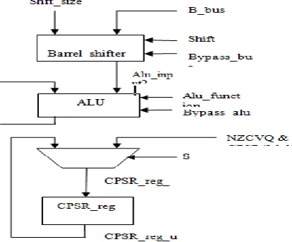
The three stage pipeline structure of ARM7 TDMI core has Von Neumann architecture, with a single 32-bit data bus carrying both instructions and data. Only load, store and swap instructions can access data from memory. As explained, the ARM architecture consists of the three fundamental blocks. Data Path (ALU, Barrel Shifter, CPSR register), Controller, ROM. In this project, the crucial part of data path is implemented. The following figure 1.3 shows the implemented blocks.
Fig 1.3 Implemented Blocks of Three Stage Data Path Structure
BARREL SHIFTER BLOCK
The data path uses this barrel shifter to shift any data as per the instruction with the given amount of shift given by controller, if we want to avoid that barrel shifter then just give the signal Bypass_bs, coming from controller. The two inputs coming are the amount of size and the data, and then result will be Alu_input2 that is shifted data [1].
Shft_size : Shift amount given by the mux i.e. either Rs, or inst 0 & (11:8) or inst (11:7) B_bus: Data coming from above mux i.e. Rm or Rn or Mul _l or Mul_H.
Fig 1.4 Barrel Shifter
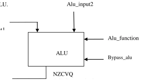
ALUBLOCK
The Data path uses this ALU for all Arithmetic and Logical operations with the signals given by the controller i.e. Alu_function decides the function to be performed and Bypass_alu decides to use the ALU or just bypass the ALU. The two inputs Alu_input1 and Alu_input2 are the data for some function coming from various other units in data path.
Alu_input1, Alu_input2: Data’s coming from Op4 mux and Barrel shifter. Alu_function: Decides the function.
Bypass_alu: Signal to bypass ALU.
Fig 1.5 Arithmetic and Logic Unit
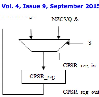
CPSR REGISTER BLOCK
The Data path uses this mux for updating the flag register using the signal coming for the controller i.e. if we have an S bit in our instruction then controller will give signal. Then this will be updated. N, Z, C, V, Q are the flags for Negation, Zero, Carry, Overflow, Saturation flags.
Barrel_shifter Shft Bypass_alu B_bus
Shft_size
Alu_in2
ALU
Alu_function
Bypass_alu
Alu_input1
NZCVQ
Fig 1.6 CPSR Register
The CPSR is a 32bit register in addition to the 16 general purpose registers. The CPSR has flag and control bits in it. The following figure illustrates the bit positions of various control or flag bits of CPSR.The CPSR are divided into 4 fields, each of 8 bits size. They are Flag, status, extension and control fields. In the present versions of ARM the status and extensions field’s bits are reserved for future use. If flag up date option is enabled1 then the flag bits will be
changed as described below. Remember that flag bits are only affected when such option is chosen in the instruction; otherwise flag bits will preserve their old values. N – Negative flag. This bit is set when the 31 bit (most significant bit) of result is one, otherwise it is reset
Z – Zero flag. This bit set if the result is zero, otherwise it is reset
C – Carry flag. This bit is set when there is a carry out of addition, and no barrow for subtraction, otherwise it is reset V – Overflow flag. This bit is set when there is overflow in signed arithmetic operations
The I and F bits correspond to interrupt masking and the T bit tells the thumb state (whether the processor is in normal mode or thumb mode).
The least significant five bits of CPSR indicate the mode in which processor is currently operating. Except in user mode in all other modes it is possible to write appropriate value in these bits for changing to any other mode. The mode also can be changed when exception or interrupt occurs.
Fig 1.7 32 Bit CPSR Register Format
VI.EXPERIMENTALRESULTS
REFERENCES
Fig 1.8 RTL Compiler Simulation Results of 3 – Stage Data path Structure. a) RTL Schematic of ALU, b) RTL Schematic of Barrel Shifter, c) RTL Schematic of Complete Data path, d) Net power usage of 3-Stage Data path Structure.
a) b)
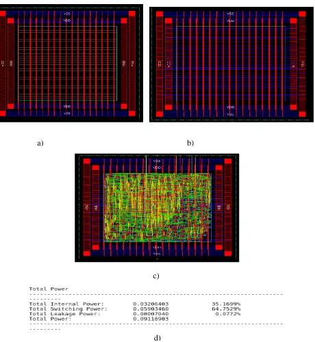
Fig 1.9 SOC Encounter Synthesis Results of 3 – Stage Data Path Structure. a) Power plan with add rings & add stripes, b) 3-stage Data Path structure after placing standard cells, c) GDS II file of complete Data Path, d) Total power usage of 3-Stage Data Path Structure.
In fig 1.9 we can see the SOC ENCOUNTER, some series of steps. Floor planning defines adding of rings (VDD, GND) and strips (covering the interior core). Performing the placement (with the help of standard cells), routing (special route and nano route) which performs all connections between the blocks, defining the clock and checking the
a) b)
c)
pre clock synthesis and post clock synthesis reports and finally verifying the geometry conditions and connectivity conditions and save the file as GDS II file which will be given to the industry for IC fabrication.
VII. CONCLUSION
Three stage Data path RISC processor core were implemented in the ASIC based System On Chip applications. All the 32-bit instructions were implemented with single cycle data path and random logic based instruction decoder. The instructions of Data processing, Arithmetic, Branch instructions, Logical and compare were implemented. The data path was implemented with ALU, Barrel Shifter. Alternatively the Data path design can also be implemented on recent ASIC technologies which are presently using in industries for better power usage and to achieve higher speeds. Three stage Data Path logic structure ARM cores can be extended by 5- stage, 7-stage and 9-stage processors also.
REFERENCES
[1] B T Sundari1, T. Surender Reddy2, Dr. Laxminarayana G, “IMPLEMENTING THE ARM7 SOFT CORE PROCESSOR IN FPGA”, in IJCER , Vol 2, Issue 2, April 2013.
[2] Alex Heunhe Han, Young-Si Hwang, Young- Ho An, So-Jin Lee, Ki-Seok Chung “Virtual ARM Platform for Embedded System [3] J. O. Hamblen, T. S. Hall “Using System-ona- Programmable-Chip Technology to Design Embedded Systems” IJCA, Vol. 13, No. 3. [4] Andrew N.sloss, Dominic symes, Chris Wrig ARM System Developer’s Guide designed and optimized system software.