Synthesis of MIMO Architecture Designed Using
Adiabatic Logic at 45nm Technology
1
S.Bharani Kumar,
2S.Janani
1,2Dept. of Applied Electronics, A.V.C. College of Engineering, Mannampandal, Tamil Nadu, INDIA
Abstract
This project aimed to develop an ASIC to achieve the power consumption and area minimization. In this paper we present an
energy efficient programmable hardware accelerator that targets
multiple input multiple output decoding tasks orthogonal frequency
division multiplexing system. The work is motivated by the adoption of MIMO and OFDM by almost all existing and emerging
high speed wireless data communication systems. The accelerator
was fabricated in 45-nm CMOS technology and occupies a core area of 2.48mm2. It delivers over all programmability across different wireless standards (Wi-Fi, 3G-Long term evolution, and WiMAX) as well as different MIMO decoding algorithms (i.e., minimum mean square error, singular valued decomposition and maximum likelihood) with extreme energy efficiency. The energy efficiency of MIMO decoder accelerator chip was compared against dedicated application specific integrated circuits for 4*4 singular value decomposition, 4*4 QR decomposition, and 2*2 minimum mean square error decoding. Here we using two logic irreversible and reversible or adiabatic logic. We have to replace the adiabatic or reversible logic gates instead of existing irreversible logic in
MIMO decoder architecture.
Keywords
Multiple Input Multiple Output (MIMO) Decoder, OFDM,
ASIC
I. Introduction
Now days, most high-speed wireless communication standards adopt both multiple-input-multiple-output (MIMO) and
Orthogonal Frequency Division Multiplexing (OFDM) operation.
This applies to small-scale wireless data networks, such as the 802.11n wireless LAN standard [2], as well as large-scale cellular systems such as WiMAX [3] and Long Term Evolution (LTE) [4] (including its enhanced version LTE-A [5]) that are considered 4G cellular candidates. In OFDM, a wideband frequency selective fading channel is divided into several independent narrowband flat-fading.
In addition to the construction of these sub channels at the transmitter, the receiver hardware is required to independently
perform channel processing (estimation and equalization) for
each and every one of these sub channels. Similarly, MIMO
operation requires parallel processing for multiple data streams
at the transmitter and, more importantly, at the receiver where the MIMO decoder is notorious for being one of the most processing-intensive blocks.
A MIMO decoder is the receiver component that separates the Nss transmitted data streams from the signals received on the
Nrxreceive antennas. Most, if not all, of the MIMO decoding operation is matrix and vector intensive. For an OFDM system, this processing is repeated for every sub channel.This fact serves as the main motivation for the proposed solution. A programmable
hardware solution focused on the unique MIMO decoding operations of a MIMO system can help drive down nonrecurring
engineering costs, can facilitate system upgrades to take advantage
of emerging algorithms and can help minimize hardware
duplications in system-on-a-chips (SoCs) that support multiple standards. Through sacrificing part of the performance and/or cost constraints, a multimode MIMO decoder can be designed to target multiple communication standards. Several reconfigurable. In this paper, the authors extant an IC implementation for a
MIMO decoder accelerator (or simply a MIMO accelerator) in
45-nm CMOS technology. The MIMO accelerator is a software-programmable device that specializes in MIMO decoding, and
MIMO signal processing for OFDM systems.
II. Exixting System
Each individual dedicated Solution architecture (Decoder architecture for each wireless communication standard like Wi-Fi, LTE, Wi-Max) presented in the communication Protocol’s. A system designer chooses a single MIMO decoding algorithm to be used by the system subject to the need to satisfy the specifications
of the standard at hand. A hardware engineer then implements the chosen algorithm with constraints on complexity.
III. Proposed System
In this paper we are implementing the Integrated Solution Architecture presented like SoC architecture of Decoder in the
communication protocols. A programmable hardware solution focused on the unique MIMO decoding, operations of a MIMO
system can help drive down nonrecurring engineering costs. It can facilitate system upgrades to take advantage of emerging algorithms and can help minimize hardware duplications in
system-on-a-chips (SoCs) that support multiple standards.
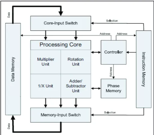
A. MIMO Decoder Accelerator
MIMO decoding is based on extensive matrix processing. Linear decoders (such as MMSE and ZF decoders) basically invert a
channel matrix. Increase wireless system performance without increasing power consumption.
MIMO algorithm sends data over two or more antennas and
received via multiple antenna as well. Complex number vector based processor that tasks on complex vector operands of length Nrx used in the MIMO system. Each individual dedicated
solution architecture (decoderarchitecture for each wireless
communication standards like Wi-Fi, LTU, WiMAX) presented
in the communication protocols.
Memory blocks are phase memory instruction memory and data memory. The memory-input switch performs the related work, but in the opposite direction. It takes the outputs of the processing
units and properly packages them so as to write all data associated
with the given OFDM subcarrier into the appropriate memory location the core-input switch is a two level multiplexing circuit that selects and properly arranges the complex vectors needed by the processing core. Whether they are rowvectors, column vector, matrix diagonal combination.
B. OFDM
Orthogonal Frequency Division Multiplexing, Wide frequency band used intentionally, Eliminates problems associated with OFDM (i.e.: Multipath), Potential data rates to 155 Mbps (and beyond), Ideal for wireless high-speed networking, Why OFDM? Very good bandwidth efficiency, this means high data rates. Robust against multipath fading Employ the latest DSP and ASIC technology Randomize (pre-whiten) the input data, Combine
channel estimation with forward error correction.
C. ASIC (Application Specific Integrated Circuits)
First we going to synthesis the design of our RTL module (MIMO decoder), let see process of cadence implementation. To open code of acs and click the display button. By using cadence RTL compiler, we go to synthesis the design .click the synthesis net list
option and copy the ACS (accumulator carry selector) then right
click to select open terminal. To enable the rc-gui code to enter and checkout license for RTL compiler ultra-seconds to execute further steps.Enter all the synthesis procedure step for synthesis our design. Here we use 45nm library, then we find HDL search path and read HDL vhdl code. Then we going to elaborate the each design code and verify the each design of acs0 to acs7.
Enter the code Synthesis to generic and synthesis succeeded.
Then enter the code for synthesis of mapped and synthesis
succeeded. write_hdl_genericACS_0.>ACS_0_synthe.v,write_ hdl_genericACS_0.>ACS_0_synthe.v, write_hdl_ mappedACS_0.>ACS_0_synthe_mapped.v then exit.
After finishing the synthesis of block level modeling, we group the all sub modules into one. Now we going to make the MIMO decoder IC as ASIC one, let see the procedure for working.
D. Working of Cadence Full-VMWARE ORKSTATION
The physical design can be performed by encounter, then go with ISE Project Navigator to design front end FPGA for MIMO.xise design summary running and synthesis XST. Encounter digital
implementation system license checked out succeeded. The
encounter release has been compiled with OA version, sign version 64-bit executable. To open encounter RTL-to-GDSII system 14.1 version. Then open file to import design, in which net list files. Add
decoder. Voption for Verilog net list then clicks auto design option
to be enabled. In design import technology/physical libraries can be select LEF files, click to add option to browse and select freePDK45, osu_soc, flow, library files and gscl45nm.lef to select.
Floor plan IO assignment and power having features of power nets
(VDD), ground nets (GND) and CPF file. Then click ok and go to
file save design, data type encounter click ok. Open file to save the design data type encounter,then restore the design encounter.Then select clock, control, and register, write data to choose layer M3 side/edge right, spacing2 and save design. Choose power select global net connections to connect pin and its name VDD, select scope apply to all.to global net VDD add to the list. Power ground connection pin name GND add to list apply to all.
E. Power Planning
Choose power option to select power planning to add ring, select net list VDD,GND. To choose ring configuration spacing1 and width3 can be specify by top and bottom metal 1H,metal2 V can be specified by left and right, offset will be 1. Then power planning to choose add stripe nets selection VDD,GND to be add then click ok .width 0.83 and spacing 1,set pattern select set to set distance 100,stripe boundary select core ring. Further choose range start from core area to X from left 10.advanced add stripes wire group ,snap wire center to routing grid GND. Choose place select run full placement include pre-place optimization click ok.
F. Routing
Select route option and pick nano route to select route, nano route window open. Then enable global route and detailed route, Concurrent routing features to select fix antenna select ok and save design. Then go to ISE project navigator to implement design and Xilinx plan head to open then view RTL schematic representation. To create new document for MIMO in Xilinx plat form, project type RTL. Add files to the project to copy the phase one code to be added, then product category automotive, family spartan6, sub family Spartan-6LX .starting implementation and synthesis complete. The outer layer indicated as Spartan-6. Our MIMO decoder gate level comprised or fitted in Spartan 6 FPGA , this
much only.
G. Encounter RTL Compiler Low-Power Option
The Low Power option gives designers the power of advanced methodologies with minimal methodology overhead. Performs RTL power estimation and profiling for both average and peak Power. Enables true top-down multi-supply/multi-voltage (MSMV) synthesis, so that designers can match voltage levels with required performance, synthesize the whole chip top-down with multiple voltages, and hand-off domain and level-shifter
information to physical design Synthesis for power shutoff with
isolation and state retention utilizing CPF enables correct-by-construction power logic and optimization Platforms.
Linux (32-bit, 64-bit) 1.
Sun Solaris (64-bit),
2.
IBM AIX (64-bit) 3.
The MIMO accelerator ASIC was fabricated in IBM 65-nm regular CMOS (10SF) technology. The complete die area is 7.56 mm2, and the chip core area (excluding the IO pads) is 6.05 mm2. The area percentage for the main blocks of the MIMO accelerator, and shows a chip micrograph. Excluding the memory, the accelerator is 2.48 mm2, which is equivalent to 469k gates. This area penalty can be tolerated by efficiently using the accelerator hardware for
multiple tasks in a complete receiver or using the accelerator as
Fig. 2: Flow Graph of Irreversible Logic and of MIMO
Decoder
Table 1: Device Utilization Summary (Estimated Values)
No of slice register 362 18224 1%
No of slice LUTs 470 9112 5%
No of fully used LUTFF pairs 167 665 25%
No of bonded IOBs 10 232 4%
No of BUFG/BUFGCTLS 1 16 6%
H. Simulation Results and Analysis
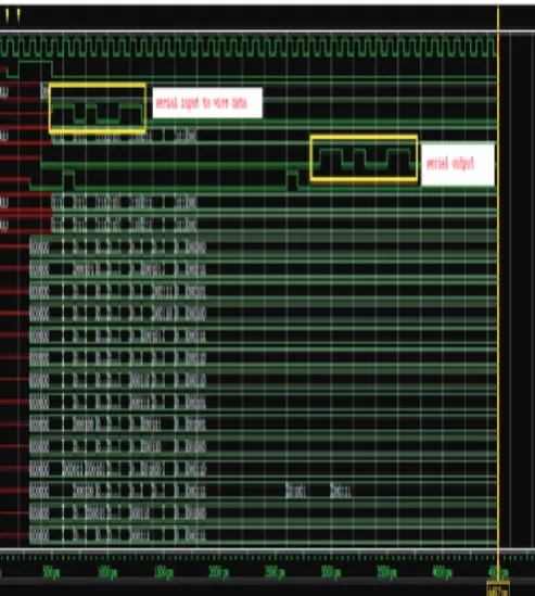
Fig. 3: Simulation Output 1 for MIMO Decoder
Fig. 4: Simulation Output 2 for MIMO Decoder
I. CADENCE
Cadence Design Systems provide global electronic design innovation and plays an essential role in the creation of today’s
electronics.
Elaborate •
Synthesize -to generic •
Synthesize -to mapped •
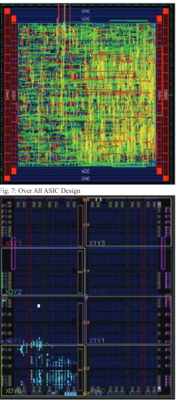
Fig. 5: Design Layout
Fig. 7: Over All ASIC Design
Fig. 8: Synthesis & Implementation Xilinx PlanAhead Output
Encounter(R) RTL to GDSII system Our MIMO decoder gate level model comprised or fitted in Spartan 6 FPGA core this much only. The outer layer is known as SPARATON 6 FPGA.
IV. Efficient Charge Recovery Logic (ECRL)
The principle of operating an adiabatic gate is presented for a buffer gate in the Efficient Charge Recovery Logic (ECRL). The gate consists of two cross-coupled PMOS devices that are used
to store the information. The logic function is construct through
two NMOS device. Input signal for the ECRL gate are shift by 90° with respect to the applied power clock signal. Input is at logic one and the dual input in is at zero. Now the VGS is zero,
gate voltage of device P1 is equal to supply voltage, The PMOS devices will take care of storing the information while both NMOS devices are disable. Then the power clock is reversed from VDD to 0. While p charge from the output is restored to φ.
V. Conclusion
Thus the ASIC implementation of MIMO decoder accelerator
in 45nm technology is obtained. By using Irreversible logic of
MIMO decoder to design a architecture with low power and
energy efficient techniques. First we synthesis the design of our RTL module (MIMO decoder), using cadence RTL compiler to synthesis the design .Here we use 45nm library module for power minimization for the supply voltage achieved by 0.020watt. The accelerator was fabricated in 45-nm CMOS technology.It also offers the latest capabilities to support advanced 65nm and 45nm
designs.
VI. Future Work
The same process can be implemented by using adiabatic logic
method to reduce the area and power consumption. To further improve the system performance.
References
[1] K. Mohammed, B. Daneshrad,“A MIMO decoder accelerator for next generation wireless communications”, IEEE Trans. Very Large Scale Integrator. (VLSI) Syst., Vol. 18, No. 11, pp. 1544–1555, Nov. 2010.
[2] K. Mohammed, M. I. A. Mohamed, B. Daneshrad,“A parameterized programmable MIMO decoding architecture with a scalable instruction set and compiler”, IEEE Trans. Very Large Scale Integrator. (VLSI) System. Vol. 19, No. 8, pp. 1485–1489, Aug. 2011.
[3] M. Shabany, D. Patel, P. G. Gulak,“A latency low-power QR-decomposition ASIC implementation in 0.13 μm CMOS”, IEEE Trans.Circuits Syst. I, Reg. Papers, Vol. 60, No. 2, pp. 327–340, Feb. 2013.
[4] Mohamed I. A. Mohamed, Karim Mohammed, Babak Daneshrad,“Energy Efficient Programmable MIMO Decoder Accelerator Chip in 65-nm cmos”, IEEE Trans. Very Large scale Scale Integrator. (VLSI) Syst., Vol. 22, No. 7, pp. 1481-1555, July 2014.
[5] A. Burg, M. Borgmann, M. Wenk, M. Zellweger, W. Fichtner, H. Bolcskei,“VLSI implementation of MIMO detection using the sphere decoding algorithm”, IEEE J. Solid-State Circuits, Vol. 40, No. 7, pp. 1566–1577, Jul. 2005.
S.Bharani Kumar received his B.E degree in Electronic Communication Engineering from P.R.Engineering College, Vallam, Thanjavur, Tamilnadu, in 2012 and currently, doing M.E degree in Applied Electronics from A.V.C. College of Engineering, Mannampandal, Mayiladuthurai, Tamilnadu, India.
S.Janani received her M.E degree in
communication systems from SSN
College of Engineering, kalavakkam, Chennai, Tamilnadu, in 2009 and she
is currently working as an Assistant
Professor in Department of Electronics Communication Engineering, A.V.C college of Engineering, Mannam-pandal, Mayiladuthurai, Tamilnadu,