ABSTRACT
STANASKI, ANDREW JOHN. Flip Chip testing with a capacitive coupled probe chip. (Under the direction of Paul D. Franzon.)
Testing integrated circuits that employ an area array of I/O presents unique challenges because the face of the chip is not visible for probing. On chips that use perimeter bond pads the face of the chip is exposed, so signals on the wiring in the top layer metal may be probed while the chip is in operation. This is not possible when the face of the chip is hidden.
This work proposes a way to probe test points on the top layer metal of chips that use area I/O. The method works by attaching the chip to a specially designed probe chip instead of the normal packaging. Metal pads on the top layer of the probe chip correspond to lines on the top layer of the chip being tested. These points form a capacitive coupling between the chips, let-ting the probe chip read the signals at the test points. This leaves the original chip largely unchanged, and allows critical signals to be probed.
The geometry of the test points is examined and evaluated using a field solver for their potential to couple between the chips. A square section of metal roughly 6µm on a side pro-vides 1 fF coupling capacitance, enough for a receiver on the probe to reproduce the signal.
The work continues with the design of a receiver circuit to amplify the small input from the test points. The receiver employs a differential amplifier followed by an inverter to amplify the signal without excessive loading at the input. Simulations of the receiver demonstrate its ability to recreate the signal. Additional simulations measure the performance of the receiver under varying conditions, and explore the operational characteristics.
This work also describes the design of a four issue superscalar microprocessor that was used as a reference for explorations of systems design for multichip modules (MCMs). This work focused on the chip testing aspect of area array I/O chips used in an MCM. Other work investigated partitioning, routing, and other system design issues.
A dissertation submitted to the Graduate Faculty of
North Carolina State University
in partial fulfillment of the
requirements for the Degree of
Doctor of Philosophy
ELECTRICAL ENGINEERING
Raleigh
2003
APPROVED BY:
by
FLIP CHIP TESTING WITH A CAPACITIVE COUPLED PROBE CHIP
DEDICATION
BIOGRAPHY
ACKNOWLEDGEMENTS
I would like to thank Paul for his patience and guidance. It has been quite an adventure since that day I walked into your office to ask about the computer architecture class. It turned out to be one of those ordinary events, on an ordinary day, that, when you look back, was a turning point in your life. Thanks for making it a point to remember.
TABLE OF CONTENTS
List of Figures ...ix
List of Tables ...x
Chapter 1 Introduction ...1
Chapter 2 Microprocessor Testing...5
2.1 Introduction ...5
2.2 Background on test methods ...5
2.2.1 Scan: full, partial, boundary ...6
2.2.2 Built-In Self Test (BIST) ...6
2.2.3 Testing Memories ...7
2.2.4 IDDQ...7
2.2.5 Functional Testing ...8
2.2.6 Delay Fault Testing ...8
2.3 Microprocessor test and debug ...9
2.3.1 Typical structured test employment ...10
2.3.2 Functional testing ...11
2.3.3 IDDQTesting ...12
Chapter 3 Chip Debug ...13
3.1 MCM factors ...13
3.2 Probing ...15
3.3 Probing for flip-chips ...15
3.3.1 Optical probing ...15
3.3.2 Capacitive probing ...16
Chapter 4 Capacitive Probe Chip ...19
4.1 Capacitive coupling for digital signals ...19
4.2 The mechanical connection ...20
4.3 The coupling and parasitic capacitance ...21
4.4 The receiver ...27
4.4.1 Circuit description ...27
4.4.2 Receiver performance ...31
4.4.2.1 Nominal performance ...32
4.4.2.2 Effect of process variation ...33
4.4.2.3 Effect of coupling capacitance variation ...35
4.4.2.4 Effect of parasitic capacitance variation ...37
4.4.2.6 High speed performance ...40
4.4.2.7 Edge timing ...41
4.4.2.8 Effect of load variation and crosstalk ...42
Chapter 5 Conclusions and Future Work ...49
5.1 Conclusions ...49
5.1.1 Circuit loading ...49
5.1.2 Timing accuracy ...50
5.1.3 Test setup ...51
5.1.4 Summary ...51
5.2 Future work ...52
Chapter 6 References ...53
6.1 Books ...53
6.1.1 MCM Design ...53
6.1.2 Computer Architecture ...53
6.1.3 Miscellaneous ...53
6.2 Unpublished Papers ...54
6.3 Published Papers ...54
6.3.1 System Testing Case Studies ...54
6.3.2 Chip Testing—Known Good Die ...55
6.3.3 Probes for Bare Chip Test ...56
6.3.4 Capacitive Coupling ...57
6.3.5 Test Cost Analysis ...57
6.3.6 Scan Testing ...57
6.3.7 IDDQ Testing ...57
6.3.8 Delay Testing ...58
6.3.9 Pin Electronics ...59
6.3.10 Test Synthesis ...59
6.3.11 Computer Architecture ...59
6.3.12 Miscellaneous ...60
6.3.13 Chemical-Mechanical Planarization (CMP) ...60
6.3.14 NCSU Papers ...61
Appendix 1 Additional Data ...63
A1.1 Net loading with min sized P transistors, crosstalk ...63
A1.2 Net loading with min sized P transistors, no crosstalk ...65
A1.4 Net loading with up sized P transistors, no crosstalk ...69
Appendix 2 SAND - A Four Issue MIPSµp ...71
A2.1 Purpose of the Project ...71
A2.2 Design Overview ...71
A2.3 Constraints ...72
A2.4 Normal Data Flow ...73
A2.4.1 Fetch ...73
A2.4.2 Decode ...74
A2.4.3 Issue 1—Resolve ...74
A2.4.4 Issue 2—Lookup ...75
A2.4.5 Execute ...75
A2.4.6 Write Back ...76
A2.4.7 Retire ...77
A2.4.8 Resource Sizing ...78
A2.4.8.1 32 Bit Data Path ...78
A2.4.8.2 Instruction Issue ...78
A2.4.8.3 Saving Resources with R0 and Next Cycle Operand ...78
A2.4.8.4 Result Collection ...79
A2.5 Branches and Exceptions ...79
A2.5.1 Branches ...79
A2.5.2 Exceptions ...81
A2.6 Memory Management ...82
A2.7 Coping with Pipelining in MIPS ...83
A2.7.1 Special Registers ...84
A2.7.2 Processor State Changes ...84
A2.8 Implementation ...84
A2.9 Conclusion ...86
Appendix 3 The NCSU Cadence Design Kit ...87
A3.1 Purpose of the Project ...87
A3.2 Functionality ...87
A3.2.1 Design Framework ...87
A3.2.2 Composer (schematic entry) ...88
A3.2.3 Analog Artist (circuit simulation) ...89
A3.2.4 Verilog (digital simulation) ...89
A3.2.5.1 Mask Layers ...89
A3.2.5.2 Parameterized Cells ...90
A3.2.6 Diva (layout verification) ...91
A3.2.6.1 DRC ...91
A3.2.6.2 Extraction ...91
A3.2.6.3 LVS ...91
A3.2.7 Other Functionality ...91
LIST OF FIGURES
Figure 1.1 Speed sorting bare chips ...2
Figure 3.1 Conventional vs capacitive probing ...16
Figure 3.2 Probe chip coupled to the chip under test. ...17
Figure 3.3 Probe electrical schematic. ...18
Figure 4.1 Coupled conductors over substrate ...22
Figure 4.2 Coupled conductors with a crosstalk conductor ...23
Figure 4.3 Coupled conductors having a plate structure ...24
Figure 4.4 Single-ended differential receiver ...28
Figure 4.5 Functional equivalence of one transistor in the linear mode and two transistors in saturation ...29
Figure 4.6 The complete receiver circuit ...30
Figure 4.7 Receiver test bench ...32
Figure 4.8 Nominal receiver performance ...33
Figure 4.9 Receiver response, slow corner ...34
Figure 4.10 Receiver response, fast corner ...35
Figure 4.11 Effect of varying coupling capacitance, all nodes ...36
Figure 4.12 Varying coupling capacitance, circuit output vs. probe output ...37
Figure 4.13 Varying parasitic capacitance, circuit output vs. probe output ...38
Figure 4.14 Output decay ...39
Figure 4.15 High speed operation ...40
Figure 4.16 Output response for varying input periods ...41
Figure 4.17 Circuit under varying load capacitance ...44
Figure 4.18 comp net signal under varying load. ...45
Figure 4.19 Rising edge circuit vs probe edge time difference ...46
Figure 4.20 Falling edge circuit vs probe edge time difference ...47
Figure 4.21 Normalized rising edge circuit vs probe edge time difference ...48
Figure 4.22 Normalized falling edge circuit vs probe edge time difference ...48
Figure A2.1 Normal Data Flow ... 73
Figure A2.2 Result bus timing for a 3 cycle unit ... 76
Figure A2.3 Result forwarding. ... 77
Figure A2.4 Branch unit block diagram. ... 80
LIST OF TABLES
Table 4.1 Probe capacitance for long thin conductors ...23
Table 4.2 Probe capacitance for rectangular conductors...25
Table 4.3 Breakdown of the parasitic capacitance ...25
Table 4.4 Parasitic capacitance of the chip under test in air...26
Table 4.5 Receiver transistor sizing ...31
Table 4.6 Edge difference for varying input periods ...42
Table 4.7 Edge difference for varying load capacitance ...44
Table A1.1 ‘In’ node, min P, crosstalk ...63
Table A1.2 ‘Out’ node, min P, crosstalk ...64
Table A1.3 ‘Ckt’ node, min P, crosstalk...64
Table A1.4 ‘In’ node, min P, no crosstalk ...65
Table A1.5 ‘Out’ node, min P, no crosstalk ...65
Table A1.6 ‘Ckt’ node, min P, no crosstalk...66
Table A1.7 ‘In’ node, larger P, crosstalk ...67
Table A1.8 ‘Out’ node, larger P, crosstalk...67
Table A1.9 ‘Ckt’ node, larger P, crosstalk ...68
Table A1.10 ‘In’ node, larger P, no crosstalk ...69
Table A1.11 ‘Out’ node, larger P, no crosstalk...69
Chapter 1
Introduction
An electronic system implemented on a multichip module (MCM) creates unique and chal-lenging test requirements. An MCM looks like a printed circuit board in miniature, but it takes bare die instead of packaged parts. Therefore, the chips must be tested as a bare die before being integrated on the MCM. Because the thoroughness of the testing has a dramatic impact on the quality of the MCM, the testing must be sufficient to deliver a high percentage of known good parts—a high chip yield.
For an MCM the yield of the module is the product of the individual chip yields.
yieldMCM = yieldchip1 X yieldchip2 X yieldchip3 ... (1.1) If each chip has the same yield, the equation simplifies to:
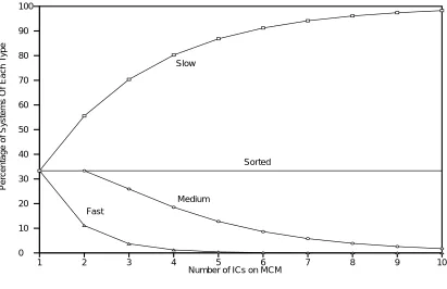
yieldMCM = yieldchipNumberOfChips (1.2) Clearly, more chips and lower chip yields dramatically lower the module yield. For exam-ple, a module with four chips, each with a yield of 90 percent, creates good MCMs at a rate of just 65 percent. Clearly, known good chips are vital to good first pass MCMs. Even with high yield chips, MCM test and rework may be required.
Another chip metric vital to MCM performance is individual chip speed. Chips are often tested to find their maximum operating speed, and binned into speed ratings. Microprocessors are sold by their model and speed rating. The speed rating of a multichip module is deter-mined by the speed ratings of its constituent chips. In general, the module speed rating will be set by the slowest chip, much like the load of a chain is determined by its weakest link.
One aspect of testing the chips is to make sure there are no implementation problems that cause the chip to run slower than expected. The so called timing debug examines chips early in the fabrication run to ensure they meet timing design specs. Sometimes the timing margin on certain paths, critical paths, is too small, and cause the whole chip to run slowly. If the tim-ing modeltim-ing done durtim-ing design was not adequate, the timtim-ing problems will not be detected until after early fabrication runs.
With conventional chips that use a pad ring and wire bonding to the package the face of the chip is exposed and may be probed. For timing debug an electron beam is used to detect sig-nals on top level wiring while the chip is in operation. Analysis of these sigsig-nals may lead the chip designers to the portion of the design causing the timing fault.
With chips employing an area array I/O such probing is not possible. The chip face contains the array of I/O pads. For the chip to operate the I/O points must be connected to power and signals from the test fixture. In doing so the face is covered.
1 2 3 4 5 6 7 8 9 10
Number of ICs on MCM 0
10 20 30 40 50 60 70 80 90 100
P
ercentage of Systems Of Each T
ype
Slow
Medium Fast
Sorted
This work examines a method that allows chips using area array I/O to be operated and probed. The method employes a special probe chip that attaches to the I/O of the chip being tested to provide power and signals to the chip under test. The probe uses capacitive coupling to examine signals on the top layers of the chip under test. The method works with minute levels of capacitance to couple signals to an amplifier on the probe chip. The output of the amplifier gives the design team a glimpse into the working of the chip under test.
The work was undertaken as part of a larger effort to optimize system implementation on multichip modules. Areas of research include partitioning, placement, routing, performance and testing of systems on MCMs.
The rest of this work is divided into the following sections. Chapter 2 surveys a variety of techniques used in microprocessor testing. Microprocessors were used as the system of choice because they employ a wide variety of circuitry, such as random logic and memory. They typi-cally push the limits on clock speeds and have tight timing margins, so they represent the toughest challenges for testing. They also employ a wide variety of testability techniques. Therefore, microprocessor testability design provides a representative study.
Chapter 3 follows with a closer look at the capacitive probing method. It explains in more detail how the concept works. Following that, Chapter 4 dives into the minute detail of the method. It details the mechanical hookup, electrical modeling, probe circuit design, and probe circuit operation. This is the main part of the dissertation.
Chapter 5 presents the conclusions and outlines future work. Following that is the bibliog-raphy and appendices.
Appendix 1 contains extra, detailed data supporting the design of the probe chip.
Appendix 2 describes the design of a four issue superscalar microprocessor created as a ref-erence for MCM design optimization. The Electronics Research Lab (ERL) at N.C. State Uni-versity is examining many aspects of design implementation on MCMs. These efforts include research on system partitioning and routing as well as chip testing. The microprocessor design described was the base used to focus the MCM research work, and provided a sanity check for ideas during the research.
Chapter 2
Microprocessor Testing
2.1
Introduction
Microprocessor design creates the ultimate challenge for silicon test and debug methods. The newest processors continually push the limits of silicon area, speed, and complexity. This makes design for economical test increasingly more difficult, and compensating for the fabri-cation variability all the more critical.
The goal of testing ICs is to verify the design, overcome the large variability inherent in the fabrication process, and ensure proper operation during service. It is currently impossible to produce chips, especially large microprocessors, with near 100 percent yields. Instead each chip must be inspected and tested to prove it operates correctly. In many industries the qual-ity control process provides a manufacturing environment stable enough to make testing fin-ished parts unnecessary. Chip manufacturing is not controllable enough, however, making this quality through inspection process is necessary, though costly. Furthermore, testing can-not adequately validate complex chips without the addition of specific circuitry to enhance a chip’s testability. Thus, there is always a balance between the cost of adding design-for-test circuitry and its impact normal circuit performance, and the amount of test time it takes to achieve adequate fault coverage. There are a number of testing methods that are typically employed and most companies use a similar mix of these methods.
2.2
Background on test methods
2.2.1
Scan: full, partial, boundary
Inserting scan testing involves replacing the normal flip flops in a design with ones having two different inputs. One input is used for the normal function of the flip flop while the other is used to tie the flip flops together, output of one to input of another, in a long chain. Thus, in the test mode, the internal state of the device can be set and read for all the flip flops in the scan chain. This greatly increases the observability and the controllability, and hence the test-ability of the design.
If a design has all of its flip flops connected by a scan chain it is said to be a full scan design. Full scan need not be one single chain. It may involve multiple scan chains, as long as all the flip flops belong to some chain. If some of the flip flops belong to chains and some do not the chip is a partial scan design. One particular type of partial scan that is widely employed is called boundary scan.
With boundary scan the inputs and outputs of a chip contain scan flip flops. These ele-ments can separate the chip from the normal outside signals, giving it isolation from the rest of the system during testing. This is a very useful and popular employment of scan, one that has been standardized as IEEE 1149.1.
As with all hardware insertion for test, scan adds costs to a chip. For scan those costs come from the added area needed to transform the normal flip flops into scan flip flops. The trans-formation can also slow the flip flop speed. The area penalty is unavoidable, but the speed increase can often be accommodated. Only those registers which lie on critical paths, those that set the clock period, are of concern. The speed penalty of a well designed scan cell are a fraction on a nanosecond. In the Motorola 68060 their cell design setup time was less than 0.2ns slower. This small increase is often acceptable to gain the increase in testability.
2.2.2
Built-In Self Test (BIST)
An alternative to using an external tester to generate vectors to stimulate the chip logic, and then read and evaluate the results, is to build on-chip circuitry for those purposes. This is called built-in self test, or BIST. It is often used on specific blocks of a chip.
evaluation circuit often uses a data compression unit, again usually an LFSR, before compar-ing the circuit output to the known good output for that test sequence. Because the pattern generation is done algorithmically BIST is best employed on circuits where algorithmic tests provide good fault coverage. Circuits with regular patterns, like memories, are good candi-dates.
BIST allows the test to proceed at the full clock speed of the chip, without connection to an external tester. As such it can be used while the chip is in service. It can also be buried deep in a chip where access may be difficult. Of course the cost is all the added circuitry for pattern generation and response compaction and memory to store the responses.
2.2.3
Testing Memories
The memory hierarchy of a processor has a profound impact on the overall speed of the sys-tem. Fast CPUs with wide instruction widths demand high bandwidth from the caches to keep them fed. Otherwise the CPI will drop while waiting on the memory. Because memory has such a large impact on speed, processors devote an increasing fraction of the total transistors to memory.
But in order to make the memory fast as well as large it must be carefully designed and tightly packed. Adding any extra circuitry incurs too much area and speed penalty. Therefore, memories are nearly always tested as a block with an external stimulus and response evalua-tion. Fortunately algorithmic tests work reasonably well, so BIST is often effectively used for testing these blocks.
2.2.4
I
DDQMany fault models assume a go-nogo failure pattern in the circuitry. The stuck-at fault is such a model. Many test techniques employ these a models to generate test vectors and deter-mine fault coverage. With CMOS, however, there are other failure modes. For example, typical CMOS failures include gate oxide shorts, and resistive bridges or resistive opens. Go-nogo tests may not detect these problems.
power supply current when there is no switching activity may detect these faults. In fact, this may be the only way to test for some of these faults.
In practice, testing IDDQis not a simple and straight forward task. All real devices have some leakage so setting the “bad” current threshold is a statistical process and is different for each design and fabrication technology. In addition, the logic must be put in a state where these faults lie along a path from the power supply to ground. Determining these vectors and their associated fault coverage in a large chip is not easy. Furthermore, the chip must remain in the quiet state for a relatively long period of time to get an accurate current measurement. This time can be excessive in production when testing a large number of chips.
2.2.5
Functional Testing
Ideally a chip would be partitioned for test into a large number of small clusters of transis-tors with each cluster easily, completely, and independently tested. Realistically a chip is divided into a much smaller number of larger blocks and each block is tested to ensure it per-forms the correct operation. This sort of testing is called functional testing. Often the test uses a fault model, such as the stuck-at model, together with the structure of the circuit to deter-mine the input vectors needed and the fault coverage achieved.
However, some tests may not use a fault model for the circuitry. A test without a model generally uses an ad-hoc procedure to exercise the functionality of the block. For example, a memory block can be written a certain set of patterns, say all ones then all zeros followed by an alternating pattern. Another test might use a pseudo-exhaustive pattern of the inputs to test a large number of input combinations. Or, finally, the test might use a data storage model to determine the sequence of patterns to test that memory. All these examples attempt to ver-ify the correct operation of the block without using the full structural design of the block.
2.2.6
Delay Fault Testing
delay fault testing often goes beyond simply deciding if a chip operates at speed or not. It also attempts to ensure a delay fault can be isolated, robustly tested and the fault location diag-nosed.
Delay fault testing uses two basic models for the cause of excessive circuit delay, the gate delay fault and the path delay fault. The gate delay model presumes the transition time of a gate causes the fault. This model looks a lot like the stuck at fault model with the correct behavior at slower speeds and faulty behavior at faster speeds. However, the accuracy of this model is not great since it assumes all the excess delay is concentrated in one gate.
The path delay model postulates that the extra delay lies along a path to the affected point. This path includes the delays of all the gates in the path as well as the nets. Thus, many pieces contribute to the overall delay time, which reflects the actual condition much more accurately. The difficulty in testing for these delayed paths is in stimulating a single path through a circuit. In order to make a path testable independent of any side path delays, also known as robustly testable, the reconvergent fanout and feedback paths must be cut. A large part of the overhead in delay fault testing goes toward ensuring the proper conditions for path setup. This can be significant.
Because of the cost of making a design delay fault testable, chips using perimeter bonding pads often employ a scanning electron microscope to probe the top layer metal of the chip in a process called voltage contrast (E-beam) testing. The E-beam probe scans a net of interest to determine the waveform on the net. This gives the timing on the net. E-beam testing, how-ever, is not possible on flip-chip die.
2.3
Microprocessor test and debug
improve-ments through reduced CPI than through raw clock speed. But the addition of vast quantity of transistors gained in the new technologies arranged in complex architectures has made chip testing and debug very difficult. Most designers have solved this problem in similar ways.
2.3.1
Typical structured test employment
As chips have become smaller and more complex the number of devices on-chip has grown much faster than the number of inputs and outputs (I/O). Thus, the transistor to I/O ratio has soared which means the controllability and observability of much of the logic has decreased significantly, making it very difficult to test. To access the internal logic most processors employ scan chains. For example, the UltraSPARC™-I has approximately 22,000 scannable flip-flops that give full scan to all logic blocks in the processor except one, which has partial scan [20]. In fact, the PowerPC 603™, Motorola MC68060, and HP PA7100LC all use scan as a primary means of achieving high test coverage [19, 25, 27]. Scan chains provide high con-trollability and observability, and are easy to implement in a design. This keeps the time to market impact to a minimum. However, they cost chip area to make the flip flops scannable, they add a small amount of delay to each flip flop, and the test time increases as the number of flip flops increases. Nevertheless, this technique is adequate for a large group of micropro-cessors.
In addition to an internal scan capability, all processors include IEEE 1149.1 boundary scan with its associated test access port (TAP) controller. System manufactures demand chips contain boundary scan since it makes board testing much easier. And indeed boundary scan has become ubiquitous. Most of the internal testability features, however, do not need the boundary scan features or control.
The expense of BIST led the designers of the 68060 and SPARC processors to a different solution [20–22, 27]. They multiplex the input and output (I/O) pins on the package and acti-vate a special test mode to bring the memory lines to the I/O pins. This makes the chip look like a memory only chip which can be tested directly.
Thus, the structured test methodology found on many processors uses scan chains to test the random logic, either BIST or I/O pin multiplexing to test some of the memories, and func-tional vectors to test any remaining blocks.
2.3.2
Functional testing
The Digital Equipment Corp. (DEC) and Intel use a different strategy for test. They do not use scan chains but rely on progressive functional testing [24, 28]. They start by testing a key memory with BIST. Then the good memory feeds functional vectors to other parts of the chip gradually branching out increasing the verified area. To increase observability they use paral-lel-in serial-out registers that monitor key internal nets.
For Intel this test methodology has evolved through their line of X86 processors. They employ added BIST hardware to exhaustively test the programmable logic arrays (PLAs) and microcode Control ROM. The PLAs and microcode ROM then drive the test on the rest of the chip, including the other memories and the logic.
The DEC approach is similar except they start with the instruction cache. BIST hardware tests the instruction cache which then branches out testing key parts of the logic until other memories in the processors can be checked. Once enough key memories are verified, testing proceeds on the bulk of the logic.
too much area and performance penalty, and would be difficult to design. Widespread use of BIST was far too costly, so they settled on this functional testing plan.
2.3.3
I
DDQTestingThe primary testing methods then divide the chips into the two camps detailed above. I’ll call these the structured approach and the functional approach. This is not the end of the story, however. The UltraSPARC™-I, PowerPC™ 603 and PA7100LC designers also planned their chips to allow IDDQ testing.
IDDQtesting is an excellent method of checking for CMOS faults that do not model well as the usual go-no go (stuck at) type of fault. It is easiest to set up when used with the structured approach because the scan chains permit the state of the machine to be more easily set to a quiet mode. And indeed the chips using IDDQ are all from the structured camp. The results from using IDDQtesting can be a dramatic drop in the failure rate during functional testing. Reference [52] gives some typical results.
Chapter 3
Chip Debug
The testability features detailed in the previous chapter are all generally targeted toward checkout of chips during volume manufacturing. During the design cycle those features must also support debug. The scan chains of the structured approach lend themselves to this task. Scan breaks the logic into many smaller blocks which helps pinpoint the location of faults. In other words, it gives high observability and controllability. The various SPARC chips have a planned methodology utilizing the full scan built into them to provide detailed debug informa-tion [20, 21, 23]. This includes control of the clock driver, use of the scan chains, and modes to dump the contents of the internal memories.
The functional approach requires more effort. It uses observability registers placed at key points to see small, critical pieces of the design. Intel call this the scanout methodology [28]. Choosing the optimum placement of these observation blocks for maximum benefit at the low-est cost takes considerable effort. Special ports that bring critical nets out to pins, or allow the memories to be read, supplement the observation blocks. This sort of design effort makes sense for a high volume producers, like Intel, who want to minimize the test circuitry per chip, and for those who want to run the clock as fast as possible.
3.1
MCM factors
On an MCM the electrical cost of interconnect is less than in a single chip package. The MCM substrate provides a high line count interconnect with lower parasitic factors than a conventional printed wiring board (PWB). This can lead to a different circuit partitioning than single chips on PWB. Chips may have many more I/O, and because off-chip signals are not as electrically costly, the system designer may choose to place circuit elements requiring high interconnect on different chips. One obvious partitioning is to separate most of the cache memory from the logic. As long as the memory hierarchy can sustain the processing rate of the logic the partitioning will be effective [11]. Bare die with area array I/O used on an MCM support such a partitioning.
This provides an opportunity and a dilemma for testing. Traditional VLSI testers are not geared toward running bare chips with huge I/O counts, and the smaller drivers may not be adequate to drive the tester. There are techniques that can solve this problem. To test the bare die a membrane probe is often used. Membrane probes started as a high quality probe for testing at the wafer level [41, 42]. Because they have the unique combination of small feature size that allows high bump density, and good parasitic qualities, they became a natural choice for probing bare die with area array I/O [43–47]. The latest technologies resemble the MCMs they are emulating, and the probes have shown they can operate thousands of I/O at frequen-cies beyond 1 GHz [44]. This allows normal production testing of bare die.
Another method uses an interposer. Connection to an interposer creates a single packaged part, also called a chip scale package [87]. This may be testable in a VLSI tester.
In combination with a membrane probe or interposer, the VLSI tester can be expanded by using a smart test head. The smart test head incorporates drivers, both to and from the tester, as well as design for test features, such as pattern generation, signal compaction and analysis, and IDDQ for the power supply lines.
A smart test head provides significant benefits. The test head can be programmed to per-form some of the chip testing autonomously. This reduces the memory requirement of the VLSI tester. It may also allow one VLSI tester to drive more than one test head at the same time. In addition, placing the IDDQmeasurement close to the chip provides for high quality measurement.Each power entry point can be measured individually.
There is a cost in building a smart test head. The head circuitry must operate at least as fast as the chip under test. In addition, the head design must be general enough to be used on several different chips to keep the cost reasonable. Generalized circuitry means any I/O can be treated as either a signal or power pin. Thus, the head must be configurable to connect power and ground to the appropriate pins, and measure IDDQon those, if desired. The head must be able to drive the signal I/O with appropriate patterns and to observe the results. If testability is used, the head must be able to decide on the correctness of the results.
These methods provide for normal production testing. But what about pre-production debug of chips to resolve design flaws, such as timing problems?
3.2
Probing
Adding circuitry to the chip for test, costs area, design time, and complexity. The goal is to add the minimum amount of overhead that provides adequate coverage. But even with the added test circuitry that provides sufficient coverage for production checkout the engineers may not be able to pinpoint the location all of the chip faults during debug. When this hap-pens they turn to probing. With a voltage contrast (E-beam) probe they can observe many more signals and determine their timing. While this has been successful in many cases, the method has limits. It can only read the top layer metal, and it can only run on chips with access to that metal while the chip is running. Newer fabrication processes continue to add more metal layers which limits the visibility of many signals to the E-beam probe. It may be necessary to bring critical signals to the top layer expressly for probing. More importantly, this sort of probing requires the top of the chip be visible while in operation which limits it to chips with perimeter bonding pads. New designs utilizing an area array I/O across the entire chip are mounted face down which will foil the E-beam technique.
3.3
Probing for flip-chips
For debuging chips with area array I/O, a manufacture will either have to employ more test logic on chip, or use another technique for probing. Here are some other ideas for probing.
3.3.1
Optical probing
when the output is charging or discharging and the crowbar current flows. You can, essen-tially, see the signals propagating through a chip. It was not clear from the literature, how-ever, the optical resolution available. Can it resolve the emissions from individual transistors on a large deep submicron chip? It would have to have this capability to be useful.
3.3.2
Capacitive probing
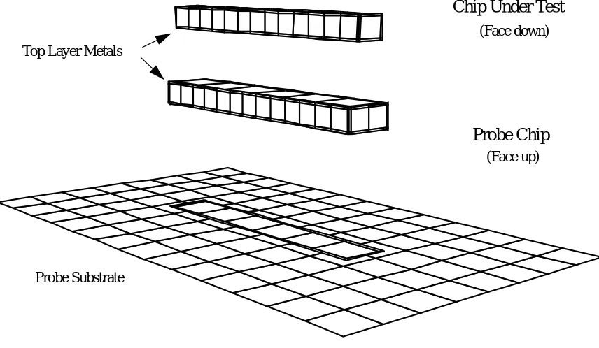
The approach we investigated uses capactitve coupling to probe the chip to determine the signal timing. The idea is to use a very small capactitve probe to view the signal lines on the top metal layer of the chip you want to debug. The probe is actually a chip itself that acts as a carrier for the device under test and probes selected signals by coupling between the top layer metal on each chip. This is shown in Figure 3.1.
The probe chip holds the chip under test, distributes the normal input signals to it, and probes the signals of interest. To maximize the coupling capacitance of the signal probe oper-ating between the two chips their faces must be as close as possible. To reduce the gap, ideally to nothing, the solder bumps on the chip under test must be reduced to a very small size. We call these micro-bumps. This is not a big design change for the chip, only the overglass cut needs to change to reduce the exposed pad area and form a small solder ball. A corresponding hole is etched into the probe chip to accommodate the bump. During normal production the
Flip-Chip Capacitive Probing
Conventional Perimeter Bond Chip Probing
Probe Chip Chip Under Test
Chip Under Test E-Beam Probe
Package
Package
overglass cut mask produces the regular opening for standard size solder balls. A close in view of the two chips together is shown in Figure 3.2.
Micro-Bump
Probe Chip
Chip Under Test
.Electrically the two chips form a circuit like that in Figure 3.3. The top metal layers on the
chips forms a capacitor which couples the signals passing through the chip under test onto the probe chip. These signals on the probe chip are then amplified and passed to the edge of the chip where they can be observed.
Chapter 4
Capacitive Probe Chip
There are a number of design issues to consider in the probe chip. First, it has to mechani-cally support the chip under test and pass to it the normal signals. This involves constructing small solder balls on the chip under test and having a receptor site on the probe chip that mates to these balls such that the chip faces stay very close together. At the same time, the solder connections must still be electrically sound. Next, the nature of the capacitive coupling must be examined to ensure a viable signal path can be made between the two chips. Finally, a suitable receiver has to be constructed to regenerate the signal induced in the probe chip. This chapter explores these issues after a look at some previous uses of capacitive coupling for digital signals.
4.1
Capacitive coupling for digital signals
There have been some attempts to demonstrate capacitive coupling as a means of passing digital signals. Reference [50] argues for using capacitive coupling for all chip I/O signaling. In this scheme the normal conductive I/O array is replaced with plates in the top layer metal that form capacitors with the underlying substrate, which is assumed to be a multichip mod-ule (MCM). The signaling is then done with pulses that can pass through the capacitors. They suggest a value of about 1 pF for each pad. In their discussion of the electrical characteristics they state that this arrangement will have “substantially zero parasitics.” However, they have ignored the capacitance the I/O plate has with the chip substrate or wiring beneath the plate. This parasitic capacitance is substantial, on the same order as the coupling capacitance. In fact the entire discussion forms a high level argument for capacitive coupled signaling with little detailed analysis of any specific cases.
uses feedback to prevent the signal decay or “zero wander” of the coupled signal and holds the digital signal at the correct levels. The design is useful for connecting chips that use different DC voltage levels for bit representation since the DC component does not pass through the capacitor. But it requires differential signaling and uses a total of 3.2 pF capacitance per sig-nal pair. The probe chip only has single ended sigsig-nals available and a capacitance value that is orders of magnitude smaller than either of these approaches.
4.2
The mechanical connection
The first problem is to connect the chip under test to the probe chip and keep their faces as close together as possible, ideally touching. This was depicted previously in Figure 3.2. The chips connect through the usual solder bump interconnections the chip under test will ulti-mately employ for bonding to the MCM substrate. However, to achieve the second require-ment pits must be etched into the probe chip to accept the bumps on the test chip and keep the faces close. If the normal size solder bumps of around 100µm diameter are used then the craters would have to be huge, over 50µm deep. Such large connections are not really neces-sary though, since they do not have to pass the normal reliability criteria as they will only be used for chip debug and not in normal service. Therefore, smaller bumps, call them micro bumps, of around 20µm diameter can be used. This only requires a depth of something over 10 µm. These holes have insulator grown, a normal signal conductor metal and a wettable metals deposited to form the receptors for the solder bumps. The chip under test only needs smaller overglass cuts to reduce the bump size. The mask changes for the chip under test are, therefore, small.
Another factor in how close the faces of the two chips can get is how flat those faces are manufactured. Most processes use some form of chemical-mechanical planarization (CMP), a.k.a. chemical-mechanical polish, to assure flatness during manufacturing. References [94] and [95] indicate CMP can achieve a high degree of flatness. They report a half micron varia-tion over a three inch wafer.
With the chips flat and pushed as close together as possible one would hope for a perfect match between the chip faces where glass touches glass and there are no gaps. Air, as every-one knows, makes a poor dielectric. Capacitors with air gaps between the plates do not gener-ate a very high value of capacitance. In practical terms it is impossible to have the chip faces perfectly touching. The resulting air gap will ruin the coupling we are trying to achieve between the chips. Thus, it is necessary to fill those gaps with a high dielectric material to promote coupling. A liquid glycol fill, withεr= 80, can do the task. It will wick into the space between the chips and provide a good coupling dielectric.
There are other chip coupling mechanisms beside solder bumps. This work focused solder bumps because they are the most common area array connection technology. There are alter-natives, such as conductive polymers [1] and other technologies, that may be usable. However, these are not widely employed.
4.3
The coupling and parasitic capacitance
To investigate the values of the various coupling and parasitic capacitances in the circuit formed by the joined chips I used the fastcap field solver to simulate different stacks of con-ductors and dielectric. These stacks represent a cross section of the two joined chips. The fab-rication process chosen has a 0.35µm effective feature size and the conductor and dielectric thicknesses and spacings were taken from the process manual. The process was assumed to be planarized so the tops of all the dielectrics, except the overglass, were treated as flat planes. The overglass was made conformal over the top layer metal. Also, the simulation assumed the top of the substrate is a perfect conductor. In reality it is not a perfect conductor which would increase the effective distance to this plate when used as a capacitor, lowering the capacitance. Therefore, because coupling to the substrate creates a parasitic capacitance, this simplification presents the worst case.
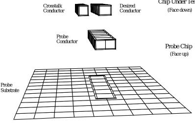
set-ting out to make an intentional coupling capacitor this is a problem. Figure 4.1 shows a
depic-tion of a probe chip and a chip under test using normal thin metal lines for coupling. The dielectric interfaces were removed for clarity. The chip faces were assumed to not touch. Instead a gap of 1 or 2µm was used. The metal on the probe chip was made 1µm wider than the metal on the chip under test to increase the coupling and accommodate misalignment. This case requires a length of around 14µm to achieve a 1 fF coupling value. And, as shown in Table 4.1, this geometry gives a large parasitic capacitance, resulting in a poor coupled to par-asitic ratio. Furthermore, in the presence of a second conductor on the chip under test, paral-lel to the one of interest, the probe metal will pick up a large crosstalk component from this
Figure 4.1 Coupled conductors over substrate
Probe Chip
Chip Under Test
Probe Substrate Top Layer Metals
second conductor. This is depicted in Figure 4.2 and also shown in Table 4.1. With the large
Table 4.1 Probe capacitance for long thin conductors
Capacitance Type
Chip to Chip Gap
1µm 2µm
No Crosstalk Conductor
Coupling Cap 1.215 1.015
Parasitic Cap to sub-strate
1.013 0.981
Parasitic Cap to other sources
0.895 1.239
Parasitic Cap total 1.918 2.221 Coupling/Parasitic Ratio .633 .457
Figure 4.2 Coupled conductors with a crosstalk conductor
Probe Chip
Chip Under Test
(Face up) (Face down)
Probe
Desired Crosstalk
Conductor Conductor
Probe Conductor
amount of parasitic capacitance relative to the coupled capacitance the signal propagated to the receiver circuit may be too small to be of use. Also, the magnitude of the crosstalk compo-nent may overwhelm the signal.
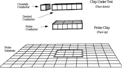
To improve the coupling the conductors must change to a more rectangular geometry. Using a square shape 6.3 µm on a side, as shown in Figure 4.3 with a crosstalk conductor,
With Crosstalk Conductor
Coupling Cap 0.853 0.700
Crosstalk Cap 0.663 0.596
Parasitic Cap 1.628 1.937
Coupling/Parasitic Ratio .523 .361 Capacitance values in fF
Desired conductor 1.5 x 14.1µm Probe conductor 2.5 x 14.1µm
Table 4.1 Probe capacitance for long thin conductors
Capacitance Type
Chip to Chip Gap
1µm 2µm
Figure 4.3 Coupled conductors having a plate structure
Probe Chip
Chip Under Test
(Face up) (Face down)
Desired Crosstalk Conductor
Conductor
Probe Conductor
greatly improves the coupled to parasitic ratio. Table 4.2 shows these results. Now the
cou-pling should be sufficient to provide a useful signal. Also note the crosstalk component remains relatively small.
The parasitic capacitance given in Tables 4.1 and 4.2 includes all the capacitance not cou-pled to either the desired conductor or the crosstalk conductor. Part of this parasitic capaci-tance goes to the substrate and the rest to other stray sources as indicated in Table 4.3. This
stray component increases as the distance between the chips increases because the interven-ing space is filled with the high dielectric strength fluid. As the distance increases somewhat
Table 4.2 Probe capacitance for rectangular conductors
Capacitance Type
Chip to Chip Gap
1µm 2µm
No Crosstalk Conductor
Coupling Cap 1.323 1.095
Parasitic Cap 1.603 1.957
Coupling/Parasitic Ratio .825 .560 With Crosstalk
Conductor
Coupling Cap 1.163 0.954
Crosstalk Cap 0.295 0.272
Parasitic Cap 1.487 1.816
Coupling/Parasitic Ratio .782 .525 Capacitance values in fF
Desired and probe conductors 6.3 x 6.3µm
Table 4.3 Breakdown of the parasitic capacitance
Parasitic Capacitance
Chip to Chip Gap
1µm 2µm
No Crosstalk Conductor
to substrate 0.883 0.848
to other sources 0.719 1.108 With Crosstalk
Conductor
to substrate 0.892 0.872
fewer field lines couple between the probe and the desired conductors, but a greater number of stray field lines in the gap can terminate at the probe conductor or the desired conductor. Thus, a larger gap increases the parasitic capacitance at both the probe conductor and the desired conductor, and both the probe conductor and the desired conductor see a similar effect. The total load on the desired conductor is equal to the normal on-chip load plus the extra load added by the test fixture (probe chip). The normal load consists of the capacitance of the devices attached to the line, which are not indicated in the fastcap simulations, and the usual parasitic capacitance for the line. The load on the desired conductor imparted by the test fix-ture equals the coupling capacitance plus the stray parasitic capacitance. For the coupled sec-tion the stray capacitance is about 1 fF (Table 4.3) and the coupling capacitance is at most about 1.4 fF (Table 4.2). Under normal operation the same section would have air above it and would have a stray capacitance of about 0.6 fF. This is shown in Table 4.4. Therefore, the probe chip adds approximately 1.8 fF to the line load.
However, the coupled section is normally attached to additional wiring. The additional wiring would connect the coupled section to the rest of the chip under test. The load capaci-tance for a length of (thin) conductor that could be used for such a purpose is about 2.2 fF per 14µm of line length (Table 4.1) when used with the probe chip and 0.64 fF when alone. So the probe chip adds about 1.6 fF per 14µm length.
For example, assume a total line length of 34µm consists of two 14µm sections and the 6 µm coupled section. The total additional load presented by the probe chip would be 5.0 fF.
Table 4.4 Parasitic capacitance of the chip under test in air
Parasitic Capacitance Value
4.4
The receiver
4.4.1
Circuit description
gain is not as high as when connected as a true differential pair with current mirror loads, but it has sufficient gain to recover the signal. When deployed with a second stage the full output swing is achieved. Details of the biasing will be discussed in a moment.
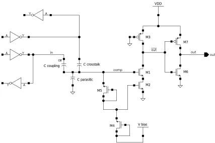
Because of the way the differential pair is used it is possible to collapse the functionality of the reference leg formed by transistors M2 and M3 into a single transistor. In [91] the authors demonstrate a functional equivalence in the current response between a pair of FETs operat-ing in the saturation region to a soperat-ingle FET operatoperat-ing in the linear region. This happens because the drain current of a saturated transistor depends only on the gate voltage, Vgs. The drain-source voltage, Vds, has little impact on the current. Thus, there is only one component to the current, the forward current IF, as determined by the gate voltage.
(4.1)
M1 M2
M3 V bias1
V bias2 R1
R2 C couple
C parasitic
V out Circuit Under Test
VDD
V ref
Figure 4.4 Single-ended differential receiver
Ids
W
L
---
β
2
--- Vgb
(
–
Vsb
–
Vth
)
2I
FIn the linear region both Vgs and Vds impact the drain current. So there are two compo-nents to the current, forward IF and reverse IR.
(4.2) Imagine each of these two components of the drain current, IFand IR, in the linear transis-tor being replaced with an equivalent current generated by a saturated transistransis-tor. Then two transistors in saturation would be functionally equivalent to a single transistor in the linear region, as depicted in Figure 4.5.
Using this equivalence we can replace the two transistors in the reference leg of the differ-ential amplifier operating in the saturation mode with a single transistor in the linear mode.
For biasing we need to replace resistors R1 and R2 with components buildable in MOS. For the load resistor R1 we can use a PMOS transistor biased on. Changing the length and width of the channel sets the resistance. Constructing R2 is more complicated because of the high value needed to minimize the load on the input line. Unfortunately, high value resistors are difficult to build in MOS processes. The solution is to use a pair of diode connected NMOS transistors in series. With these added the complete receiver is shown in Figure 4.6.
Ids
W
L
---
β
2
--- Vgb
[
(
–
Vsb
–
Vth
2)
–
(
Vgb
–
Vdb
–
Vth
)
2]
I
F–
I
R=
=
M1
M2
M3 Ids
IF
IR
Ids
Figure 4.5 Functional equivalence of one transistor in the linear mode and two
The voltage drop across each of the diode connected bias transistors, M4 and M5, is higher than normal due to significant body effect which raises the threshold voltage. These bias tran-sistors allow the receiver input, called “comp” in the schematic, to charge up to the low input voltage, VIL, for the receiver. At that point the transistors reach cutoff giving them a very high resistance. A positive pulse from the coupling capacitor drives the bias network further into cutoff, increasing the resistance further. The gate of M2, which servers as the reference for the differential pair, maintains a higher bias voltage than M1, the signal input. This sets the baseline current through the differential amplifier. The bias and size of the reference transis-tor, M2, and size of the load transistransis-tor, M3, determine the output voltage operating point at net called out bar. The input and reference transistors, M1 and M2, are set at the same size so they share a common diffusion so they will be as closely matched as possible. A second stage
M1
M2 M3
M4 M5
M6 M7
C coupling
C parasitic C crosstalk
V bias VDD
inverter consisting of M6 and M7 restores the output to full voltage swing and completes the receiver. The transistor sizing is shown in Table 4.5.
Using a differential amplifier helps minimize noise interference. Because M1 and M2 are in the same diffusion, substrate noise will likely be common to both. Likewise, noise on M4 will go into both inputs. This common mode noise should have little impact on performance. Only noise into M5 will have a direct impact on the input. Using a separate clean bias supply, and substrate guard rings will minimize noise introduction.
4.4.2
Receiver performance
The receiver performance was determined using HSpice from within the Cadence Analog Artist environment. The transistor models were level 28 with binning obtained from the pro-cess manufacturer. The propro-cess had a 0.4µm drawn minimum feature size. As shown in Fig-ure 4.7, the input signal sources were buffered through a transmission gate selector and two levels of gates before feeding the coupling capacitance network. Also connected to this net, called “in”, are additional capacitors used to vary the loading of the drive circuit and a non-inverting buffer. The output of this buffer, net name “ckt”, served as the golden reference to
Table 4.5 Receiver transistor sizing
Transistor Length Width
M1 0.5 0.8
M2 0.5 0.8
M3 0.7 0.8
M4 0.6 0.8
M5 0.6 0.8
M6 0.4 0.8
M7 0.4 0.8
All lengths in microns.
HP CMOS 10 process, MOSIS SCMOS_SUBM rules. Min Length = 0.4µm
compare to the output of the receiver. In addition, the output from the inverting gate in the input buffer feeds the crosstalk capacitor in the coupling network providing the worst case crosstalk to the receiver.
A number of runs were conducted using parametric analysis to set the transistor sizes. Most of the transistors in the receiver have a gate length longer than minimum to reduce the performance fluctuation due to process variation. This is an analog design technique that makes the receiver stable over a wide range of conditions. Reference [92], particularly Figure 1A, shows the variation of gate length in a similar size fabrication technology.
The capacitance network takes the values from Table 4.2. The nominal value for the cou-pling capacitance was set to 1.2 fF, the parasitic capacitance was set to 1.4 fF, and the crosstalk capacitance was set to 0.275 fF.
4.4.2.1 Nominal performance
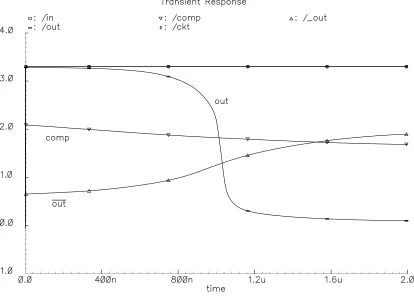
The nominal performance is shown in Figure 4.8. Charge from the signal of interest, “in”, increases the voltage on the receiver input, “comp”, from its resting point set by the bias sup-ply. The effect of the out of phase crosstalk net propagating charge through the crosstalk capacitor shows up as the dip in the rising edge of the comp signal (near the point where the “in” signal crosses the “comp” signal). As the comp voltage rises, current in the differential amplifier rises, dropping the voltage at the output of the amplifier, out bar. This drives the second stage inverter to swing the output from low to high. For the falling transition the input drains charge away from the comp net and the voltage falls. This reduces the current out of
Figure 4.7 Receiver test bench
C crosstalk
C coupling (C0) C parasitic
Input V bias
Sources
V select
the differential pair allowing the pull-up load to increase the voltage at out bar. This, of course, drives the second stage inverter high to low. The voltage gain of the differential ampli-fier is 3.7.
4.4.2.2 Effect of process variation
To investigate the effect of process variation I used the transistor corner models available for this process. The models show the type of variation that may be expected from batch to batch in a chip run. The amount of change indicated in the models is much wider than one would expect within a single chip. Reference [93] shows a distribution of threshold voltages across chips on a wafer. The variation of the voltage on a single chip is much smaller than the
In
Out
Ckt
Comp
Out
In
Out
Ckt
total variation across all chips on the wafer. Thus the models are too wide to apply to an indi-vidual chip.
The simulation runs with the corner models, shown in Figure 4.9 for slow transistors and Figure 4.10 for fast transistors, indicate the receiver operating point changes with the model. By making a small correction to the bias voltage the receiver can be tuned to operate very close to nominal.
Figure 4.9 Receiver response, slow corner
3.5
3.3 3.3 3.5
Receiver Output
4.4.2.3 Effect of coupling capacitance variation
It is also important to understand how the receiver performs if the values of the capacitors in the coupling network vary. For these experiments I varied the capacitance values over the range indicated in Table 4.2. That is, I set the coupling capacitance from 1.0 fF to 1.4 fF, and the parasitic capacitance from 1.4 fF to 2.0 fF. The crosstalk capacitance stayed at 0.275 fF since the fastcap simulations indicate it does not vary a significant amount. Each parameter was varied separately while the others were held at their nominal values, 1.2 fF for the
cou-3.1 3.3
3.1
3.3
Figure 4.10 Receiver response, fast corner
Receiver Output
pling capacitance and 1.4 fF for the parasitic capacitance. The effect of varying the coupling value is shown in Figure 4.11 and Figure 4.12.
As one would expect, the change in the coupling capacitance makes a marked impact on the amount of charge transferred to the comp net. Hence, the voltage range is quite reduced as the capacitance diminishes. The lower voltage at the smallest coupling value presents the most difficult challenge to the receiver. The output is still acceptable, as shown in Figure 4.12, but you can see how the slope of the probe output is affected. It is particularly evident on the rising edge where the out of phase crosstalk signal slows the rising edge of the comp net. It is no surprise that from the receiver’s point of view it is always desirable to have as large a cou-pling capacitor as possible.
Another characteristic to note is that as charge is taken out of the comp net and the voltage approaches the bias point, if the input signal is sufficient to drive the voltage below the bias level the bias transistors will turn on to restore the voltage. This can be seen in Figure 4.11 in the small dip at the end of the falling transition of the comp node. In effect, the bias network will never let the voltage drop below the bias level on the comp net.
4.4.2.4 Effect of parasitic capacitance variation
The effect of varying the parasitic capacitance value is shown in Figure 4.13. As one would expect the parasitic variation has less effect on the circuit performance than the coupling capacitance. In fact, the entire range of parasitic values change the shape of the probe output
very little. This reinforces the notion that a larger coupling capacitance is beneficial, even if it increases the parasitic capacitance, because an increase in parasitic capacitance has little consequence, whereas an increase in the coupling capacitance strongly influences the output.
4.4.2.5 Capacitive charge decay time
As with all capacitive coupled amplifiers the input bias is important. Since the bias net-work in this design employes no feedback, when the comp net is driven to its high input volt-age, VIH, the charge on the node will eventually decay back toward the bias point. In other words, when there is no signal the receiver input (comp) will always move to VIL. This results in two consequences. First, the receiver must transition from low to high (rising transition)
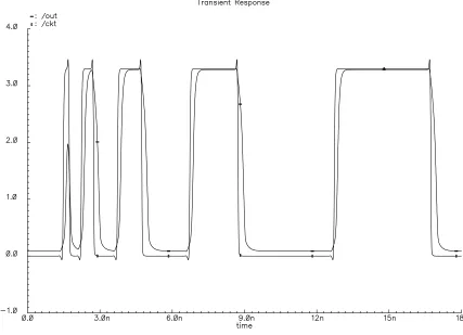
before going from high to low (falling transition). If a falling transition were to happen before a rising transition the comp node would simply be driven to turn on the bias network and the node would be held at VIL. Second, the high to low transition must occur before the signal has decayed to the point of switching the output of the receiver. Eventually the output of the rising transition will decay below the threshold required to keep the output high. Once this happens the edge a falling transition is lost. Figure 4.14 shows the receiver can hold at the high output for about 1µs. For a system running at 100MHz (10ns cycle time), a typical clock rate for this process technology, the test would have 100 cycles to trigger a falling edge. Using a more con-servative 800ns to remove any doubt as to the validity of the cause of the edge the test would still have 80 cycles to trigger a falling edge.
4.4.2.6 High speed performance
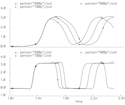
At the other end of the range a designer may be concerned with the maximum rate the receiver can switch. It takes more time to propagate a signal through the coupling capacitor, charge the parasitic capacitor, and change the state of the receiver than just driving an output gate directly. Figure 4.15 shows the output of the probe versus the output of the reference cir-cuit at several periodic input signal rates. The fastest rate shown is 700 ps, which is over 1.4 GHz. This should allow use of the probe with the fastest digital signals generally in use with this process technology.
4.4.2.7 Edge timing
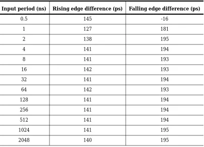
Figure 4.16 shows the response of the circuit and probe output superimposed while the input period varies from 500ps upward. At 500ps the probe cannot respond effectively to the input. Above that, however, the probe and the circuit match well. Ideally the difference in the circuit edge and the probe edge should remain constant regardless of the cycle time of the input signal. Taking the X intercept at the 50 percent crossing, Table 4.6 shows that the mini-mum difference for the rising transition is 127ps and the maximini-mum difference is 141ps. The variation is 14ps. The minimum value occurs at when the input period is 1ns. At 2ns input period and above the variation is only 3ps. The falling transition variation is identical, 14ps when the input is 1ns and 3ps when the input is at or above 2ns. This holds out to a period of 2µs.
4.4.2.8 Effect of load variation and crosstalk
Finally, the response was measured as the load capacitance on the test circuit, the “in” net, varied. The capacitors, Cload in Figure 4.7, act as a variable load, simulating the driver in dif-ferent fanout conditions. Figure 4.17 shows the driver signal, in, and the receivers responses. The load was varied in increments up to the point where the input edge rise and fall times were about an order of magnitude slower than the case with no additional load. The exact change in rise and fall times is 11 to 12 times slower.
As with the previous case the difference in the edge timing between the buffer circuit and the probe circuit was measured at the 50 percent voltage point and summarized in Table 3.6. What stands out is how the edge difference increases as the load increases and the driver edge flattens out. It appears as though the probe triggers at a different point along the input edge than the buffer circuit, causing the difference in timing. This could be explained by the nature of the circuitry. The capacitive coupled probe takes longer to accumulate enough charge to effect the switch in its output stage. However, the actual causes are more complicated.
Table 4.6 Edge difference for varying input periods
Input period (ns) Rising edge difference (ps) Falling edge difference (ps)
0.5 145 -16
1 127 181
2 138 195
4 141 194
8 141 193
16 142 193
32 141 194
64 142 193
128 141 194
256 141 194
512 141 194
1024 141 195
First, part of the reason the rising and falling edges have a dissimilarity in the rate of increase of the delay difference is because the response of the gate driving the “in” net has a different rising response versus falling response. This happens because the transistors in the gate are the same size, and the n-channel device has an inherently greater drive than the p-channel device. The net result is unequal rise and fall times, which is especially pronounced when the load increases.
Table 4.7 Edge difference for varying load capacitance
Load Cap (fF) Rising edge difference (ps) Falling edge difference (ps)
0 141 194
10 168 191
20 190 193
30 209 198
40 227 203
50 244 204
To study these effects I ran simulations with the crosstalk signal present, as just described, and with it absent. I also used a driver gate with equally sized n and p transistors and one where the p-channel device was increased in size to give equal rise and fall times. Plots of the signals at the comp net for the four cases is shown in Figure . The plots on the left
side of the figure include crosstalk, while those on the right do not. On the top the driver had equal size transistors, and on the bottom equal rise and fall times (larger p-channel devices). The simulations with the larger p-channel transistors employed a larger load to give
mately the same pull up response as the smaller driver. Of course, this makes a noticeable change in the falling edge response. Its slope shifts closer to that shown for the rising edge.
The plots in Figure 4.18 show the crosstalk signal does indeed have a pronounced effect in the probe input as the driver load increases. With a small load the fast edge of the driving sig-nal overwhelms any charge from the crosstalk path. The effect of the crosstalk is barely noticeable. As the driver edge slows down the steady crosstalk signal becomes more pro-nounced, and the timing of its effect shifts to earlier in the edge transition. This not only slows down the rise time and fall time of the edge into the probe, it also changes the slope in the crit-ical transition region. This, in turn, changes the probe output timing.
To quantify the timing change I took 50 percent point measurements for each of the four cases at the circuit and probe outputs and computed the time differences of the edges. These differences are summarized in the graphs shown in Figure 4.19 and Figure 4.20. In these fig-ures “MinP” is the case with equal sized transistors, and “Equal” is the case with larger p-channel devices for equal rise and fall times. The extra load is contributed by Cload. Since the n-channel devices do not change size, only the two curves for equal rise and fall times are given because they used a larger loading capacitance range. The minimum p-channel case is just a subset of these.
Figure 4.19 Rising edge circuit vs probe edge time difference
0 10f 20f 30f 40f 50f
0 50 100 150 200 250 300 350 400 450
Delay Difference - Rising Edge
MinP Xtk Rise
MinP No Xtk Rise
Equal Xtk Rise
Equal No Xtk Rise
Ti m e (p s )
30f 60f 90f 120f 150f
Ideally the difference would remain constant regardless of the load and the graphs would show horizontal lines. Obviously, the loading introduces some error in the relative timing of probe. Interestingly, for the rising edge the timing difference actually decreases when there is no crosstalk signal as shown by the down sloping curves. This is not necessarily desired. A flat line with a constant offset would be better. The absolute value of the change from the zero additional load condition is the important parameter.
Figure 4.21 and Figure 4.22 show the same data in a presentation that makes this clear. These figures plot the absolute value of the delay difference change. Here zero represents no change from the zero extra load case. Thus, zero is desired.
The worst case appears in the falling edge transition with no crosstalk. This is the top curve in Figure 4.20 and Figure 4.22. It shows a 200ps difference from zero to maximum load. The next worse cases indicate just over 100ps difference. These are rising edges with crosstalk.
Figure 4.20 Falling edge circuit vs probe edge time difference
0 30f 60f 90f 120f 150f
0 50 100 150 200 250 300 350 400 450
Delay Difference - Falling Edge
Equal Xtk Fall
Equal No Xtk Fall
T
ime
(p
s
)
Figure 4.21 Normalized rising edge circuit vs probe edge time difference
0 10f 20f 30f 40f 50f
0 25 50 75 100 125 150 175 200
Delay Difference Change - Rising Edge
MinP Xtk Rise MinP No Xtk Rise Equal Xtk Rise Equal No Xtk Rise
Load (fF) T ime (p s ) Extra
30f 60f 90f 120f 150f
Figure 4.22 Normalized falling edge circuit vs probe edge time difference
0 30f 60f 90f 120f 150f
0 25 50 75 100 125 150 175 200
Delay Difference Change - Falling Edge
Equal Xtk Fall Equal No Xtk Fall