ISSN (Print) : 2320 – 3765 ISSN (Online): 2278 – 8875
I
nternational
J
ournal of
A
dvanced
R
esearch in
E
lectrical,
E
lectronics and
I
nstrumentation
E
ngineering
(An UGC Approved Journal)
Website: www.ijareeie.com
Vol. 6, Issue 8, August 2017
Power Factor Corrector Boost Converter with
Self Tuned PID Controller by Genetic
Algorithm
G.Sarojini Devi, Dr. A.Lashmi Devi
M.E, Dept. of EEE, SKIT Sri Kalahasthi, AP, India Professor, Dept. of EEE, S.V.U. College of Engineering, Tirupati, India
ABSTRACT: The boost Converter (step-up converter), may be a topology of power to manage voltage DC/DC that may be enforced like intermediate part of a additional advanced system, which is wide used for the Three phase active correction of power issue (PFC).The input to the present device is usually Associate in Nursing unregulated rectifier line voltage, which is able to fluctuate attributable to changes of the load voltage magnitude. The most objective of management of this circuit is to convert the unregulated DC input voltage into a controlled DC output voltage ahead of changes within the load. In addition, in several applications it's desired to take care of a power factor correction (PFC). In this article, an inflammatory disease current mode management work by genetic algorithms (GA) is projected and its characteristics and application to the regulation of the ability converters and PFC square measure investigated. The advantage of the projected hybrid management is that not solely it retains the benefits of the prevailing current mode management; however it additionally affords a further standardization parameter which might be wont to modify the output response. Finally, it's bestowed some MATLAB/SIMULINK results as an instance the options of the projected management.
KEYWORDS: AC–DC power factor correction, phase-shifted modulation, single-stage converters, three-level converters, Genetic Algorithm.
I. INTRODUCTION
The boost converter (step-up converter), is a topology of power to regulate voltage DC/DC that can be implemented like intermediate component of a more complex system, and that is widely used for the active correction of power factor (PFC) (Martínez, 2004). The input to this converter is often an unregulated rectifier line voltage, which will fluctuate due to changes of the line voltage magnitude. The main objective of control of this circuit is to convert the unregulated DC input voltage into a controlled DC output voltage in front of changes in the load. Additionally, in many applications it is desired to maintain a sinusoidal input current (PFC). The problem of regulating the output voltage of these converters has been a subject of great interest for many years, due to the switching property included in their structure, DC/DC converters have a non-linear behavior and consequently their controlling design is accompanied with complexities. In addition, due to the no minimum phase nature of the boost converter, much effort has been directed at the control of this configuration.
Mathematical modelling of power DC/DC converters is a historical problem accompanying with the development of the DC/DC conversion technology since 1940’s (Lin and Ye, 2004). The preliminary work on the mathematical modeling for DC/DC converters followed the traditional calculation manner using impedance analysis to obtain transfer function in the s-domain (Laplace transform) (Chan, 2007).
ISSN (Print) : 2320 – 3765 ISSN (Online): 2278 – 8875
I
nternational
J
ournal of
A
dvanced
R
esearch in
E
lectrical,
E
lectronics and
I
nstrumentation
E
ngineering
(An UGC Approved Journal)
Website: www.ijareeie.com
Vol. 6, Issue 8, August 2017
hybrid control is that not only it retains the advantages of the existing current mode control, but it also affords an additional tuning parameter which can be used to modify the output response. Finally, it is presented some MATLAB/SIMULINk results to illustrate the features of the proposed control.
II. CONVERTER TOPOLOGY
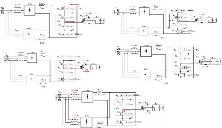
The converter and its key waveforms are shown in Figs. 2 and 3, respectively. The proposed converter uses auxiliary windings that are taken from the converter transformer to act as “magnetic switches” to cancel the dc bus capacitor voltage so that the voltage that appears across the diode bridge output is zero. Auxiliary Winding 1 (Naux1/N1 = 2) cancels out the dc bus voltage when the primary voltage of the main transformer is positive, so that the output voltage of Diode Bridge 1 (DB1 ) is zero, and the currents in input inductors La1, Lb1, and Lc1 rise. Auxiliary Winding 2 (Naux2/N1 = 2) cancels out the dc bus voltage when the primary voltage of the main transformer is negative, so that the output voltage of Diode Bridge 2 (DB2 ) is zero, and the currents in input inductors La2, Lb2, and Lc2 rise.
When there is no voltage across the main transformer primary winding, the total voltage across the dc bus capacitors appears at the output of the diode bridges, and the input currents falls since this voltage is greater than the input voltage. If the input currents are discontinuous, the envelope of the input current will be sinusoidal and in phase with the input voltages. The converter has the following modes of operation during a half switching cycle; equivalent circuit diagrams that show the converter’s modes of operation are shown in Fig. 4:
Mode 1 (t0 ≤ t ≤ t1 ): During this interval, switches S1 and S2 are ON. It should be noted that both dc bus capacitors and the flying capacitor are charged to half of the dc bus voltage. In this mode, energy from dc bus capacitor C1 flows to the output load. Due to magnetic coupling, a voltage appears across Auxiliary Winding 1 that is equal to the dc bus voltage, but with opposite polarity. This voltage cancels the total dc bus capacitor voltage so that the voltage at the diode bridge output is zero, and the input currents in La1, Lb1, and Lc1 rise.
Mode 2 (t1 ≤ t ≤ t2 ): In this mode, S1 is OFF, and S2 remains ON. Capacitor Cs1 charges and capacitor Cs4 discharges through Cf until the voltage across Cs4 , the output capacitance of S4 , is clamped to zero. The energy stored in the input inductor during the previous mode starts being transferred into the dc bus capacitors. This mode ends when S4 turns ON with ZVS.
ISSN (Print) : 2320 – 3765 ISSN (Online): 2278 – 8875
I
nternational
J
ournal of
A
dvanced
R
esearch in
E
lectrical,
E
lectronics and
I
nstrumentation
E
ngineering
(An UGC Approved Journal)
Website: www.ijareeie.com
Vol. 6, Issue 8, August 2017
Fig. 4. Modes of operation. (a) Mode 1 (t0 < t < t1 ). (b) Mode 2 (t1 < t < t2 ). (c) Mode 3 (t2 < t < t3 ). (d) Mode 4 (t3 < t < t4 ). (e) Mode 5 (t4 < t < t5 ).
Mode 4 (t3 ≤ t ≤ t4 ): In this mode, S1 and S2 are OFF. The energy stored in L1 continues to be transferred into the dc bus capacitor. The primary current of the transformer discharges the output capacitor of Cs3 . If there is enough energy in the leakage inductance, the primary current will completely discharge the body capacitor of Cs3 , and current will flow through the body diode of S3.This current also chargesC2 through the body diodes of S3 and S4 . Switch S3 is switched ON at the end of this mode.
Mode 5 (t4 ≤ t ≤ t5 ): In this mode, S3 and S4 are ON, and energy flows from capacitor C2 to the load. A voltage appears across Auxiliary Winding 2 that is equal to the dc bus voltage, but with opposite polarity to cancel out the dc bus voltage. The voltage across the boost inductors L2 (L2 = Labc2) becomes only the rectified supply voltage of each phase, and the current flowing through each inductor increases. This mode ends when the energy stored in L1 is completely transferred into the dc bus capacitor. For the remainder of the switching cycle, the converter goes through Modes 6–10, which are identical to Modes 1–5 except that S3 and S4 are ON instead of S1 and S2 and DB2 conducts current instead of DB1 .
The input current is the sum of currents iL1 and iL2, corresponding to each set of input inductors, with each inductor having a discontinuous current. However, by selecting appropriate values for La1 = Lb1 = Lc1 and La2 = Lb2 = Lc2, two inductor currents such as iLa1 and iLa2 can be made to overlap each other so that the input current can be made continuous, thus reducing the size of input filter significantly.
There is a natural 180° phase difference between the currents in L1 and the currents in L2 as one set of currents rises when the transformer primary is impressed with a positive voltage, and the other set rises when the transformer primary is impressed with a negative voltage.
It should be noted that standard phase-shift PWM can be implemented in the converter, and thus, a standard phase-shift PWM IC can be used to generate the gating signal. This can be seen from Fig. 3 and the modal circuit diagrams. Switches S2 and S3 are not allowed to be ON at the same time, and switches S1 and S4 are not allowed to be ON simultaneously as well.
ISSN (Print) : 2320 – 3765 ISSN (Online): 2278 – 8875
I
nternational
J
ournal of
A
dvanced
R
esearch in
E
lectrical,
E
lectronics and
I
nstrumentation
E
ngineering
(An UGC Approved Journal)
Website: www.ijareeie.com
Vol. 6, Issue 8, August 2017
The sequence of alternating energy transfer and freewheeling modes that occur during a switching cycle corresponds to the
Fig. 5. Flying capacitor versus diode-clamped three-phase single-stage converter. (a) Mode 2 in the proposed flying capacitor converter (t1 < t < t2 ) (b) Mode 2 in diode-clamped converter (t0 < t < t1 ).
same sequence of modes that exists in a standard two-level phase-shift PWM full-bridge converter.
III. FLYING CAPACITOR VERSUS DIODE-CLAMPED MULTILEVEL THREE-PHASE SINGLE-STAGE CONVERTER
The proposed interleaved topology with flying capacitor can guarantee a ZVS turn-on for its very top and very bottom switches in a way that the converter presented in [17] cannot. To understand why this is so, first consider a standard two-level ZVS-PWM dc–dc full-bridge converter operating with phase shift PWM. For this converter, the leading leg switches (switches that are turned ON when the converter enters a freewheeling mode of operation) of this converter can be turned ON with ZVS. This is due to the fact that the transformer primary current is dominated by reflected output inductor current during this transition so that there is sufficient energy available to turn ON the leading leg switches with ZVS. It is the lagging leg switches (switches that are turned ON when the converter is exiting a freewheeling mode) that lose their ability to turn ON with ZVS under light-load conditions as it is only the transformer primary leakage inductance energy that is available to discharge and charge the appropriate switch output capacitances.
Now consider the converter proposed in [17], as shown in Fig. 5(b). It can be seen in Fig. 5(a) that the converter enters a freewheeling mode of operation when switch S1 is turned OFF. The converter exits this freewheeling mode by the turning OFF of S1 and then the simultaneous turning ON of switches S3 and S4. During this transition, it is only the leakage inductance energy that is available to turn S3 and S4 ON with ZVS. Similarly, switch S1 and S2 are turned ON when the converter exits the other freewheeling mode of the switching cycle, again, with only the leakage inductance energy available to discharge their output capacitances. What this means is that all the converter switches lose the ability to turn ON with ZVS under light-load conditions as only leakage inductance energy is available to discharge their output capacitances just before they are turned ON. With respect to the proposed converter, as can be seen from Mode 2 (just like Mode 7), shown in Fig. 5(a), when S1 (or S4 ) turns OFF and the converter enters a freewheeling mode of operation, the energy available to charge the output capacitance of S1 (or S4 in Mode 7) and discharge the output capacitance of S4 (or S1 in Mode 7) is the energy stored in leakage inductance plus the energy in output filter inductor that is “reflected” to the primary. Since the energy in the filter inductor is large compared to that required to charge/discharge the capacitances, the body capacitance of S4 (or S1 in Mode 7) can be discharged completely through flying capacitor Cf . Once this happens, switch S4 (or S1 afterMode 7) can be turned ON with ZVS in anticipation for later on in the switching cycle when the converter exits a freewheeling mode of operation.
ISSN (Print) : 2320 – 3765 ISSN (Online): 2278 – 8875
I
nternational
J
ournal of
A
dvanced
R
esearch in
E
lectrical,
E
lectronics and
I
nstrumentation
E
ngineering
(An UGC Approved Journal)
Website: www.ijareeie.com
Vol. 6, Issue 8, August 2017
mode of operation. These switches can only turn ON with ZVS if there is sufficient transformer leakage inductance energy to discharge the output capacitance of these devices when the converter is exiting a freewheeling mode of operation. Since this is rarely the case when the converter is operating under light-load conditions, these switches will not turn ON with ZVS. As a result, the proposed converter with flying capacitor has better light-load efficiency than the converter proposed in [17] because two of its switches can always turn ON with ZVS, regardless of the load.
IV. CONVERTER ANALYSIS & SELF TUNED PID using GENETIC ALGORITHM OPERATION
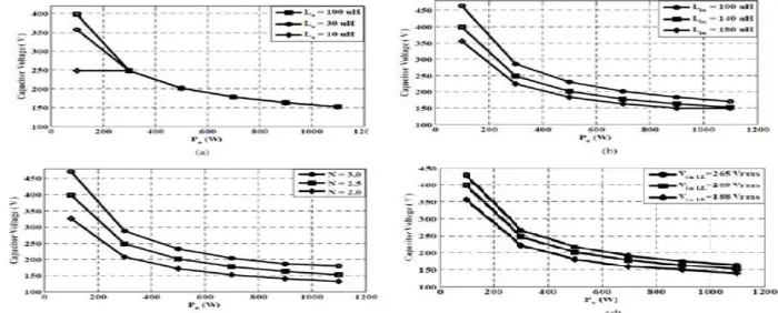
The analysis and design of the proposed converter are almost identical to that presented in [16] and [17] and therefore are not presented here in detail. Only graphs of key characteristic curves and general design guidelines are presented in this paper.
Fig. 6. Steady-state characteristic curves (Vin = 208 Vrms , Vo = 48 V, fsw = 100 kHz. (a) Effect of output inductor value Lo on dc bus voltage. (b) Effect of input inductor value Lin on dc bus voltage. (c) Effect of transformer ratio
value N on dc bus voltage. (d) Effect of input voltage vin on dc bus voltage.
The reader is referred to [16] and [17] for details. In order to analyze and determine the steady-state operating points of the converter, a computer program such as the one presented in [16] has been used. Graphs of steady-state characteristics, such as the ones shown in Fig. 6, can be used as part of a design procedure. These graphs help to find out the appropriate parameter values based on the defined operating point. Assuming ideal operation to simplify the analysis, the characteristic curves of the proposed converter and the converter proposed in [17] are the same? This is because in this case, the Flying capacitor just affects the transition modes of the converter and does not affect the overall steady-state operation of the proposed converter.
Genetic Algorithm Operation
Artificial intelligence techniques have come to be the most widely used tool for solving many optimization problems. GA is a relatively new approach of optimun searching (Mitchell, 1999), becoming increasingly popular in science and engineering disciplines. GA inherits its ideas from evolution of the nature. Even a simple GA algorithm appears to be robust, and the complexity of algorithm and result of GA is irrelevant to the length of genetic string and the original state of population. GA is so simple that it only involves some selection, crossover and mutation operations, but it is so efficient that it can find a nearly optimum solution even for a large scale problem (Mitchell, 1999).
ISSN (Print) : 2320 – 3765 ISSN (Online): 2278 – 8875
I
nternational
J
ournal of
A
dvanced
R
esearch in
E
lectrical,
E
lectronics and
I
nstrumentation
E
ngineering
(An UGC Approved Journal)
Website: www.ijareeie.com
Vol. 6, Issue 8, August 2017
the optimal solution through several generations, the reproduction use crossover fraction of 0,6 with 2 elite count, the mutation function is adaptive feasible, and the crossover function is scattered. The objective function to minimize equation (5) was constructed using parameters of the response to step of the system, considering the magnitudes of the variables.
(1) Where:
● Tr = Rise time [s].
● Ess = Steady-state error [V].
● Ts = Settling Time [s].
● Mpu = Overshoot [V].
● Imax = Current maximum in the inductor [A].
V. DESIGN GUIDELINES & SIMULINK RESULTS AND OUTPUTS
General considerations that should be taken into account when trying to design the proposed converter are discussed in this section of the paper. The key parameters values in the design of the converter are output inductor Lo , transformer turns ratio N, and input inductor Lin . The following should be considered when trying to select values for these components:
A. Transformer Turns Ratio N The value of N affects the primary-side dc bus voltage. It determines how much reflected load current is available at the transformer primary to discharge the bus capacitors. If N is low, the primary current may be too high, and thus, the converter will have more conduction losses. If N is very high, then the amount of current circulating in the primary side is reduced, but the primary current that is available to discharge the dc-link capacitors may be low, and thus, dc bus voltage may become excessive under certain operating conditions (i.e., high line). The minimum value of N can be found by considering the case when the converter must operate with minimum input line and, thus, minimum primary-side dc bus voltage and maximum duty cycle. If the converter can produce the required output voltage and can operate with discontinuous input and continuous output currents in this case, then it can do so for all cases.
B. Output Inductor Lo The output inductor should be designed so that the output current is made to be continuous under most operating conditions, if possible. The minimum value of Lo should be the value of Lo with which the converter’s output current will be continuous on the when the converter is operating with maximum input voltage, minimum duty cycle, and minimum load. If this condition is met, then the output current will be continuous for all other converter’s operating conditions. On the other hand, the value of Lo cannot be too high as the dc bus voltage of the converter may become excessive under very light-loads conditions.
C. Input inductor Lin : The value for L1 and L2 should be low enough to ensure that their currents are fully discontinuous under all operating conditions, but not so lowas to result in excessively high peak currents. It should be noted that input current is summation of inductor currents iL1 and iL2 which are both discontinuous. However, by selecting appropriate values for L1 (= La1 = Lb1 = Lc1 ) and L2 (= La2 = Lb2 = Lc2 ) in such a way that two inductor currents such as iLa1 and iLa2 have to overlap each other, the input current can be made.
D. Flying Capacitor Cf The flying capacitor is charged to half of the dc bus voltage.
When the converter is operated with phase-shift PWM control, as shown in Fig. 3, Cf is generally decoupled from the converter except during certain switching transitions, such as when S1 is turned OFF to start Mode 2 and when S4 is turned OFF during the equivalent mode later in the switching cycle; therefore, there is little opportunity for Cf to charge and discharge during a switching cycle. As a result, the converter can be designed according to the design procedure given in [17] as the operation of the two converters is very similar.
ISSN (Print) : 2320 – 3765 ISSN (Online): 2278 – 8875
I
nternational
J
ournal of
A
dvanced
R
esearch in
E
lectrical,
E
lectronics and
I
nstrumentation
E
ngineering
(An UGC Approved Journal)
Website: www.ijareeie.com
Vol. 6, Issue 8, August 2017
(2)
where Io is output current, Dmax is maximum duty cycle, N is transformer turns ratio, fs is switching frequency, and
ΔVCf is the peak-to-peak ripple voltage of Cf . For maximum load Po = 1.1 kW and output voltage Vo = 48 V, the output current is Io = 23 A. If the maximum duty cycle is assumed to be Dmax = 0.4, the transformer turns ratio is N =
2.5, and the switching frequency is fsw = 100 kHz, then a 0.5% ripple for flying capacitor voltage results in ΔVCf =
0.005 × 400 = 2 V so that the minimum value for Cf according to (1) is Cf = 4.6 μF
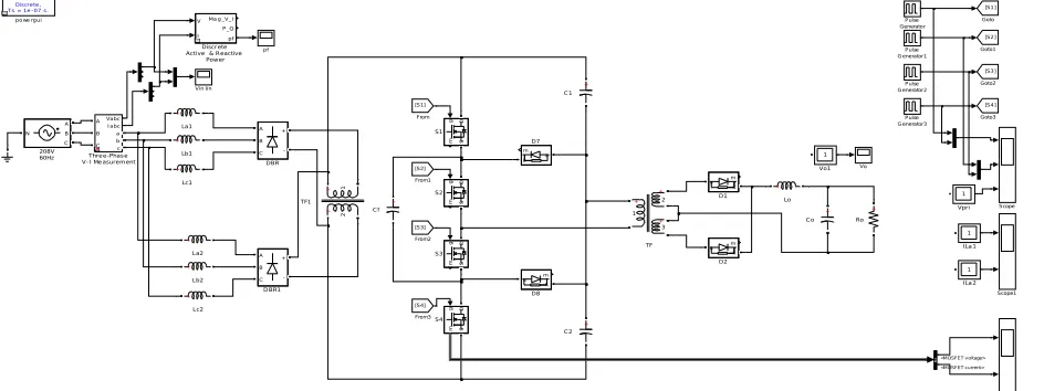
Fig 7 MATLAB/Simulink Model of the Proposed Three phase Interleaved PFC Converter
(a) (b)
Fig8. Simulation Waveforms of (a) Vg1,Vg2,Vg3,Vg4 & Primary Voltage (b) Inductor Currents Il1 ,Il2
Discre te , Ts = 1e -07 s.
powe rgui p f 1 Vpri 1 Vo1 Vo Vin Iin Vabc Iabc A B C a b c Thre e-Phas e V-I Me asurem ent
1 2 + + TF1 1 2 3 + + + TF Scope2 Scope1 Scope g m D S S4 g m D S S3 g m D S S2 g m D S S1 + Ro Pulse G enerator3 Pulse G enerator2 Pulse G enerator1 Pulse Generato r + Lo + Lc2 + Lc1 + Lb2 + Lb1 + La2 + La1 1 ILa 2 1 ILa 1 [S4 ] Goto3 [S3 ] Goto2 [S2 ] Goto1 [S1 ] Goto [S4] From3 [S3] From2 [S2] From1 [S1] From V I Ma g_V_I P_Q pf Discr ete Active & R eactive
Power A B C + -D BR1 A B C + -DBR m a k D8 m a k D7 m a k D2 m a k D1 + C o + C f + C 2 + C 1 N A B C 208V 60Hz
ISSN (Print) : 2320 – 3765 ISSN (Online): 2278 – 8875
I
nternational
J
ournal of
A
dvanced
R
esearch in
E
lectrical,
E
lectronics and
I
nstrumentation
E
ngineering
(An UGC Approved Journal)
Website: www.ijareeie.com
Vol. 6, Issue 8, August 2017
Fig9. Simulation Waveforms of Converter Output Voltage (Vo)
ISSN (Print) : 2320 – 3765 ISSN (Online): 2278 – 8875
I
nternational
J
ournal of
A
dvanced
R
esearch in
E
lectrical,
E
lectronics and
I
nstrumentation
E
ngineering
(An UGC Approved Journal)
Website: www.ijareeie.com
Vol. 6, Issue 8, August 2017
Fig11. Simulation Waveforms of Input Voltage (Vin) & Input Current (Is)
VI. CONCLUSION
In this paper we proposed a new hybrid algorithm for the regulation of voltage of the boost converter, and the active correction of the power factor. The algorithm integrates the main features of the current mode control (dynamic response, stability and PFC), and the reliability and design of PID controls. As alternative of optimal adjustment of the parameters of loop PID, considering the problem of combination and optimization of muti-variables, intends to use a genetic algorithm whose objective function is evaluated on the parameters of the answer of the model calculated from the average model of the boost converter. The scheme of control proposed was evaluated successful by simulation and on a laboratory prototype of 200 W, having demonstrated its viability and high performance in terms of output voltage regulation and PFC. An interleaved three-phase, three-level, and PFC ac–dc converter using standard phase-shift PWM was presented in this paper. In this paper, the operation of the converter was explained, and its feasibility was confirmed with experimental results obtained from a prototype converter. The efficiency of the new converter was compared to that of another converter of the same type. It was shown that the proposed converter has a better efficiency, especially under light-load conditions, and it was explained that this is because energy from the output inductor can always be used to ensure that the very top and the very bottom switches can be turned ON with ZVS, due to a discharge path that is introduced by its flying capacitor.
FUTURE SCOPE
This paper future extended on to design the controller parameters of the conventional Power Factor Correction (PFC) converter. The dynamics of the converter is nonlinear & Electrical Drive loads therefore, it is hard to derive desirable performance. Genetic algorithm is used to optimize the control parameters of PFC converter.
REFERENCES
[1] Limits for Harmonic Current Emission (Equipment Input Current>16A per Phase), IEC1000-3-2, 1995.
ISSN (Print) : 2320 – 3765 ISSN (Online): 2278 – 8875
I
nternational
J
ournal of
A
dvanced
R
esearch in
E
lectrical,
E
lectronics and
I
nstrumentation
E
ngineering
(An UGC Approved Journal)
Website: www.ijareeie.com
Vol. 6, Issue 8, August 2017
[3] H. S. Ribeiro and B. V. Borges, “New optimized full-bridge single-stage ac/dc converters,” IEEE Trans. Ind. Electron., vol. 58, no. 6, pp. 2397– 2409, Jun. 2011.
[4] N. Golbon and G. Moschopoulos, “A low-power ac-dc single-stage converter with reduced dc bus voltage variation,” IEEE Trans. Power Electron., vol. 27, no. 8, pp. 3714–3724, Jan. 2012.
[5] H. Ma, Y. Ji, and Y. Xu, “Design and analysis of single-stage power factor correction converter with a feedback winding,” IEEE Trans. Power Electron., vol. 25, no. 6, pp. 1460–1470, Jun. 2010.
[6] S. Dusmez and A. Khaligh, “A charge-nonlinear-carrier-controlled reduced-part single-stage integrated power electronics interface for automotive applications,” IEEE Trans. Veh. Technol., vol. 63, no. 3, pp. 1091– 1103, Mar. 2014.
[7] R. Ramakumar and P. Chiradeja, “Distributed generation and renewable energy systems,” in Proc. 37th Intersoc. Energy Convers. Eng. Conf. , 2002, pp. 716–724.
[8] S. I. Mustapa, Y. P. Leong, and A. H. Hashim, “Issues and challenges of renewable energy development: A Malaysian experience,” in Proc. Int. Conf. Energy Sustainable Develop.: Issues Strategies, 2010, pp. 1–6.
[9] W. Kempton and S. Letendre, “Electric vehicles as a new power source for electric utilities,” Transp. Res. Part D, Transport Environ., vol. 2, pp. 157–175, 1997.
[10] B. Kramer, S. Chakraborty, and B. Kroposki, “A review of plug-in vehicles and vehicle-to-grid capability,” in Proc. IEEE Ind. Electron., 2008, pp. 2278–2283.
[11] U. K. Madawala, P. Schweizer, and V. V. Haerri, ““Living and mobility”— A novel multipurpose in-house grid interface with plug-in hybrid blue angel,” in Proc. IEEE Conf. Sustainable Energy Technol., 2008, pp. 531–536.
[12] U. K. Madawala and D. J. Thrimawithana, “A bidirectional inductive power interface for electric vehicles in V2G systems,” IEEE Trans. Ind. Electron., vol. 58, no. 10, pp. 4789–4796, Oct.2011.
[13] D. J. Thrimawithana, U. K. Madawala, R. Twiname, and D. M. Vilathgamuwa, “A novel matrix converter based resonant dual active bridge for V2Gapplications,” in Proc. IPEC Conf. Power Energy, 2012, pp. 503–508.
[14] D. C. Erb, O. C. Onar, and A. Khaligh, “An integrated bi-directional power electronic converter with multi-level AC-DC/DC-AC converter and non-inverted buck-boost converter for PHEVs with minimal grid level disruptions,” in Proc. IEEE Vehicle Power Propulsion Conf., 2010, pp. 1–6. [15] R. L. Steigerwald, R.W.DeDoncker, andH.Kheraluwala, “A comparison of high-power DC-DC soft-switched converter topologies,” IEEE Trans. Ind. Appl., vol. 32, no. 5, pp. 1139–1145, Sep./Oct. 1996.
[16] J. Walter and R. W. De Doncker, “High-power galvanically isolated DC/DC converter topology for future automobiles,” in Proc. IEEE 34th Annu. Power Electron. Spec. Conf., 2003, vol. 1, pp. 27–32.
[17] N. D.Weise, K. Basu, and N. Mohan, “Advanced modulation strategy for a three-phase AC-DC dual active bridge for V2G,” in Proc. IEEE Vehicle Power Propulsion Conf., 2011, pp. 1–6.
[18] N. D.Weise, K. K. Mohapatra, and N.Mohan, “Universal utility interface for plug-in hybrid electric vehicles with vehicle-to-grid functionality,” in Proc. IEEE Power Energy Soc. Gen. Meeting, 2010, pp. 1–8.
[19] D. Yu, S. Lukic, B. Jacobson, and A. Huang, “Review of high power isolated bi-directional DC-DC converters for PHEV/EV DC charging infrastructure,” in Proc. IEEE Energy Convers. Congr. Expo., 2011, pp. 553–560.
[20] Z. Biao, S. Qiang, L. Wenhua, and S. Weixin, “Current-stress-optimized switching strategy of isolated bidirectional DC-DC converter with dualphase- shift control,” IEEE Trans. Ind. Electron., vol. 60, no. 10, pp. 4458– 4467, Oct. 2013.
[21] Z. Biao, Y. Qingguang, and S. Weixin, “Extended-phase-shift control of isolated bidirectional DC-DC converter for power distribution in microgrid,” IEEE Trans. Power Electron., vol. 27, no. 11, pp. 4667–4680, Nov. 2012.
[22] B. Hua, N. Ziling, and C. C. Mi, “Experimental comparison of traditional phase-shift, dual-phase-shift, and model-based control of isolated bidirectional DC-DC converters,” IEEE Trans. Power Electron., vol. 25, no. 6, pp. 1444–1449, Jun. 2010.
[23] A. K. Jain and R. Ayyanar, “PWM control of dual active bridge: Comprehensive analysis and experimental verification,” IEEE Trans. Power Electron., vol. 26, no. 4, pp. 1215–1227, Apr. 2011.
[24] F. Krismer and J. W. Kolar, “Closed form solution for minimum conduction loss modulation of DAB converters,” IEEE Trans. Power Electron., vol. 27, no. 1, pp. 174–188, Jan. 2012.