Three Phase Five Level Pulse Width
Modulated Cascaded Switched Voltage Source
Inverter:A Review
Anuj Kumar
PG Student [EPES], Dept. of EE, Ajay Kumar Garg Engineering Engineering College, Ghaziabad, Uttar Pradesh, India
ABSTRACT:A three phase five level pulse width modulated cascaded switched voltage source inverter topology has two cascaded units in each phase leg and the cascaded units called H-bridge. Switch legs of these H-bridge are separated by a balancing capacitor or switched capacitor and a diode. The upper three H-bridge modules in the topology have distinct dc input voltage source and the lower three H-bridge modules have a common dc input voltage source. To generate gating signals for power semiconductor switched a single carrier sinusoidal pulse width modulation (SC-PWM) is employed. SC-PWM is hybridised so that the output voltage of three phase five level pulse width modulated cascaded switched voltage source inverter inherit features of switching losses reduction from Fundamental Pulse Width Modulation (FPWM) and better harmonic performance from Multiple Sinusoidal Pulse Width Modulation (MSPWM). In order to overcome uneven switching losses, a sequential switching scheme is interpolate with the already employed Hybrid modulation. Further to obtain resultant Sequential Switching Hybrid Pulse Width Modulation (SSHPWM), a simple PWM is also introduced that balances dissipation of power among the two cascaded H-bridge power modules.
KEYWORDS: Total Harmonic Distortion, Hybrid Modulation Scheme.
I. INTRODUCTION
For more than four decades since 1975 as the multi level converter's concept given by R.H Baker & L.H Bannister (1975), multilevel converters have been in under research and development and have established successful applications in industry. Multilevel term begins with three level. The first three level converter is given by A. Nabae, I. Takahashi & H. Akagi (1981). However there is still a technology under development and there are several new commercial topologies which have been reported in the last certain years given by R.H Baker (1981), P.W Hammond (1977), F.Z Peng & J.S Lai (1997), P.W Hammond (2000), M.F Aiello, P.W Hammond & M Rastogi (2001), J.P Lavieville, P. Carrere & T Meynard (1997) (1998), T.A Meynard & H. Foch (1992). To achieve higher power, multilevel has eliminatory concept, is to use a series of switches with several dc voltage sources. Conventional multilevel topologies have undesirable features such as over-voltage problem, fluctuations, link voltage controller, several isolated dc voltage source and so on. To reduce these conventional multilevel inverters drawbacks, a three-level pulse width modulated switched voltage source inverter is given by W.S Oh, S.K Han, S.W Choi & G.W Moon (2005). In this topology, each phase leg has two switches one is flying capacitor and other one is diode. The three level output of this topology is VS, 0, -VS. This topology does not have voltage imbalance problem as given by B.R Lin (2000) and
which can be achieved by the use of multiple dc-levels. Nowadays, multilevel inverter have received huge attention for medium voltage and high power applications. The present work provide an efficient topology which suits for medium voltage and high power applications.
II. OPERATION AND CIRCUIT CONFIGURATION
The Three phase five level PWM cascaded SVS Inverter is a hybrid of Three-level Switched Voltage Source Inverter and Cascaded Multilevel Inverter is shown in Fig. 1. The H-bridge modules in upper side of Switched Voltage Source Inverter have separate dc voltage sources whereas The lower side modules share a common dc voltage source. Proper switching of any H-bridge inverter module can generate three output voltage levels: Vs, 0, -Vs. In each phase leg a maximum five output voltage level can be generated: 2Vs, Vs, 0, -Vs, -2Vs. At the load terminal nine output line to line voltage are generated.
Fig. 1: Circuit arrangement of three phase five level PWM cascaded SVS inverter Circuit arrangement of three phase five level PWM cascaded SVS inverter
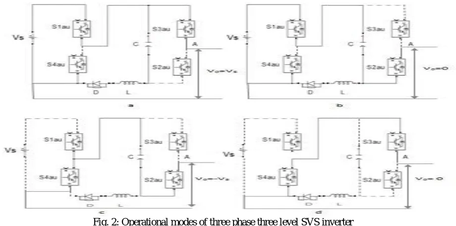
0V in first and second periods of the output voltages. The switching states of active power semiconductor switches corresponding to the synthesised output are summarised in Table 1 & 2.
Fig. 2: Operational modes of three phase three level SVS inverter
Table 1: Switching states of phase 'a' of three phase five level pulse width modulated cascaded SVS Inverter for first period
Phase Voltage
V0
Switching States First Period
S1aU S2aU S3aU S4aU S1aD S2aD S3aD S4aD
2VS 1 0 1 0 1 0 1 0
VS 1 0 1 0 0 0 0 0
0 1 1 0 0 0 0 1 1
-VS 0 1 0 1 0 0 0 0
-2VS 0 1 0 1 0 1 0 1
Table 2 : Switching states of phase 'a' of three phase five level pulse width modulated cascaded SVS Proposed Inverter for second period
Phase Voltage
V0
Switching States Second Period
S1aU S2aU S3aU S4aU S1aD S2aD S3aD S4aD
2VS 1 0 1 0 1 0 1 0
VS 1 0 1 0 0 0 0 0
0 0 0 1 1 0 0 0 0
-VS 0 1 0 1 0 0 0 0
III. MODULATION SCHEME
Single carrier sinusoidal PWM (SC-PWM) is a resultant of multi sinusoidal reference signals with a frequency of f0
(fundamental) and amplitude of Vm and one carrier signal. Number of sinusoidal reference signals require according to
number of converter cells. Carrier signal is a train of triangular waveform with desired frequency of fc and amplitude of VC. The N-level SC-SPWM needs M modulation signals that have same frequency f0 and amplitude Vm with a DC bias
of VC as difference between them. M is given by
= {( −1) 2⁄ }
where N is number of levels
Amplitude modulation index (Ma) and Frequency modulation index (Mf) is given by
=
=
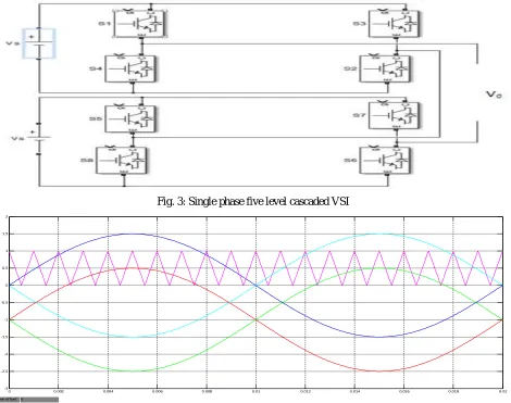
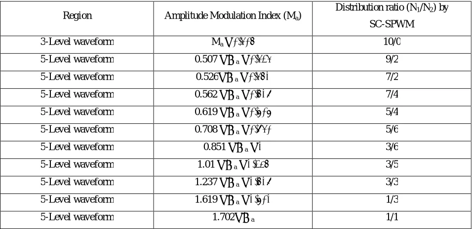
It is observe from Fig. 4 that switching transition distribution's is determined by Amplitude modulation index (Ma). N1
is the number of switching transition that occur between 0 level to 1st level and N2 is the number of switching transition
that occur between 1st level to 2nd level.
Fig. 3: Single phase five level cascaded VSI
Fig. 4: SC-SPWM technique
0 0.002 0.004 0.006 0.008 0.01 0.012 0.014 0.016 0.018 0.02
Fig. 5: Output Voltage waveform of single phase five level cascaded VSI
Table 3: Summary of switching transition distribution defined by SC-SPWM against amplitude modulation index (Ma)
with frequency ratio (Mf = 1000Hz)
Region Amplitude Modulation Index (Ma)
Distribution ratio (N1/N2) by
SC-SPWM
3-Level waveform Ma ≤ 0.506 10/0
5-Level waveform 0.507 ≤ Ma ≤ 0.525 9/2
5-Level waveform 0.526≤ Ma ≤ 0.561 7/2
5-Level waveform 0.562 ≤ Ma ≤ 0.618 7/4
5-Level waveform 0.619 ≤ Ma ≤ 0.707 5/4
5-Level waveform 0.708 ≤ Ma ≤ 0.850 5/6
5-Level waveform 0.851 ≤ Ma ≤ 1 3/6
5-Level waveform 1.01 ≤ Ma ≤ 1.236 3/5
5-Level waveform 1.237 ≤ Ma ≤ 1.618 3/3
5-Level waveform 1.619 ≤ Ma ≤ 1.701 1/3
5-Level waveform 1.702≤ Ma 1/1
Two switching states are used for generation of 0 V in first and second period with the help of hybrid modulation employed in the switching scheme. Hybrid modulation technique is the combination of fundamental frequency pulse-width modulation (FPWM) and multi-sinusoidal pulse-pulse-width modulation (MSPWM), so that output inherits features of switching loss reduction form FPWM and good harmonic performance from MSPWM. Logic signals A and B as shown in Fig are used at fundamental frequency fm to hybridise the modulation technique herein. A sequential
switching scheme is embedded with the employed hybrid modulation to overcome unequal switching losses and therefore differential heating among power semiconductor devices in H-bridges because it is important to share power loss to every power semiconductor device in a cell/unit and furthermore among all the cascaded modules for long operating time expectancy. The logic signals C and D as shown in Fig at half of the fundamental frequency (fm/2) are
used to equalise the switching losses and make every power semiconductor switch operating at MSPWM and FPWM in each H-bridge to have equal power loss. A resultant sequential switching hybrid pulse-width modulation (SSHPWM) is
0 0.002 0.004 0.006 0.008 0.01 0.012 0.014 0.016 0.018 0.02
obtain by introducing a simple base pulse-width modulation (PWM) scheme that balances dissipated power among two cascaded h-bridge modules in all the three phase legs. The logic signals E and F at 1/4th of fundamental frequency (fm/4)
are used to achieve this balances of power dissipation for phase a.
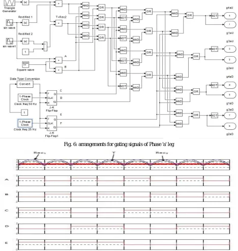
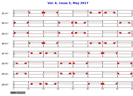
The basic principle behind generating gate signals begin with comparison of modulating signals with the carrier wave. In actual gate signals are generated by logical combinations of the results of the comparisons and the base square waveform having frequencies of (fm), (fm/2) and (fm/4). The first square wave at frequency (fm ) can be easily obtained
from J-K flip-flops configures in toggle mode and clocked at frequency of (2fm). Similarly second square wave at
frequency (fm/2) and third square wave at frequency (fm/4) can be easily obtained from J-K flip-flop configures in toggle
mode and clocked at frequency of (fm) and (fm/2) respectively.
The gating signals of phase a are given by the use of logical AND, OR, NOT gates.
= ⎣ ⎢ ⎢ ⎢ ⎢ ⎢
⎡ {( > )∗ } + ∗
+ {( > )∗ } + ∗ ∗
+ {( > )∗ } + ∗
+ {( > )∗ } + ∗
∗ ⎦ ⎥ ⎥ ⎥ ⎥ ⎥ ⎤ = ⎣ ⎢ ⎢ ⎢ ⎢ ⎢
⎡ {( > )∗ } + ∗
+ {( > )∗ } + ∗ ∗
+ {( >
)∗ } + ∗
+ {( > )∗ } + ∗
∗ ⎦ ⎥ ⎥ ⎥ ⎥ ⎥ ⎤ = = = ⎣ ⎢ ⎢ ⎢ ⎢ ⎢
⎡ {( > )∗ } + ∗
+ {( > )∗ } + ∗ ∗
+ {( >
)∗ } + ∗
+ {( > )∗ } + ∗ ∗ ⎦⎥
⎥ ⎥ ⎥ ⎥ ⎤ = ⎣ ⎢ ⎢ ⎢ ⎢ ⎢
⎡ {( > )∗ } + ∗
+ {( > )∗ } + ∗ ∗
+ {( > )∗ } + ∗
+ {( > )∗ } + ∗
=
Fig. 6: arrangements for gating signals of Phase 'a' leg
Fig. 8:Gating signals for phase 'a' leg
IV. NEED OF SNUBBER INDUCTOR
The Capacitor C is charged to a constant input voltage VS and hence regard as a constant voltage source but in real time
operation a slight difference between the real capacitor voltage (VC) and the dc input voltage (VS). This difference may
cause an inrush current on switch S1aU and diode when switch turn on. This inrush current is avoided by placing a small
snubber inductor L between diode and capacitor. Operation of three phase five level pulse width modulated cascaded switched voltage source inverter does not affect by placing of inductor.
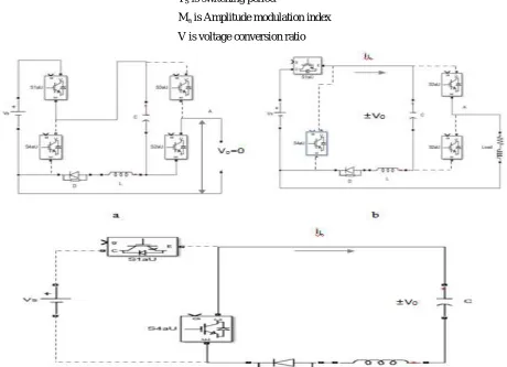
Fig. 8 shows one of the switching circuits of switched voltage source inverter given in Fig. 2 depicting buck operation. The snubbber inductor L is quite small and buck converter circuits in Fig. 8a and 8b operate in discontinuous conduction mode. In this mode of operation, V (voltage conversion ratio) is given by
= = 2
1 + {1 + (8 ⁄ )}
where = ( ⁄ )
TS = switching period
The design equation of L is given by
= 8
2
−1 −1
= (1− )
8
2
−1 −1
where VC is Capacitor Voltage
IL is inductor current
TS is switching period
Ma is Amplitude modulation index
V is voltage conversion ratio
Fig. 9: Operation of SVS inverter module depicting buck converter a Half-bridge leg of Phase 'a'
The value of balancing capacitor in Farad is given according to the impedance of load connected means there is no change in the impedance value whether capacitor is working or not because load current value remain almost constant throughout the working of inverter. So when S2, S4 will on in second half of first period, balancing capacitor acts as source and feed the load. After Switching on of S1, S4 gets off and capacitor starts charging. An inrush current will flow through switch S1 due to negligible resistance of capacitor and switch will damage. To avoid this situation snubber inductor L as indicate above is connected between diode and capacitor and derived according to above formula where other values are R = 20Ω, VC = 100 V, TS = 3.33e-4 sec, Ma = 2, V = 0.9, IL = 6.36A consider for simulation.
V. SIMULATION RESULT AND DISCUSSION
Matlab Simulink Simulation has done for the operational principles of three phase five level pulse width modulated cascaded switched voltage source inverter as shown in Fig. 6, Fig. 7 for phase 'a', and for switching scheme as shown in Table 1 and Table 2.
A balanced three phase star connected R-L load with 20 Ω resistance and 63.98 mH inductance per phase were used. Load power factor is 0.705 and balancing capacitor C of value 31.8 mF and snubber inductor of value 0.32 mH were used as calculated. Single carrier triangular wave of 3 KHz frequency and input voltage of 100V were used.
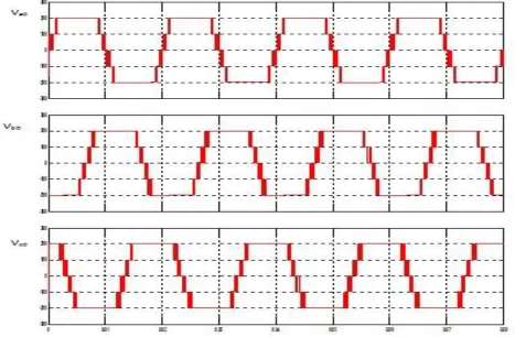
The Output phase voltage waveforms exhibit five levels: 2VS, VS, 0 -VS, -2VS as shown below.
Fig 11: Output line voltage waveforms of three phase five level pulse width modulated cascaded SVS inverter Below table shows the THD% in Output Line and Phase voltages waveform of three phase five level pulse width modulated cascaded switched voltage source inverter at different Amplitude Modulation Index (Ma).
Table 4: Summary of THD% against Amplitude Modulation Index (Ma) of three phase five level pulse width
modulated cascaded SVS inverter
Amplitude Modulation Index (Ma)
THD(%)
Line Voltage Phase Voltage
0.5
41.28%
53.29%
1
21.67%
27.43%
1.25
14.86%
22.03%
1.5
13.32%
23.14%
2
12.26%
27.07%
2.5
13.85%
30.72%
3
15.72%
32.79%
Fig. 12: Graph of THD% against Amplitude modulating index (Ma)
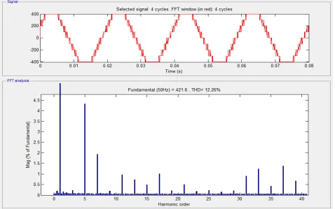
Harmonic spectrum of one of line voltage waveform is done wherein THD of value 12.26% is achieved at Amplitude modulation index (Ma) = 2.
VI. CONCLUSION
In the thesis a brief summary of three phase five level pulse width modulated cascaded SVS inverter has provided with less number of input dc voltage source for both medium and high power application.
The three phase five level PWM cascaded SVS inverter generates five level output phase voltages and nine level output line voltages with only four dc input voltage sources. Hybrid SC-SPWM modulation is a combination of FPWM and SC-SPWM and inherit the features of switching loss reduction from FPWM and good harmonic performance from MSPWM with same physical structure. Also a sequential switching scheme is interpolate with Hybrid SC-SPWM to overcome unequal switching losses among power semiconductor switches. Further to get resultant Sequential Switching Hybrid Pulse Width Modulation scheme (SSHPWM), a simple base PWM circulation scheme is also introduced. The resultant (SSHPWM) then balances dissipation of power among two cascaded modules in all the three phase legs. The operating principles and switching patterns generation have been discussed in the previous chapter 4 in detail. Besides equalising the switching losses has been achieved among power semiconductor devices. In effect three phase five level pulse width modulated cascaded switched voltage source inverter topology has been modularised. The output line voltages of three phase five level pulse width modulated cascaded SVS inverter has a better harmonic performance of 12.26% THD at Amplitude modulation index of 2.
Simulation of three phase five level pulse width modulated cascaded SVS inverter has been done for an R-L load and appropriate results have been presented.
REFERENCES
[1] Nabae, A., Takahashi, I., Akagi, H., "A new neutral point clamped PWM inverter", IEEE Transactions on Industry Applications, IA-17, pp.518-523, 1981.
[2] Lin, B.R., "Analysis and implementation of a three level PWM rectifier/inverter", IEEE Transactions on Aerospace and Electronic System, Vol. 36, Issue 3, pp. 948-956, 2000.
[3] Wu, B., "High power converters and AC drives", (Wiley, Hoboken, New Jersey, 2006)
[4] Govindaraju, C., Baskaran, K., "Sequential switching hybrid single carrier sinusoidal modulation for cascaded multi level inverter", Electrical
Power Component and System, Vol. 39, Issue 4, pp. 303-316, 2011.
[5] Odeh, C.I., Nnadi, D.B.N., "Single phase 17 level hybridized cascaded multi level inverter", Electric Power Components and System, Vol. 41,
Issue 2, pp. 182-196, 2013.
[6] Odeh, C.I., "Enhanced three phase multilevel inverter configuration", IET Transactions on Power Electronics, Vol. 6, Issue 6, pp. 1122-1131,
2013.
[7] Odeh, C.I., Agu, V.N., Goshwe, Nentawe., " Cascaded three phase pulse width modulated switched voltage source inverter", IET Transactions
on Power Electronics, Vol. 7, Issue 7, pp. 1925-1933, 2014.
[8] Grahame Holmes, D., Lipo, T.A., "Pulse width modulation for power converters, principles and practice", (Wiley, U.S.A, 2003)
[9] Babaei, E., Hosseini, S.H., Gharehpetian, G.B., Tarafdar Haque, M., Sabahi, M., 2007, "Reduction of dc voltage sources and switches in asymmetrical multilevel converters using a novel topology", Electrical Power System Research, Vol. 77, Issue 8, pp. 1073-1085, 2007.
[10] Babaei, E., Hosseini, S.H., "New cascaded multilevel inverter topology with minimum number of switches", Energy Conversion and
Management, Vol. 50, Issue 11, pp. 2761-2767, 2009.
[11] Babaei, E., Farhadi Kangarlu, M., Najaty Mazgar, F., "Symmetric and asymmetric multilevel inverter topologies with reduced switching devices", Electrical Power System Research, Vol. 86, pp. 122-130, 2012.
[12] Peng, F.Z., Lai, J.S., "Multilevel cascade voltage source inverter with separate DC source", U.S Patent 5 642 275, 24 June 1997
[13] Waltrich, G., Barbi, I., "Three phase cascaded multilevel inverter using power cells with two inverter legs in series", IEEE Transactions on Industry Applications, Vol. 57, Issue 8, pp. 2605-2612, 2010.
[14] Lavieville, J.P., Carrere, P., Meynard, T., "Electronic circuit for converting electrical energy and a power supply installation making use thereof", U.S Patent 5 668 711 September 1977
[15] Ebrahimi, J., Babaei, E., Gharehpetian, G.B., "A new multilevel converter topology with reduced number of power electronic component", IEEE Transactions on Industrial Electronics, Vol. 59, Issue 2, pp. 665-667, 2012.
[16] Aeillo, M.F., Hammond, P.W., Rastogi, M., "Modular multi-level adjustable supply with series connected active inputs", U.S. Patent 6 236 580, May 2001.
[17] Manjrekar, M., Lipo, T.A., " A hybrid multilevel inverter topology for drive applications", Proc. APEC, pp. 532-529, 1998.
[18] Dahidah, M.S.A., Agelidis, V.G., "Single carrier sinusoidal PWM equivalent selective harmonic elimination for a five level voltage source inverter", Electrical Power System Research, Vol. 78, Issue 1, pp. 1826-1836, 2008.
[19] Hammond, P.W., "Medium voltage PWM drive and method", U.S Patent 5 625 545, April 1997.
[21] Lezana, P., Rodriguez, J., Oyarzun, J.A., "Cascaded multilevel inverter with regeneration capability and reduced number of switches", IEEE Transactions on Industrial Electronics, Vol. 55, Issue 3, pp. 1059-1066, 2008.
[22] Baker,R.H., Bannister, L.H., "Electric power converter", U.S Patent 3 867 643, February 1977. [23] Baker, R.H., "Bridge converter circuit", U.S Patent 5 625 545, May 1981
[24] Mekhilef, S., Kadir, M.N., "Voltage control of three stage hybrid multilevel inverter using vector transformation", IEEE Transactions on Power Electronics, Vol.25, Issue 10, pp. 2599-2606, 2010
[25] Vazquez, S., Leon, J.I., Carrasco, J.M., et al, "Analysis of the power balance in the cells of a multilevel CHB inverter", IEEE Transactions on Industrial Electronics, Vol. 57, Issue 7, pp. 2287-2296, 2010.
[26] Meyard, T.A., Foch, H., "Multi level conversion: high voltage choppers and voltage source inverters", Power Electronics Specialists Conference, Vol. 1, pp. 397-403, 1992.
[27] Meyard, T., Lavieville, J.P., Carrere, P., Gonzalez, J., Bethoux, O., "Electronic circuit for converting electrical energy", U.S Patent 5 706 188, January 1998
[28] Choi, W.K., Kang, F.S., "H-bridge based multilevel inverter using PWM switching function", Proc. INTELEC, pp. 1-5.
[29] Oh,W.S., Han, S.K., Choi, S.W., Moon, G.W., "A three phase three level PWM switched voltage source inverter with zero neutral point potential", Journal of Power Electronics, Vol. 5, Issue 3, pp. 224-232, 2005.