Multilevel Modular DC–DC Converter for (2n+1)
Conversion Gain
M.BHARATH LAKSHMAN GUPTA
1& Mr. S.RAJSHEKAR
21
M.Tech Scholar, Dept of EEE, ASR College of Engineering and
Technology, JNTUK, A.P
2
Assistant Professor, Dept of EEE, ASR College of Engineering and
Technology, JNTUK, A.P
ABSTRACT
Recently, the interest in offshore wind farms has been increased significantly because of the stronger and more stable winds at sea, which will lead to a higher power production. DC/DC power conversion solutions are becoming more popular for fulfilling the growing challenges in the high voltage DC-connected offshore wind power industry. This paper presents several multilevel modular DC/DC conversion systems based on the capacitor-clamped module concept for high power offshore wind energy applications. Two types of the capacitor-clamped modules, the double-switch module and switchless module, are discussed. A soft-switching technique is adopted to achieve minimal switching losses and the maximum system efficiency. Theoretical analysis is carried out for the 2n+1 level cascaded configurations based on the capacitor-clamped modules. The inherent interleaving property of the proposed configurations effectively reduces the output voltage ripple without adding extra components. A cascaded hybrid topology is developed by the combination of double-switch and switchless modules. The proposed hybrid topology achieves higher efficiency and lower component count. The cascaded hybrid approach is evaluated in terms of the power device count, reliability, and efficiency against other high voltage DC/DC topologies to demonstrate its advantage for high voltage DC-connected offshore wind farms. The experimental results of two 5-kW prototype capacitor-clamped converters are presented to validate the theoretical analysis and principles as well as attest the feasibility of the proposed topologies.
Introduction
Wind energy systems have emerged as one of the most promising options among the renewable energy resource technologies to satisfy the growing urban and industrial demands. Offshore winds tend to blow harder and more uniformly than on land, providing the potential for increased electricity generation and steadier operation than land-based wind turbines. The reasonable economics of offshore wind farms are driving toward the development of larger wind turbines but high
With the increasing penetration of decentralized offshore wind generation into high voltage power grids, the transmission of electrical energy to the load centers is a major challenge. In this regard, larger wind turbines are leading to increased interest in high power DC/DC converters because of their rigid structure and easy controls . The DC/DC power converters raise the turbine output voltage to the high voltage (HV) level and to provide efficient transmission over long distances . High voltage transmission using DC technology allows decreases in power losses and cabling cost necessary for large current flow caused by the relatively low voltage of wind turbines. Alternatively, a higher output voltage could be advantageous in order to eliminate a step-up grid coupling transformer which is non-modular, heavy, and bulky . These bulky and huge electrical components incur high investment and maintenance costs due to more difficult erection, large cranes, lifting vessels, and equipment transportation from the shore to the installation sites.
One of the most important concerns for the converters used in offshore wind farms is their reliability due to the inherent lack of turbine access at sea. Using the modularity, if a single module fails, the converter can still function at a reduced power level. It is also feasible to localize any fault in the system; therefore, the system reliability can be improved. This feature facilitates easier maintenance and obtains a higher mean time between failures. In a modular structure, the total power handling can be allocated equally to multiple modules, allowing the use of cheaper components with low voltage/current stress in the system. Therefore, high power DC/DC conversion systems should be efficient, more compact, and highly reliable due to the more difficult equipment transportation from shore to the
installation sites and maintainability of the wind turbines.
In this regard, step-up DC/DC power conversion systems were introduced for future wind farm DC layouts as shown in Fig. 1 to meet medium voltage (MV) DC and HVDC power requirements. Multiple-module boost converters were represented to achieve a high voltage conversion ratio for offshore wind energy applications connected to an HVDC line. Nevertheless, because of the large duty ratio of the main switch to achieve high voltage gain, the switching frequency is limited to reduce losses and obtain sufficient turn-off time for switches. Therefore, increasing the size of the passive components, such as boost inductors and filter capacitors, is inevitable due to the low switching frequency. In step-up resonant (SR) converter was introduced for MVDC levels, in which only one inductor and a single capacitor are used to achieve the high voltage gain and provide a soft-switching technique for the main switches. However, the converter suffers from large power device conduction losses and a high peak-to-peak voltage across the passive components. Moreover, these topologies have a non-modular structure that tends to increase the O&M costs at locations where the marine turbine accessibility is limited.
Module Structure
configurations of the SL- and DS-based modules. For the cascaded SL-based circuit, an input module is connected to module #1, as shown in Fig. 5.3. For the cascaded DS-based topology, ports 5 and 6 of module #n are connected to an output module that consists of two capacitors and two diodes (see Fig. 5.4).
Fig: 5.1 Structure of SL-based module
Fig: 5.2: Structure of DS-based module
Fig: 5.3 SL-based module for 2n+1 level
cascaded configurations.
Fig: 5.4. DS-based module for 2n+1 level cascaded
configurations.
5.2 Operating Principles of the MRCC Voltage
Tripler Converter
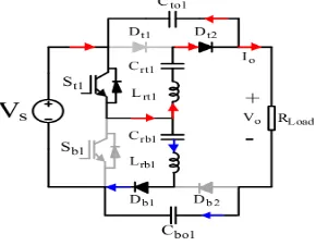
To understand the operational principle, the MRCC voltage tripler converter is selected as the topology under analysis. Fig. 5.5 shows the MRCC voltage tripler converter based on an SL module and a DS module. The MRCC converter consists of an SL-based module indicated by a red-colored box and an input module, as shown in Fig. 5.5. The MRCC voltage tripler can also be realized with a DS-based module represented by a blue-colored box and an output module (see Fig. 5.6).
Fig: 5.5. Structure of MRCC voltage Tripler
converter with SL-based module
converter with DS-based module
Therefore, both SL- and DS-based configurations have the same circuit for the voltage tripler converter. The active switches, Sb1 and St1, are controlled complementarily with a same duty cycle to minimize the conduction losses for the power devices and passive components 19. To simplify the analysis, the following assumptions are made:
1. All the switches, diodes, capacitors, and inductors are ideal;
2. The output capacitors, Cto1 and Cbo1, are large enough to be considered as voltage sources;
3. Two resonant inductors, Lrt1 and Lrb1, have the same inductances;
4. The resonant capacitors, Crt1 and Crb1, have identical values;
5. Vs is an ideal DC voltage source and the load is modelled by a pure resistor (Rload); and
6. The switching frequency is less than the resonant frequency to set aside enough dead time for two main switches and achieve a
zero-current switching (ZCS).
Therefore, the short time interval t1-t2 and t3-t4 are defined as the dead times between active switches to avoid a short circuit in each module.
1) State I t0-t1 Fig. 5.7
In the beginning of this mode (t = t0), the bottom switch, Sb1, is ON, whereas St1 is OFF in the top cell. The charging current flows through Dt1 and Sb1, as shown in Fig. 5.7. Therefore, Crt1 is charged by Vs, whereas Crb1 is discharged to Cto1 (Crb1 was previously charged at the input voltage level in Mode III) through the resonant loops (see Fig. 5.10 (f)). The energy of Rload is supplied by Cto1 and Crb1. At t = t1, Sb1 can be OFF under the zero-current condition (see Fig. 5.10(d)). The state equations of operating State I are
5.1
5.2
By ignoring the impact of the short times, t1 < t < t2 and t3 < t < t4, it can be assumed that t0 = 0, t1 = t2 « Ts /2, and t3 = t4 « Ts . The initial conditions of (5.1) and (5.2) are
and IL(0)=0 . Therefore, solving (5.1) and (5.2) gives the following:
5.3
5.4
The state equations of the operating State I for the resonant capacitor and inductor in the bottom cell can be expressed as
5.6
5.7
5.8
5.9 Equations (5.8) and (5.9) show that capacitor Crb1 is discharged in this mode (see Fig. 5.10(f)).
Fig: 5.7. Operating circuits in stages: Stage I t0—t1
2) State II t1-t2 Fig. 5.8
In this state, all the switches are turned OFF. The diodes are reversed-biased and the resonances stop, as shown in Fig. 5.8(b). Therefore, the inductor currents become zero (see Fig. 5.10(c)).
The resonant capacitor voltages of Crt1 and Crb2 are unchanged. Cto is connected in series to Cbo and both are discharged to the load terminal.
Fig: 5.8. Operating circuits in stages: Stage II t1—t2
3) State III t2-t3 Fig. 5.9
Fig: 5.9. Operating circuits in stages: Stage III t2—t3
Fig. 5.10(e) shows that the current through St1, is increased by a soft-switching operation with a half-cycle resonant shape. In this state, Crb1 is charged, whereas Crt1 is discharged through two resonant loops, as shown in Fig. 5.10. At time t3, St1 becomes OFF under the zero-current condition. This process can also be described mathematically as follows:
5.10
5.11
5.12
5.13
Therefore, in this state, the capacitor voltages and inductor currents can be obtained as follows
5.14
5.15
5.16
Fig: 5.10. Key current and voltage waveforms of the MRCC voltage Tripler converter.
It can be clearly observed from theoretical analysis and the operating principle of the MRCC converter that all the power devices and passive components have the same voltage and current stresses in this circuit.
4) State IV t3-t4 Fig. 5.8
The operation of this state is similar to that of State II.
5.3 Operating Principles of the 2n+1 level Cascaded SL- and DS-based Configurations
With the same principle, Figs. 5.11 to 5.14 show the 2n+1 level cascaded SL- and DS-based topologies, respectively. Note that n is an even number in Fig. 5.13 and 5.14.
5.3.1 Cascaded SL-based configuration
State I Fig. 5.11: During the period of t0 to t1, the bottom switch Sb is ON, whereas St is OFF. In each top cell, the diodes Dti1s (i=1, 2, ..., n) are forward-biased by Vs and Ctois. Therefore, Crtis are charged by Vs and Ctois (i=1, 2, ..., n-1), as shown in Fig. 7(a). In this state, Cton is discharged to the load. In contrast, in the bottom cells, Crbis are discharged to the output capacitors, Cbois. For the general 2n+1 level cascaded SL-based topology, the currents through the top and bottom capacitors are
5.18
5.19
5.20
Fig: 5.11. Operation states of the 2n+1 level cascaded SL-based topology State – I
Fig: 5.12. Operation states of the 2n+1 level cascaded SL-based topology State – III
State III Fig. 5.9: State III begins when the top switch St is in the ON-state and Sb is in the OFF-state at t0. The top diodes Dti2s
and bottom diodes Dbi1s are forward-biased, as shown in Fig. 7(b). In the bottom cells, Crbis are charged by Vs and Cbois (i=1,
2, ..., n-1), whereas Crtis are discharged to Ctois. As a result, the voltages of Crbis are equal to i times the input voltage level.
5.3.2 Cascaded DS-based configuration
Fig: 5.13. Operation states of the 2n+1 level cascaded DS-based topology State I
State I Fig. 5.13: At t = t0, Sbi (i=1, 3, ... n-1) and Sti (i=2, 4, ..., n) are turned ON, whereas Sbi (i=even) and Sti (i=odd) are OFF
in the top and bottom cells. Therefore, in the top and bottom cells, the odd numbered Crtis and even numbered Crbis are charged
by Vs, Crtis (i=2, 4,..., n), and Crbis (i=1, 3, .,., n-1). In this state, the output capacitor Cto is charged by Crtn, whereas Cbo is
discharged to the load, as shown in Fig. 5.13.
State III Fig.5.14: During this time interval, Sbis (i=1, 3, .,., n-1) and Stis (i=2, 4, ..., n) are OFF, whereas Sbis (for i even)
and Stis (for i odd) are ON. Therefore, in the top cells, Crtis (i=1, 3 .,., n-1) are discharged to Crtis (i=2, 4, ..., n). On the other
6.0
Simulation & Results
Fig: 6.1. MATLAB Based Simulation model of circuit under analysis
Voltage
--
-
--
Time ---
Voltage
--
-
--
Time ---
Fig: 6.3. Voltage Across Cb0 in Volts
Fig: 6.4. Voltage Across Ct0 in Volts
Fig: 6.6. Current through Lr1 in Amps
Fig: 6.8. Voltage across DC Filter in Volts
Bibliography
[1]. L. Wang and M. S. N. Thi, "Stability analysis of
four PMSG-based offshore wind farms fed to an
SG-based power system through an LCC-HVDC
Link," IEEE Trans. Ind. Electron., vol. 60, no. 6,
pp. 2392-2400, Jun. 2013.
[2]. T. Kawaguchi, T. Sakazaki, T. Isobe, and R.
Shimada, "Offshore wind farm configuration using
diode rectifier with MERS in current link
topology," IEEE Trans. Ind. Electron., vol. 60, no.
7, pp. 2930—2937, Jul. 2013.
[3]. M. A. Parker, L. Ran, and S. J. Finney,
"Distributed control of a fault-tolerant modular
multilevel inverter for direct-drive wind turbine
grid interfacing," IEEE Trans. Ind. Electron., vol.
60, no. 2, pp. 509-522, Feb. 2013.
[4]. A. Garces and M. Molinas, "A study of efficiency
in a reduced matrix converter for offshore wind
farms," IEEE Trans. Ind. Electron., vol. 59, no. 1,
pp. 184-193, Jan. 2012.
[5]. M. Liserre, R. Cardenas, M. Molinas, and J.
Rodriguez, "Overview of multi-MW wind turbines
and wind parks," IEEE Trans. Ind. Electron.,vol.
58, no. 4, pp. 1081-1096, Apr. 2011.
[6]. A. Parastar and J. K. Seok, "High-power-density
power conversion systems for HVDC-connected
offshore wind farms," J. Power Electron., vol. 13,
no. 5, pp. 746-756, Sep. 2013.
[7]. S. P. Engel, N. soltau, H. Stagge, and R. W. De
Doncker, "Dynamic and balanced control of
three-phase high-power dual-active bridge DC/DC
converters in DC-grid applications," IEEE Trans.
Power Electron., vol. 28, no. 4, pp. 1880-1889,
Dec. 2012.
[8]. N. Denniston, A. Massoud, S. Ahmed, and P.
Enjeti, "Multiple-module high-gain high-voltage
DC—DC transformers for offshore wind energy
systems," IEEE Trans. Ind. Electron., vol. 58, no. 5,
pp. 1877-1886, May 2011.
[9]. S. Gjerde, P. K. Olsen, K. Ljokelsoy, and T.
Undeland, "Control and fault handling in a modular
series connected converter for a transformerless
100 kV low weight offshore wind turbine," IEEE
Trans. Ind. Appl., vol.50, no. 2, pp. 1094-1105,