ISSN (Print) : 2320 – 3765 ISSN (Online): 2278 – 8875
I
nternational
J
ournal of
A
dvanced
R
esearch in
E
lectrical,
E
lectronics and
I
nstrumentation
E
ngineering
(An ISO 3297: 2007 Certified Organization)
Vol. 5, Issue 7, July 2016
Design of Parallel in Parallel out Shift Register
using Clocked Pass Transistor Logic
K.Chandra Sekhar1, S.Suresh2, P.V.K.Durga Prasad3, M.Loknath4, P.Pydi Reddy5
Assistant Professor, Dept. of ECE, RAGHU Institute of Technology, Visakhapatnam, Andhra Pradesh, India1
Assistant Professor, Dept. of ECE, RAGHU Institute of Technology, Visakhapatnam, Andhra Pradesh, India2
Associate Professor, Dept. of ECE, RAGHU Institute of Technology, Visakhapatnam, Andhra Pradesh, India3
Associate Professor, Dept. of ECE, RAGHU Institute of Technology, Visakhapatnam, Andhra Pradesh, India4
Assistant Professor, Dept. of ECE, RAGHU Institute of Technology, Visakhapatnam, Andhra Pradesh, India5
ABSTRACT: The major Power consuming component in most of the VLSI Circuit is Clock System. It consumes almost half of the total system power. It is necessary to reduce the power consumption because power budget is limited on portable digital circuits. In this paper, a new Low Power Clocked Pass Transistor Flip-Flop is proposed, which will considerably reduce the number of transistors in the discharging path and also reduces the capacity of the clock load by minimizing number of clocked transistors leading to reduction in clocking power which will improve the overall power consumption. Proposed reduced clock power flip flop is compared with conventional flip flops. Simulations are done using Microwind & Tanner software tools.
KEY WORDS: Flip-Flop; Low Power Clocking System; Pass transistors; Tanner; Micro-wind.
I. INTRODUCTION
Flip-Flops are extremely important circuit elements in all VLSI circuits. They are not only responsible for the correct timing, functionality and performance of the chip[1], but are also responsible for other clock distribution networks which consume a significant portion of the total power of the circuit. It is estimated that the power consumption of the clock system, which consists of clock distribution networks and storage elements, is as high as 20%–45% of the total system power. Moreover, flip-flops have a large impact on circuit speed. The performance of the Flip-Flop is an important element that determines the performance of the entire circuit.
ISSN (Print) : 2320 – 3765 ISSN (Online): 2278 – 8875
I
nternational
J
ournal of
A
dvanced
R
esearch in
E
lectrical,
E
lectronics and
I
nstrumentation
E
ngineering
(An ISO 3297: 2007 Certified Organization)
Vol. 5, Issue 7, July 2016
II. CONDITIONAL DATA MAPPING D FLIP-FLOP
Fig 1. Conditional Data Mapping Flip flop Design
Conditional Data Mapping Flip Flop (CDMFF) [3] used only 7 clocked transistors, resulting in about 50% reduction in the number of clocked transistors. The Fig.1 shows the Conditional Data Mapping Flip Flop Design. There is redundant clocking capacitance in CDMFF. When data remains 0 or 1, the pre-charging transistors, P1 and P2, keep switching without useful computation, resulting in redundant clocking. Clearly, it is necessary to reduce redundant power consumption here. Further, CDMFF has a floating node on critical path because its first stage is dynamic. When clock signal CLK transits from 0 to 1, CLKDB will remain 1 for a short period of time, which produces an implicit pulse window for evaluation. During that window, both P1, P2 are off. In addition, if D transits from 0 to 1, the pull down network will be disconnected by N3 using data mapping scheme (N6 turns off N3); If D is 0, the pull down network is disconnected from GND. Hence internal node X is not connected with Vdd or GND. During pulse windows, it is essentially floating periodically. With feature size shrinking, dynamic node is more prone to noise interruption because of the un-driven dynamic node. If a nearby noise discharges the node X, PMOS transistor P3 will be partially on, and a glitch will appear on output node Q. In a nano scale circuit, a glitch not only consumes power but could propagate to the next stage which makes the system more vulnerable to noise. Hence, CDMFF could not be used in noise intensive environment.
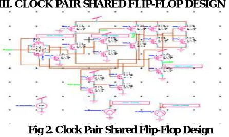
III. CLOCK PAIR SHARED FLIP-FLOP DESIGN
Fig 2. Clock Pair Shared Flip-Flop Design
ISSN (Print) : 2320 – 3765 ISSN (Online): 2278 – 8875
I
nternational
J
ournal of
A
dvanced
R
esearch in
E
lectrical,
E
lectronics and
I
nstrumentation
E
ngineering
(An ISO 3297: 2007 Certified Organization)
Vol. 5, Issue 7, July 2016
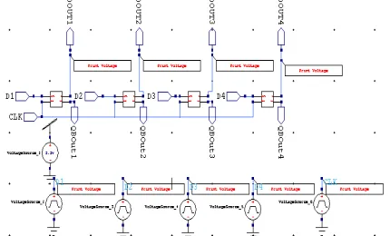
IV. PROPOSED LOW POWER CLOCKED PASS TRANSISTOR FLIP-FLOP DESIGN
Fig 3. Proposed Low Power Clocked Pass Transistor Flip-Flop
Proposed Low power Clocked Pass Transistor Flip-Flop is Designed [5-9] by using Pass Transistor Logic family, In this design only one clocking transistor is used so that it will consume less power in the clock network of the Flip flop. When clock signal CLK transits from 1 to 0, P1 is conducting then node X is precharged and Q is’0’, QB is ‘1’, at that time Data 0 or 1. When clock signal CLK transits from 0 to 1, P1 is not conducting then node X is discharged and Q is’1’, QB is ‘0’, at that time Data ‘1’.By using the proposed flip flop, power consumption and area required are reduced compared to other conventional flip flops, and also delay factor is reduced due to the reduced number of transistors. Therefore, the low power flip flop can be used in design sequential circuit when compared to other flip-flop designs for low power and area requirements.
V.SHIFT REGISTERS
Shift registers are a type of sequential logic circuit, mainly for storage of digital data. They are a group of flip-flops connected in a chain so that the output from one flip-flop becomes the input of the next flip-flop. Most of the registers possess no characteristic internal sequence of states. All flip-flop is driven by a common clock.The storage capacity of a register is the total number of bits (1 or 0) of digital data it can retain. Each stage (flip flop) in a shift register represents one bit of storage capacity. Therefore the number of stages in a register determines its storage capacity.
B
. PARALLEL IN PARALLEL OUT SHIFT REGISTERFor parallel in parallel out shift registers, all data bits appear on the parallel outputs immediately following the simultaneous entry of the data bits.
ISSN (Print) : 2320 – 3765 ISSN (Online): 2278 – 8875
I
nternational
J
ournal of
A
dvanced
R
esearch in
E
lectrical,
E
lectronics and
I
nstrumentation
E
ngineering
(An ISO 3297: 2007 Certified Organization)
Vol. 5, Issue 7, July 2016
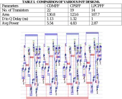
VI.SIMULATION RESULTS
To evaluate the performance, Shift Registers discussed in this paper are designed using 90-nm CMOS technology. All simulations are carried out using MICROWIND simulation tool at nominal conditions with 1GHz frequency range. Flip-Flop based Parallel in Parallel out Shift Register layout design is shown in Figure 7. The Simulation results are Shown in Figure 5 and Figure 6. The Comparison tables are shown in Table 1 , Table 2.
Fig.5 . Power consumed by LPCPFF. Fig 6. Power consumed by PIPO Shift Register using LPCPFF
TABLE I. COMPARISON OF VARIOUS P-FF DESIGNS.
Parameters
CDMFF
CPSFF
LPCPFF
No. of Transistors
22
19
14
Area
130.8
123.6
107.7
D to Q Delay (ns)
1.13
1.32
1
ISSN (Print) : 2320 – 3765 ISSN (Online): 2278 – 8875
I
nternational
J
ournal of
A
dvanced
R
esearch in
E
lectrical,
E
lectronics and
I
nstrumentation
E
ngineering
(An ISO 3297: 2007 Certified Organization)
Vol. 5, Issue 7, July 2016
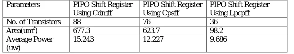
Table 2. Comparison of various Parallel in Parallel out Shift Register designs.
Parameters
PIPO Shift Register
Using Cdmff
PIPO Shift Register
Using Cpsff
PIPO Shift Register
Using Lpcpff
No. of Transistors
88
76
36
Area(um
2)
677.3
623.7
98.2
Average Power
(uw)
15.243
12.227
9.686
VII. CONCLUSION
The Low Power Clocked Pass Transistor Flip Flop (LPCPTFF) design in the clocked load resulting in reduction in number of Transistors and Power consumption and Delay. LPCPFF uses less number of transistors compared to CDMFF and CPSFF resulting in reduced area and delay. Power consumption in LPCPFF is reduced by 51.8% compared to CDMFF and 59.4% compared to CPSFF. From the results it is evident that LPCPFF is more power efficient, speed and occupies less area. This flip flop is very much useful in computer systems and in SOC applications.
REFERENCES
[1] Peiyi Zhao, Jason McNeely, Weidong Kuang, Nan Wang, and Zhongfeng Wang “Design of Sequential Elements for Low Power Clocking
System” IEEE Transactions on Very Large Scale Integration (VLSI) Systems, vol. 19, no. 5, May 2011
[2] Seyed E. Esmaeili, Asim J. Al-Kahlili, and Glenn E. R. Cowan “Low Swing Differential Conditional Capturing Flip-Flop for LC Resonant Clock Distribution Networks” IEEE Transactions on Very Large Scale Integration (VLSI) Systems, vol. 20, no. 8, aug 2012.
[3] C. K. Teh, M. Hamada, T. Fujita, H. Hara, N. Ikumi, and Y. Oowaki, “Conditional data mapping flip-flops for low-power and
high-performance systems,” IEEE Trans. Very Large Scale Integr. (VLSI), vol.14, no.12, Dec. 2006.
[4] B. Kong, S. Kim, and Y. Jun, “Conditional-capture flip-flop for statistical power reduction,” IEEE J. Solid-State Circuits, vol. 36, no. 8, pp.1263–1271, Aug. 2001.
[5] H. Kawaguchi and T. Sakurai, “A Reduced Clock-Wing Flip-Flop (RCSFF) for 63% power reduction,” IEEE Solid-State Circuits, vol.33, no.
5, pp. 807–811, May 1998.
[6] A. Chandrakasan, W. Bowhill, and F. Fox, “Design of High-Performance Microprocessor Circuits,” 1st ed. Piscataway, NJ: IEEE Press, 2001.
[7] J.Tschanz, S.Narendra, Z.P.Chen, S.Borkar, M.Sachdev, and V. De, “Comparative delay and energy of single edge-triggered & dual edge triggered pulsed flip-flops for high-performance microprocessors,” in Proc. ISPLED, Huntington Beach, CA, Aug. 2001, pp.207–212.
[8] P. Zhao, J. McNeely, P. Golconda, M. A. Bayoumi, W. D. Kuang, and B. Barcenas, “Low power clock branch sharing double-edge triggered
flip-flop,” IEEE Trans. Very Large Scale Integr. (VLSI) Syst., vol. 15, no. 3, pp. 338–345, Mar. 2007.
[9] C. L. Kim and S. Kang, “A low-swing clock double edge-triggeredflip-flop,” IEEE J. Solid-State Circuits, vol. 37, no. 5, pp. 648–652, May