c e-ISSN: 2348-6848, p- ISSN: 2348-795X Volume 3, Issue 01, January 2016
International Journal of Research (IJR)
Available at http://internationaljournalofresearch.org
Available online:http://internationaljournalofresearch.org/ P a g e | 509
A Eleven Level Grid Connected Transformer Less PV
Systems
T. Siva Rama Krishna & Mr. A. Suryanarayana Babu
PG Scholar Nova College Of Engineering And Technology Jangareddy Gudem , Department Of Electrical And Electronics Engineering , JNTUK Andhra Pradesh, India.
Nova College Of Engineering And Technology Jangareddy Gudem , Department Of Electrical And Electronics Engineering , JNTUK Andhra Pradesh, India.
ABSTRACT
This paper presents a single-phase transformer less grid-connected photovoltaic converter based on two cascaded full bridges with different dc-link voltages. The converter can synthesize up to eleven voltage levels with a single dc bus, since one of the full bridges is supplied by a flying capacitor. The multilevel output reduces harmonic distortion and electromagnetic interference. A suitable switching strategy is employed to regulate the flying-capacitor voltage, improve the efficiency (most devices switch at the grid frequency), and minimize the common-mode leakage current with the help of a novel dedicated circuit (transient circuit). Simulations and experiments confirm the feasibility and good performance of the proposed converter.
INTRODUCTION
When no transformer is used in a grid-connected photovoltaic (PV) system, a galvanic connection between the grid and the PV array exists. In these conditions, dangerous leakage currents (common-mode currents) can appear through the stray capacitance between the PV array and the ground. In order to avoid these leakage currents, different inverter topologies that generate no varying common-mode voltages, such as the half-bridge and the bipolar pulsewidth modulation (PWM) full-bridge topologies, have been proposed. The need of a high-input voltage represents an important drawback of the half-bridge. The bipolar PWM full bridge requires a lower input voltage but exhibits a low efficiency. This letter proposes a new high-efficiency topology that generates no varying common-mode
c e-ISSN: 2348-6848, p- ISSN: 2348-795X Volume 3, Issue 01, January 2016
International Journal of Research (IJR)
Available at http://internationaljournalofresearch.org
Available online:http://internationaljournalofresearch.org/ P a g e | 510
found in literature aiming at the reduction of the common-mode voltage harmonic content [5]–[7]. Once the grid frequency transformer is removed from a PV converter, the bulkiest wound and reactive components that remain are those that form the output filter used to clean the output voltage and current from high frequency switching components. Further reduction in cost and weight and improvement in efficiency can be achieved by reducing the filter size, and this is the goal of multilevel converters. Multilevel converters have been investigated for years [8], but only recently have the results of such researches found their way to commercial PV converters. Since they can synthesize the output voltages using more levels, multilevel converters outperform conventional two- and three-level converters in terms of harmonic distortion. Moreover, multilevel converters subdivide the input voltage among several power devices, allowing for the use of more efficient devices. Multilevel converters were initially employed in high-voltage industrial and power train applications. They were first introduced in renewable energy converters inside utility-scale plants, in which they are still largely employed [9]–[13]. Recently, they have found their way to residential-scale single-phase PV converters, where they currently represent a hot research topic [14]–[29]. Single-phase multilevel converters can be roughly divided into three categories based on design: neutral point clamped (NPC), cascaded full bridge (CFB), and custom.In NPC topologies, the electrical potential between the PV cells and the ground is fixed by connecting the neutral wire of the grid to a constant potential, resulting from a dc-link capacitive divider [15]. A huge advantage is that single-phase NPC converters are virtually immune from ground leakage currents, although the same is not true for three-phase NPC converters [12], [30]. A recent paper has proposed an interesting NPC design for exploiting next-generation devices such as super junction or Sic MOSFETs [16]. The main drawback of NPC designs, with respect to full bridge, is that they need twice the dc-link voltage. CFBs make for highly modular designs. Usually,
c e-ISSN: 2348-6848, p- ISSN: 2348-795X Volume 3, Issue 01, January 2016
International Journal of Research (IJR)
Available at http://internationaljournalofresearch.org
Available online:http://internationaljournalofresearch.org/ P a g e | 511
achieved using custom architectures. In fairness, it should be noted that two additional very low power switches and a line frequency switching device [transient circuit (TC)] were included in the final topology in order to reduce the ground leakage current. The custom converter proposed in [29] generates five levels with six switches but has no intrinsic boosting capability. In [25], Raiment eludes three dc-bus capacitors in series together with two bidirectional switches (diode bridge+ unidirectional switch) and an H-bridge to generate seven output levels; however, they give no explanations on how they keep the capacitor voltages balanced. In [27], five switches, four diodes, and two dc-bus capacitors in series are used to generate five levels with boosting capability. Again, no mention is made about how the capacitors are kept balanced. In PV applications, the PV field dc voltage is constantly changing due to variations of solar radiation and to the MPPT algorithm, but the output voltage has to be controlled regardless of the voltage ratio. This problem was studied in [34]–[36], measuring the separate full-bridge voltages and computing online the duty cycles needed to balance the different voltages, and analyzing also the power balance between the separate cells. A similar approach is followed in this paper. Moreover, the developed PWM strategy, in addition to controlling the flying capacitor voltage, with the help of the specific TC illustrated in Section IV, minimizes the ground leakage current. Finally, it
1. CFB with a flying capacitor.
is important to put in evidence that the proposed converter can work at any power factor as reported in Section III, while not all the alternative proposals can continuously supply reactive power [37], [38] The proposed topology was presented by the authors in a previous paper [39]. With respect to the previous work, this paper was rewritten and presents a better organization and a new set of simulation and experimental results with different setups. This paper is organized as follows: Section II presents the power converter topology and the PWM control strategy chosen in order to maximize the performance with the use of a low-cost digital signal processor (DSP). Section III describes the regulation of the flying capacitor used to supply the second full bridge of the CFB topology. Section IV describes the principle of operation of the additional components able to reduce the ground leakage current. Sections V and VI show the simulation and experimental results, whereas Section VII reports the concluding remarks.
MODELING OF PROPOSED THEORY
ELEVEN-LEVELCONVERTER AND
PWM CONTROLSTRATEGY
c e-ISSN: 2348-6848, p- ISSN: 2348-795X Volume 3, Issue 01, January 2016
International Journal of Research (IJR)
Available at http://internationaljournalofresearch.org
Available online:http://internationaljournalofresearch.org/ P a g e | 512
bipolar transistors (IGBTs) with fast anti n parallel diodes are required in the legs where high-frequency hard switching commutations occur. In grid-connected operation, one full-bridge leg is directly connected to the grid neutral wire, where as the phase wire is connected to the converter through an LC filter.
As it will be described and justified in the following section, flying-capacitor voltageVfc is kept lower, at steady state, than dc-link voltageVDC. Accordingly, the full bridge supplied by the dc link is called the high-voltage full bridge (HVFB), whereas the one with the flying capacitor is the low-voltage full-bridge (LVFB).
The CFB topology allows certain degrees of freedom in the control, so that different PWM schemes can be considered; however, the chosen solution needs to satisfy the following requirements.
1) Most commutations must take place in the LVFB to limit the switching losses.
2) The neutral-connected leg of the HVFB needs to switch at grid frequency to reduce the ground leakage current.
3) The redundant states of the converter must be properly used to control the flying-capacitor voltage.
4) The driving signals must be obtained from a single carrier for a low-cost DSP to be used as a controller.
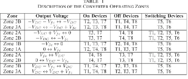
The switching pattern described in Table I was developed starting from the above requirements. Requirement 2), in particular, is due to the aforementioned parasitic capacitive coupling between the PV panels and their frames, usually connected to the earth. Capacitive coupling renders the common-mode current inversely proportional to the switching frequency of the neutral-connected leg. The converter can operate in different output
voltage zones, where the output voltage switches between two specific levels. The operating zone boundaries vary according to the dc-link and flying-capacitor voltages, and adjacent zones can overlap (see Fig. 2). In zones labeled A, the contribution of the flying-capacitor voltage to the converter output voltage is positive, whereas it is negative in B zones. Constructive cascading of the two full bridges can, therefore, result in limited output voltage boosting. Depending on theft/VDCratio, one of the (a) or (b) situations in Fig. 2 can ensue; nevertheless, the operation of the converter does not differ much in the two cases. If two overlapping operating zones can supply the same output voltage, the operating zone to be used is determined taking into account the regulation of Vic, as will be described in Section III. As mentioned in the introduction, the duty cycles are calculated on-line by a simple equation, similarly to the approach presented in [34]. The switching pattern depends on the instantaneous fundamental component of output voltage ∗ outland on the measured values of Vic and VDC.
Fig. 2. Operating zones under differentVfc ranges. (a) Vic <0.5VDC. (b)Vic >0.5VDC.
c e-ISSN: 2348-6848, p- ISSN: 2348-795X Volume 3, Issue 01, January 2016
International Journal of Research (IJR)
Available at http://internationaljournalofresearch.org
Available online:http://internationaljournalofresearch.org/ P a g e | 513
the whole HVFB (see Fig. 2). Since the voltage regulation of the flying capacitor takes place in zone 2, the zone-2 behavior is more articulated and will be described in detail in the following section.
FLYI NG-CAPACITOR VOLTAGE
REGULATION
Since the main task facing a grid-connected PV converter is the transfer of active power to the electrical grid, controlling the voltage of the flying capacitor is critical.
Flying-capacitor voltageVfc is regulated by suitably choosing the operating zone of the converter depending on the instantaneous output voltage request. Depending on the operating zone of the converter (see Fig. 2), Vfc can be added to
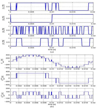
Fig. 3. Theoretical waveforms of the proposed converter. (a) PWM switching patterns. (b) Output voltages.
(A zones) or subtracted from (B zones) the HVFB output voltage, charging or discharging the flying capacitor. In particular, considering a positive value of the current injected into the grid, the flying capacitor is discharged in A zones and charged in B zones. Since a number of redundant switch configurations can be used to synthesize the same output voltage waveform, it is possible to control the voltage of the flying capacitor, forcing the converter to operate more in a zones when the
flying-capacitor voltage is higher than a reference value or more in B zones when it is lower than a reference value. Similar considerations hold in case of a negative injected grid current. In each case, some commutations between nonadjacent output levels must inevitably occur (level skipping), with the drawback of a certain increase in the output current ripple. The voltage control of the flying capacitor (which determines the zone-A or zone-B operation) is realized by a simple hysteresis control.
Fig. 4. Converter configurations for the regulation of the flying capacitor. (a) Flying-capacitor charge. (b) Flying-capacitor discharge.
c e-ISSN: 2348-6848, p- ISSN: 2348-795X Volume 3, Issue 01, January 2016
International Journal of Research (IJR)
Available at http://internationaljournalofresearch.org
Available online:http://internationaljournalofresearch.org/ P a g e | 514
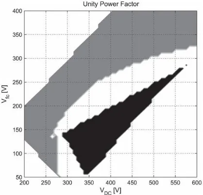
strategy, it is important that the converter is able to work in any [VDC, Vfc] condition. While the distortion of the output voltage is minimized through the on-line duty cycle computation, it is important to assess the capability of the converter to regulate the flying-capacitor voltage under different operating conditions. The ability to control the flying-capacitor voltage through the proposed PWM strategy has been studied in simulation by determining the average flying-capacitor current under a large span ofVDCandVfc values. In the simulations, grid voltage grid is sinusoidal with amplitude of 230 √2V; however, the same results hold even for different voltages if the ratio Grid/VDC remains constant. The results in the case of unity power factor are summarized in Fig. 5. The white area covers the range over which Vic is fully controllable, whereas it cannot be controlled in the gray and black regions. In particular, in the black region, Vfc cannot be decreased, whereas in the gray region, it cannot be increased.
Fig. 5. Flying-capacitor voltage regulation regions.
Therefore, the white region located between the gray and black ones is a stable and safe operating area for the converter. Even ifVfc was not actively controlled, it would be constrained inside the white region, ensuring that the flying capacitor cannot be over charged nor completely discharged. The
results are not affected by the amplitude of the grid current. Nevertheless, the power factor affects the results: a lower power factor determines widening of the controllable area. When the converter supplies only reactive power, Vfc is controllable in the entire [VDC, Vfc] domain.
APPLICATION TO TRANSFORMERLESS PV CONVERTERS—TC
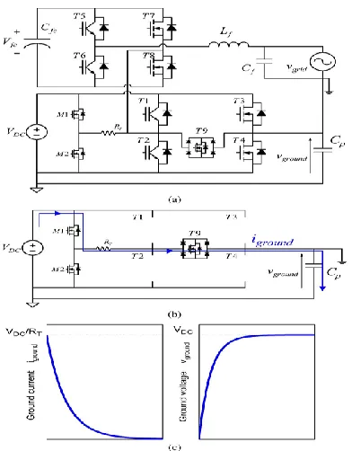
A particular feature of the commutation pattern of Table I am that T3 and T4 switch at grid frequency, commutating at every zero crossing of grid. If the zero crossing with a negative derivative is considered, T4 opens and T3 closes, changing the neutral wire voltage (and thus the voltage across the parasitic capacitance of the PV field) from zero told. For this reason, the commutation can cause a large surge of leakage current that can decrease the power quality and damage the PV modules. A proper TC was designed to decrease these surge currents. Fig. 6(a) shows the proposed converter topology; it is constituted of the two-cell CFB described in Fig. 1 with the addition of the TC components. In order to better understand the behavior of the TC, the distributed parasitic capacitance of the PV source was modeled with a simple equivalent parasitic capacitance, i.e., Cp, connected between the negative pole of the dc link and the ground.
c e-ISSN: 2348-6848, p- ISSN: 2348-795X Volume 3, Issue 01, January 2016
International Journal of Research (IJR)
Available at http://internationaljournalofresearch.org
Available online:http://internationaljournalofresearch.org/ P a g e | 515
Fig. 6. Ground leakage current limitation circuit topology and behavior. (a) TC topology. (b) TC operation. (c) TC waveforms.
Capacitorvgroundstays constant [see Fig. 6(b)]. At this point, one of M1 and M2 is turned on (M1 if the slope of the zero crossing is negative and M2 if positive). So doing, Cpis charged throughRTwith a first-order transient [see Fig. 6(c)], limiting the current surge.
Whereas the TC introduces additional components, they can be selected with current ratings much lower than the devices of the CFB. Moreover, the power loss due to the added resistor is negligible. Estimating the energy lost charging and discharging a capacitorCpto VDCaveraged over a line periodTbyPtc = Cap 2 DC/T, with Cp= 200nF add= 300V, a dissipation of about 1 W is obtained. The operation of the TC is not affected by the power factor because in grid-connected operation, the output voltage is always very close to the grid voltage. The correct operation of the TC requires the grid voltage instantaneous angle that can be obtained with a phase-locked loop (PLL) fed by the grid voltage [40].
Fig. 7. Simulation results withed= 300V.
SIMULATIONRESULTS
The proposed converter and PWM were extensively simulated under MATLAB/Semolina, using the PLECS toolbox. The simulations cover a large range of active and reactive power injected into the grid, dc-link voltage, and equivalent PV parasitic capacitance.
A dc-link voltageVDC= 300V was used in the simulations, unless otherwise specified. The grid was represented by a sinusoidal voltage source at 50 Hz of amplitude grid= 230V. The output filter was composed of a capacitors =1μF and an inductor Lf =1.5mH. An additional inductor Lurid=40μH represented the total distributed grid inductance. The PWM frequency was fess=20 kHz, and the flying capacitor had a capacitance of CFC = 500μF. The surge limiting resistance RT was selected as 1.5 co. The current injected into the grid was regulated through a proportional-integral regulator plus feed forward at I grid=8.5Arms. As stated above, the injection of both active and reactive power was simulated; however, the switches being ideal and the commutations instantaneous, performance did not depend on the power factor. For this reason, only the unity power factor simulation results are reported. In the simulations, the grid voltage angle information is available; hence, a PLL was not employed.
c e-ISSN: 2348-6848, p- ISSN: 2348-795X Volume 3, Issue 01, January 2016
International Journal of Research (IJR)
Available at http://internationaljournalofresearch.org
Available online:http://internationaljournalofresearch.org/ P a g e | 516
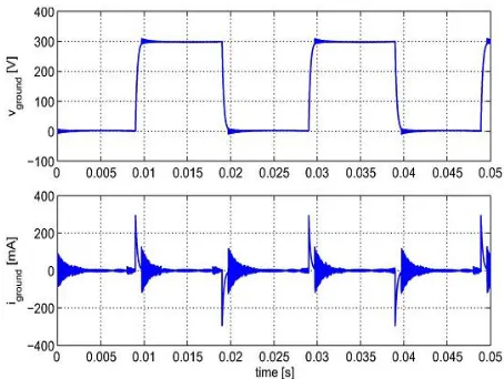
Fig. 8 shows the performance of the TC with a parasitic capacitance of the PV field of Cp= 200nF.
The ground leakage current results aground=30mA rms. Please note that
Fig. 8. TC behavior with a 200 no parasitic capacitor.
Only a common-mode inductor of 1 my was employed in this setup. The ground leakage current could be further reduced by a more accurate design of the common-mode filter.
In order to obtain further indications about the regulation of the flying-capacitor voltage, Fig. 9 reports the result of a step variation off from 150 to 190 V (inside the controllable region in Fig. 5) occurring at time 0.1 s. As it can be seen, the average value of Vic rapidly (in about 25 ms) rises to the reference value without any overshoot.
CONCLUSION
This paper has proposed a novel eleven-level grid-connected transformer less PV converter based on a CFB topology with two full bridges, one of which is supplied by a floating capacitor. A suitable PWM strategy was developed in order to improve efficiency (most power devices commutate at low frequency) and, with the help of a specific TC, minimize the ground leakage current. The proposed PWM strategy can regulate the voltage across the flying capacitor. Simulations were performed to assess the ability to regulate the flying-capacitor voltage in a wide range of
operating conditions. Extensive simulations and experiments confirm the results of the theoretical analysis and show the good performance of the converter as far as ground leakage current and harmonic distortion are concerned. Despite the use of traditional power devices for the laboratory prototype, the experimentally measured efficiency was fairly good. The proposed converter can continuously operate at arbitrary power factors, has limited boosting capability, and can produce eleven output voltage levels with 11 power switches, of which three are low power switches for the TC and only four needs to be controlled by PWM.
REFERENCES
[1] G. Butcher, L. Consoling, and E. Lorenzani, “Active filter for the removal of the dc current component for single-phase power lines,”IEEE Trans. Ind. Electron., vol. 60, no. 10, pp. 4403– 4414, Oct. 2013.
[2] G. Butcher and E. Lorenzani, “Detection method of the dc bias in distribution power transformers,” IEEE Trans. Ind. Electron., vol. 60, no. 8, pp. 3539–3549, Aug. 2013.
[3] H. Xiao and S. Xian, “Leakage current analytical model and application in single-phase transformer less photovoltaic grid-connected inverter,”IEEE Trans. Electromagnet. Compact. vol. 52, no. 4, pp. 902–913, Nov. 2010.
[4] O. Lopez, F. Freaked, A. Yaps, P. Fernandez-Comes, J. Malvern, R. Teodorescu, and J. Doval-Gandoy, “Eliminating ground current in a transformer less photovoltaic application,” IEEE Trans. Energy Converse., vol. 25, no. 1, pp. 140– 147, Mar. 2010.
c e-ISSN: 2348-6848, p- ISSN: 2348-795X Volume 3, Issue 01, January 2016
International Journal of Research (IJR)
Available at http://internationaljournalofresearch.org
Available online:http://internationaljournalofresearch.org/ P a g e | 517
[6] D. Barrater, G. Butcher, A. Crinite, G. Franceschini, and E. Lorenzani, “Unipolar PWM strategy for transformer less PV grid-connected converters,”IEEE Trans. Energy Convers., vol. 27, no. 4, pp. 835–843, Dec. 2012.
[7] T. Kerekes, R. Teodorescu, P. Rodridguez, G. Vazquez, and E. Aldabas, “A new high-efficiency single-phase transformerless PV inverter topology,” IEEE Trans. Ind. Electron., vol. 58, no. 1, pp. 184–191, Jan. 2011.
[8] S. Kouro, M. Malinowski, K. Gopakumar, J. Pou, L. Tranquillo, B. Wu, J. Rodriguez, M. P. Andres, and J. Leon, “Recent advances and industrial applications of multilevel converters,”IEEE Trans. Ind. Electron., vol. 57, No. 8, pp. 2553–2580, Aug. 2010.
[9] Y. Due, B. Gee, and F. Z. Pang, “Reliability, efficiency, and cost comparisons of mw-scale photovoltaic inverters,” import. IEEE ECCE, Raleigh, NC, USA, Sep. 2012, pp. 1627–1634.
[10] C. Townsend, T. Summers, and R. Betz, “Control and modulation scheme for a cascaded H-bridge multi-level converter in large scale photovoltaic systems,” import. IEEE ECCE, Raleigh, NC, USA, Sep. 2012, pp. 3707–3714.
[11] S. Essakiappan, H. Krishnamurthy, P. Emetic, R. Blog, and S. Ahmed, “Independent control of series connected utility scale multilevel photovoltaic inverters,” import. IEEE ECCE, Raleigh, NC, USA, Sep. 2012, pp. 1760–1766.
[12] G. Konstantin, S. Pulikanti, M. Ciobotaru, V. Agilities, and K. Muttaqi, “The seven-level flying capacitor based ANPC converter for grid integration of utility-scale PV systems,” in Proc. IEEE PEDG, Aalborg, Denmark, Jun. 2012, pp. 592–597.
[13] G. Brando, A. Dannie, A. Del Pizza, and R. Rizzo, “A high performance control technique of power electronic transformers in medium voltage
grid-connected PV plants,” import. ICEM, Rome, Italy, Sep. 2010, vol. 2, pp. 1–6.
[14] G. Butcher, E. Lorenzani, and G. Franceschini, “A five-level single-phase grid-connected converter for renewable distributed systems,”IEEE Trans. Ind. Electron., vol. 60, no. 3, pp. 906–918, Mar. 2013.
[15] Y. Kashihara and J. Itch, “The performance of the multilevel converter topologies for PV inverter,” in Proc. CIPS, Beijing, China, Mar. 2012, pp. 1–6.
[16] Y. Noge and J. Itch, “Multi-level inverter with H-bridge clamp circuit for single-phase three-wire grid connection suitable for super-junction–Sic MOSFET,” import. IPEMC, Harbin, China, Jun. 2012, vol. 2, pp. 88–93.
[17] C. Cacti, F. Canetti, and P. Sian, “A multilevel inverter for photovoltaic systems with fuzzy logic control,”IEEE Trans. Ind. Electron., vol. 57, no. 12, pp. 4115–4125, Dec. 2010.
[18] I. Abdulla, J. Corday, and L. Zhang, “Multilevel dc-link inverter and control algorithm to overcome the PV partial shading,” IEEE Trans. Power Electron., vol. 28, no. 1, pp. 14–18, Jan. 2013.
[19] J. Chavarria, D. Biel, F. Guenon, C. Meza, and J. Negron, “Energy balance control of PV cascaded multilevel grid-connected inverters under level-shifted and phase-shifted PWMS,”IEEE Trans. Ind. Electron., vol. 60, no. 1, pp. 98–111, Jan. 2013.