Available Online atwww.ijcsmc.com
International Journal of Computer Science and Mobile Computing
A Monthly Journal of Computer Science and Information Technology
ISSN 2320–088X
IJCSMC, Vol. 2, Issue. 11, November 2013, pg.203 – 209
RESEARCH ARTICLE
IMPLEMENTATION FOR 3-D DISCRETE
WAVELET TRANSFORM BY USING
EFFICIENT ARCHITECTURE
Ch. Madhuri, T. Guru Charan (Associate Professor), Y. Shekar (Asst-Professor)
Ganapathy College of Engineering, Warangal, Andhra Pradesh, India
Ganapathy College of Engineering, Warangal, Andhra Pradesh, India
Balaji Institute of Engineering and Science, Warangal, Andhra Pradesh, India
Email - [email protected], [email protected], [email protected]
Abstract- The digital data can be transformed using Discrete Wavelet Transform (DWT). The images need to be transformed without loosing of information. The Discrete Wavelet Transform (DWT) was based on time-scale representation, which provides efficient multi-resolution. The lifting based scheme (5, 3) (Here 5 Low Pass filter coefficients and the 3 High Pass filter coefficients) filter give lossless mode of information as per the JPEG 2000 Standard. The lifting based DWT are lower computational complexity and reduced
memory requirements. Since Conventional
convolution based DWT is area and power hungry which can be overcome by using the lifting based scheme.
The discrete wavelet transform (DWT) is being increasingly used for image coding. This is due to the fact that DWT supports features like progressive image transmission (by quality, by
resolution), ease of transformed image manipulation, region of interest coding, etc. DWT has traditionally been implemented by convolution. Such an implementation demands both a large number of computations and a large storage features that are not desirable for either high-speed or low-power applications. Recently, a lifting-based scheme that often requires far fewer computations has been proposed for the DWT. In this work, the design of Lossless 3-D DWT (Discrete Wavelet Transform) using Lifting Scheme Architecture will be modeled using the Verilog HDL and its functionality were verified using the Model sim tool and can be synthesized using the Xilinx tool.
I.INTRODUCTION
The fundamental idea behind wavelets is to analyze according to scale. Indeed, some researchers in the wavelet field feel that, by using wavelets, one is adopting a perspective in processing data. Wavelets are functions that satisfy certain mathematical requirements and are used in representing data or other functions. This idea is not new. Approximation using superposition of functions has existed since the early 1800's, when Joseph Fourier discovered that he could superpose sines and cosines to represent other functions. However, in wavelet analysis, the scale that we use to look at data plays a special role. Wavelet algorithms process data at different scales or resolutions.
Fourier Transform (FT) with its fast algorithms (FFT) is an important tool for analysis and processing of many natural signals. FT has certain limitations to characterize many natural signals,
which are non-stationary (e.g. speech). Though a time varying, overlapping window based FT namely STFT (Short Time FT) is well known for speech processing applications, a time-scale based Wavelet Transform is a powerful mathematical tool for non-stationary signals. Wavelet Transform uses a set of damped oscillating functions known as wavelet basis. WT in its continuous (analog) form is represented as CWT. CWT with various deterministic or non-deterministic bases is a more effective representation of signals for analysis as well as characterization. Continuous wavelet transform is powerful in
singularity detection. A discrete and fast
implementation of CWT (generally with real valued basis) is known as the standard DWT (Discrete Wavelet Transform).With standard DWT, signal has a same data size in transform domain and therefore it is a non-redundant transform. A very important property was Multi-resolution Analysis (MRA) allows DWT to view and process.
II.PROPOSEDARCHITECTURE
Working Principle
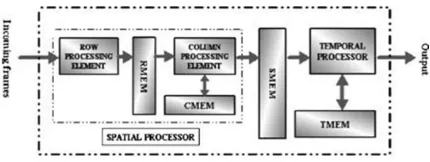
Fig. 1 presents the proposed scan-based 1 level 3-D wavelet transform architecture with a block level illustration of principal functional modules. Clearly from the figure, the proposed architecture does the spatial transform first, followed by its temporal counterpart. The following two parts in this section give a detailed view about hand-in-hand working of the different functional blocks to realize those two transform components.
Fig. 1, proposed architecture RMEM. Line buffers store row processed data CMEM, as well as intermediate results of column processing SMEM. Frame buffers store spatially transformed data TMEM, as well as intermediate results of temporal transform.
1) Spatial Transform: Scanned row-wise with double clock, the incoming frames are fed to the spatial processors (SP) which transform them two dimensionally with the help of two dedicated
With the previously mentioned double scanning, two pixels are fed into SP while two results emerge out of it in every clock cycle, which necessitate a total of (N2/2) cycles to complete the computation of each frame. If the frames have an even number of rows, both the processing elements run smoothly without any interruption during the skip from one frame to the next. However, for the frame having an odd number of rows, the CPE has to remain idle for N/2 cycles (corresponding to one row) at the beginning of each frame to get the first two rows processed. Importantly, in the second instance too, no extra clock cycles are spent by the SP to complete the computation of individual frame.
2) Temporal Transform: The transformed frames, to be decomposed subsequently in the temporal domain, are primarily stored in two dual port frame buffers of spatial Memory module (SMEM), as shown in Fig. 1. With two such initial frames already stored, and the third one approaching, the temporal processor (TP) starts computing the final transform component of 3-D-DWT. While at every cycle, two pixels of previous two frames are read out from SMEM buffers for the computation, the respective locations are utilized for the reposition of two incoming pixels of the current frame. Nevertheless, the computation necessitates more; one pixel of the third frame is to be read out again from memory at single clock rate, which can be fulfilled through the utilization of the second port of the dual-port RAMs. Thus, the temporal processing proceeds altogether while the RAM locations are refreshed in a
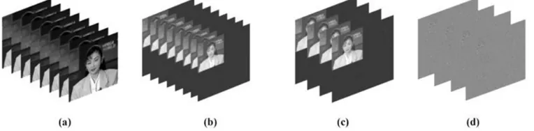
continuous manner and after passing a N2 clock cycles, the current phase of the computation is completed. Additionally, the SMEM buffers are totally filled up with the pixels of the third and fourth frames. In the very next cycle, the corresponding operations of the next phase start in a similar manner with the temporal processor getting busy with the computation of the third, fourth, and fifth frames. The details of the cyclic computation pattern for the temporal and column decompositions are discussed in Section III-C. To incorporate periodicity in the data flow associated with SMEM, efficient memory arrangement and addressing strategy are used. The details are furnished in Section III-E. Like the CPE, the temporal processor produces some temporary results during its operation, which are called back in later cycles repetitively and the temporal memory module (TMEM), which contains three frame buffers inside is used as a storage space for those results. Finally, a group of illustrated pictures is presented in Fig. 2 which helps in understanding the sequence of operations involved in the processing.
Provisions are open for multilevel transform with the current architecture. The simplest possible form will be cascading several 1 level architectures where the lll sub-band from one level is passed onto the next. The final output data set then needs to be synchronized or reordered according to the need of a specific encoder.
The following sections discuss the detailed design of principal working modules in the architecture
Fig. 2. Spatio-temporal wavelet decomposition with proposed architecture. (a) Original frame sequence. (b) After 1 level spatial transform. (c) Low pass frames after the temporal transform. (d) High pass frames after the temporal transform.
II.THEORETICAL FRAMEWORK
As the DWT intrinsically constitutes a pair of filtering operations, a unified representation of the polyphase matrix is introduced as follows:
P(z) =∏ h (z) g (z)
h (z) g (z) (1)
Thus, the transform is symbolized with the equation
(λ(z) γ(z)) = (x (z) z x (z))P(z) (2)
With λ (z) and γ (z) signifying the filtered
low pass and high pass parts of the input x (z).
The lifting scheme factorizes the polyphase representation into a cascade of upper and lower triangular matrices and a scaling matrix which subsequently return a set of linear algebraic equations in the time domain bringing forth the possibility of a pipelined processor.
For instance, the common Daubechies (9, 7) filter bank can be factorized as
P(z) = 1 α(1 + z )
0 1
1 0
β(1 + z) 1 1 γ(1 + z )
0 1
1 0
δ(1 + z) 1
ζ 0
0 (1 ζ) (3)
The related algebraic equations are
s = x (Splitting) d = x
d = d +α x(s + s ) (PredictP1) s = s + β x(d + d ) (Update U1)
d = d + γ x(s + s ) (PredictP2) s = s + δ x(d + d ) (UpdateU2)
s = ζ xs (ScalingS1) d = 1 ζ xd (ScalingS2)
where α = −1.586134342, β =
−0.05298011854, γ =0.8829110762, δ = 0.4435068522, and ζ = 1.149604398 [16], and also 0
≤i≤−1, L is the data length.
The critical path delay for the above lifting equations is 5Tm + 8Ta, where Tm and Ta denote the multiplier and adder delay. The primary reason behind this large delay is stacking of multipliers from the inputs to outputs. As a fruitful result, the processing speed increases significantly when the flipped equations are mapped into hardware.
Following the modification on SFG, the final equations for flipping are
s = x (Splitting) d = x
d = Axd + (s + s ) (PredictP1)
s = Bxs + (Update U1)
d = Cxd + (s + s )
2 (PredictP2)
s = Dxs + (UpdateU2)
s = K0xs (ScalingS1) d = K1xd (ScalingS2)
where A = (1/α) = −0.630463, B = (1/16αβ)
= 0.743750, C = (1/32βγ) = −0.668067, D = (1/4γδ) = 0.638443, K0 (64αβγδ) = 2.590697 and K1 = (32αβγ/δ) = 1.929981 (up to six fractional digits) and
also 0 ≤ i≤ L − 1, L is the data length .
To handle the truncation of the signals at
boundaries, mirror extension is utilized by
incorporating corresponding changes into (5) at the start and stop of frame sequences and at the individual frame boundaries as well as for the 3-D transforms.
Now, during the computation of 3-D wavelets, the order of spatial and temporal transform components involved can be interchanged where both the arrangements conform to the definition of 3-D-DWT. However, first temporal and then spatial (t + 2-D) transform suffer from certain limitations with spatial
scalability or spatial-temporal decomposition
structure [2] which restrict its future extensions. Thus, during the design of the present system, first spatial and then temporal (2-D + t) decomposition are chosen though in due requirement, the reverse method can be equally mapped into hardware without any difficulty.
IV.IMPLEMENTATION RESULTS AND DISCUSSIONS
A. Multipliers and Data path Precisions
After the details of the architecture and the data management principles have been thoroughly chalked out, the issues related to mapping the design into a reconfigurable device are of prime interest. These include the precision of the multipliers in the architecture.
Being irrational numbers, the flipping coefficients corresponding to (4) are not ideally realizable in architecture with the hardware multipliers. Instead, those numbers could be considered up to a finite precision during designing. However, the impacts of this limited precision are experienced with lowered PSNR values and subsequent degradation of the
quality of reproduced video during the
decompression. Additionally, the precision of the data samples right after each multiplier affects the PSNR in a quite similar way.
with precision and the video quality. Thus, simulations are done to measure the effects of those two parameters after which respective coefficient and fractional data precision of 11 and 2 bits are fixed up to achieve good video quality at comparatively low hardware constraints. The respective hard multipliers are designed through “shift-n-add” mechanism and pipelined to speed up the processing.
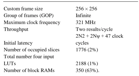
B. Implementation Results
The architecture has been mapped into Xilinx pro-grammable device (FPGA) XC4VFX140 with speed grade of 12 through the Xilinx ISE 7.1i tool. A uniform word length of 17 bits has been maintained throughout the processor to afford sufficient data depth. After pipelining the multipliers, the critical path for the processor consists of single adder, making it quite fast. A fast counter based controller was designed which handles all the address generation and other switching operations at the high speed of main data-path. Such controllers are programmable and can synchronize the control signal generation according to different video frame sizes. So other than standard N × N, they can handle standard quarter common intermediate format or common intermediate format or various different aspect ratios.
The adders from the library and device dual port block RAMs have been utilized as the principal resources for the designed processor. Simulation is performed by ModelSim XE III 6.0a, which yields a set of end results completely matching the results from MATLAB 7.0.0, where a model of the hardware is created.
The overall design report can be formulated as
Custom frame size 256 × 256
Group of frames (GOP) Infinite
Maximum clock frequency 321 MHz
Throughput Two results/cycle
Initial latency
2N2 + 2Nψ + 47 clock
cycles
Number of occupied slices 1776 (2%)
Total number four input
LUTs 2188 (1%)
Number of block RAMs 350 (63%).
C. Performance Evaluation
Among the few dedicated architectures for 3-D-DWT re-ported in literature until date, the inherent problems associated with the designs following block based approaches or having finite GOPs [9] are already discussed. Amidst the running transform methods was quite successful being convolution based, whereas [12] though promisingly formulated upon lifting, limit their discussions in the temporal processing methodology alone. Only the present design is one of the first lifting based complete 3-D-DWT architectures which enjoy no restriction on GOP.
A comparison of the present design with those available in literatures is furnished in Table I. It is worth mentioning that though [9], [10], having finite GOPs, do not represent ideal temporal transform.
From the table, the memory requirement of the presented design is found to be less than those of [9], [19] and compared to [10], requirement is less for frame sizes down to the order of 800 pixels. Even so, architecture in [10] necessitates 4N2 off-chip memories with higher read-write latency. However, it implements a lower length D-4 filter bank.
TABLE I
Comparison of the Designed Processor with Existing Works
M. Weeks Q. Dai et al. C. Parisot et al. B. Das et al. [14] J. Xu et al. Z. Taghavi Proposed
et al.∗1[9] [10] [19] [12] et al. [17]
Memory 2N2 4N2 + 9N2 0.5N2 + 6N 5N2 5N2 fast & few 5N2
requirement (P + 1) + 6l 896N + (only temporal) (spatial + (only temporal) Slow (temporal)
(spatial + 968∗2 temporal) (only temporal) + 5N
temporal) (spatial + (spatial)
Memory – – – – 5ip/T, 5ip/T, 5 ip/(2T),
Referencing 5op/T 5op/T 6 op/(2T)
at fixed FPS
(i, o/T)∗3
Throughput – – – – 1res/cycle 1res/cycle 2 res/cycle
1 Level computa- N2(P +0.5)+ – – – 4N2cycles 4N2cycles (2N2) cycles
tional latency 0.5l
1 level computing 3 N2P + – – – (P + 4)N2 (P + 4)N2 2N2 + P N2
4 2
time for P frames N2 + 3l
2 2
Operating 200 MHz – – 100 MHz – – 321 MHz
Frequency (ASIC) (0.25 µm
(Xilinx FPGA –
BiCMOS) xc4vfx140)
Adders 6l MACs 24 × 9 – – – – 26 × 3
Multipliers – 24 × 8 – Nil – – Nil
Area – – – – – – 1825 slices
Hardware – – – 100% – – 100%
Utilization
Filter bank l-length For – D-4 D-9/7 For D-9/7 D-9/7
D-9/7
GOP (P) P = 32 (max) 32 (max) Infinite Infinite Infinite Infinite Infinite
Design type Complete Complete Temporal Complete Temporal Temporal Complete
3-D 3-D processor 3-D processor processor 3-D
∗1 The 3D-DWT-I architecture.
∗2 4N2 corresponds to off-chip memory.
∗3 T symbolizes time period of computation in a standard frame rate.
TABLE II
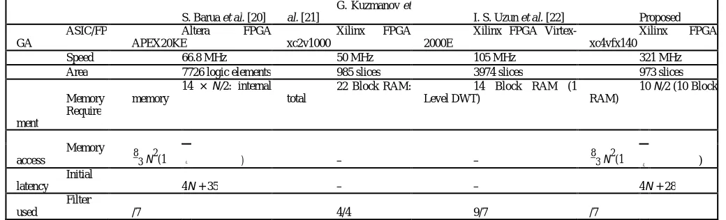
Comparison of the Spatial Sub module with Three 2-D DWT Architectures
S. Barua et al. [20]
G. Kuzmanov et
al. [21] I. S. Uzun et al. [22] Proposed
ASIC/FP GA
Altera FPGA APEX20KE
Xilinx FPGA xc2v1000
Xilinx FPGA Virtex-2000E
Xilinx FPGA xc4vfx140
Speed 66.8 MHz 50 MHz 105 MHz 321 MHz
Area 7726 logic elements 985 slices 3974 slices 973 slices
Memory
14 × N/2: internal memory
22 Block RAM: total
14 Block RAM (1 Level DWT)
10 N/2 (10 Block RAM)
Require ment
Memory
access 83 N2(1 − L ) – – 83 N2(1 − L )
Initial
latency 4N + 35 – – 4N + 28
Filter
used /7 4/4 9/7 /7
The designs referred in [12] have the same temporal buffer requirement as the proposed one. Nevertheless, in both the cases, dynamic updating of buffers data is done with the arrival of each frame whereas, as mentioned in Sections III-C and III-E, the proposed methodology succeeds in doing the transform by doing the computations once after the arrival of every two frames only. The subsequent
improvements are a halved latency and
computational time during processing and a doubled
throughput.
computing time is close to 75% of that required by [9] for large GOPs too.
Largely due to the fact that the critical path delay corresponds to a single adder, the maximum operating speed of the architecture reaches 321 MHz which makes it fastest among all. At standard rates of 30 FPS with a frame size of 256 × 256, any DWT processor with a throughput of 2 requires a minimum 1.09 MHz for real-time 1 level processing. Thus, at 321 MHz, the current design offers quite large computing potentials.
As the spatial processor module is basically a 2-D-DWT engine, comparison of this part is carried out with three other standard 2-D-DWT architectures available in the literatures andpresented in Table II. It shows that the present design has the lowest memory requirement among all and latency is lower than that of. Moreover, the proposed architecture is much faster than the rest. Comparing all the performance parameters, this architecture surely gets a cutting edge performance.
CONCLUSION
Basically the medical images need more accuracy without loosing of information. The Discrete Wavelet Transform (DWT) was based on time-scale representation, which provides efficient multi-resolution. The lifting based scheme (5, 3) (The high pass filter has five taps and the low pass filter has three taps) filter give lossless mode of information. A more efficient approach to lossless whose coefficients are exactly represented by finite precision numbers allows for truly lossless encoding. This work ensures that the image pixel values given to the DWT process which gives the high pass and low pass coefficients of the input image. The simulation results of DWT were verified with the appropriate test cases. Once the functional verification is done, discrete wavelet transform is synthesized by using Xilinx tool in Spartan 3E FPGA family. Hence it has been analyzed that the discrete wavelet transform (DWT) operates at a maximum clock frequency of 99.197 MHz respectively.
FUTURE SCOPE OF THE WORK
This work can be extended in order to increase the accuracy by increasing the level of transformations.
This can be used as a part of the block in the full fledged application, i.e., by using these DWT, the applications can be developed such as compression, watermarking, etc.
REFERENCES
[1] ISO/IEC JTC 1/SC 29/WG 1 N1646R, JPEG2000 part 1 final committee draft version 1.0, 2000. [2] C,-T.Huang, P-C, Tseng, and L,-G Chen,
“Generic RAM-based architectures for
two-dimensional discrete wavelet transform with line based method,” IEEE Trans. on Circuits and Systems, vol. 1, pp. 363- 366, 2002.
[3] Tan K C B and Arslan T., “Low power embedded extension algorithm for lifting-based discrete wavelet transform in JPEG2000,” IEEE Electronic Letters, Vol...37, pp.1328-1330, 2002.
[4] Xuguang Lan, Nanning Zheng and Yuehu Liu, “Low-power and high-speed VLSI architecture for lifting-based forward and inverse wavelet transform,” IEEE Trans. on Consumer Electronics, Vol.51, pp.379-385, 2005
[5] Chin-Fa Hsieh, Tsung-Han Tsai and Chih-Huang Lai, “ Implementation of an efficient DWT using a FPGA on a Real-time Platform,” IEEE, ICICIC, Second International Conference on, pp. 235-235, 2007
[6] P.Y Chen, “VLSI implementation for
one-dimensional multilevel lifting based wavelet
transform, “IEEE Trans. on Computers, vol. 53, pp.386- 398, 2004.
[7] Peng Cao, Xin Guo, and Chao Wang, “Efficient architecture for two-dimensional discrete wavelet transform based on lifting scheme,” IEEE 7th International Conference on, pp. 225-228, Oct. 2007.
[8] B.-F. Wu and C.F. Lin, “A high-performance and memory-efficient pipeline architecture for the 5/3 and 9/7 discrete wavelet transform of JPEG2000 codec,” IEEE Trans. on Circuit and Systems for Video Technology, vol. 15, pp. 1615-1628, Dec. 2005.
[9] Benderli O, Tekmen Y C and Ismailoglu N. “A real time, low latency, FPGA implementation of the 2D discrete wavelet transformation for streaming image applications,” IEEE workshop on Signal processing systems, pp. 384-389, Sept. 2003.