I
---
- - -
-
-
-
-
- - -
- --
---
---_
.
-GA34-0289-1 File No. S1-16
IBM Series/1
4956 Processor Models E and E 1 0
Description
-~---
- - -
-
-
- -
-
-
- - -
-
---
---
--_.-GA34-0289-1
File No. S1-16
IBM Series/1
4956 Processor Models E and E
10
Description
Second Edition (January 1986)
Use this publication for the purpose stated in the preface.
Preface
Prerequisite Publication
This publication describes the unique functional characteristics and the optional features of the IBM Series/l 4956 Processor Models E and EtO. This publication also provides reference information about the possible configurations and feature operations of the processor. Refer to the IBM Series/l Principles of Operation,
GA34-0 152, for the common Series/l processor functional characteristics and instructions.
This publication is intended primarily as a reference manual for experienced programmers who require machine code information to plan, correct, and modify programs written in the assembler language. The reader should understand data processing terminology and be familiar with binary and hexadecimal numbering systems.
Chapter 1, "Introduction," contains a general description of the processor, processor storage, and processor features. This chapter also contains information about changes to the programming instruction set.
Chapter 2, "Processor Storage Addressing Using the Relocation Translator," describes the relocation translator, including:
Relocation addressing
Storage-protection mechanism
Error-recovery considerations.
Chapter 3, "Console," describes the keys, switches, and indicators for the basic console and the optional programmer console. Typical manual operations, such as storing into and displaying processor storage, are presented.
Chapter 4, "Diagnose (DIAG) Instruction," describes the Diagnose instruction.
Appendix A, "Instruction Execution Times," contains information for determining instruction execution times and instruction throughput.
Appendix B, "Software Notes," lists some software notes for the processor.
Appendix C, "Error Log," describes the error log and explains its use as an aid in isolating errors.
Contents
Chapter 1. Introduction 1 - 1 Processor Description 1-4 Storage Cards 1-7
Card Plugging Assignments I-X
Input/Output Units, I/O Features, and Processor Options 1-9 Program-Controlled Mode Switching 1-10
Address Key Register (AKR) 1-10 Processor Status Word (PSW) Register I-II Modified Instructions 1-12
Set Address Key Register (SEAKR) 1-12 Copy Address Key Register (CPAKR) 1-16 Set Segmentation Register (SESR) 1-20 Copy Segmentation Register (CPSR) 1-23 Copy Processor Status and Reset (CPPSR) 1-26 Enable (EN) 1-27
Disable (DIS) 1-2X New Instructions 1-29
ARlB Instruction Format 1-29 ARlBON Instruction Format 1-31 ARlBOFF Instruction Format 1-31 ARlB Execution 1-32
Chapter 2. Main Storage Addressing Using the Relocation Translator 2-1
Translator Description 2-1 Storage Mapping 2-2 Relocation Addressing 2-2
I/O Storage Access Using the Relocation Translator 2-4 Status of Translator After Power Transitions and Resets 2-4 Error-Recovery Considerations 2-5
Invalid Storage Address ((SA) 2-5 Protect Cheek 2-5
Address Space Management 2-6 Active Address Key 2-6
Equate Operand Spaces (EOS) 2-6 Address Space 2-7
Address Key Values After Interrupts 2-9
Chapter 3. Console 3- 1 Basic Console 3-2
Indicators 3-3 Programmer Console 3-3
Console Display 3-4 Indicators 3-5
Combination Keys/Indicators 3-6 Keys and Switehes 3-12
Displaying Registers 3-17 Storing Into Registers 3-17
Displaying Segmentation Registers 3-1 X Storing Into a Segmentation Register 3-20 Displaying Main Storage Locations 3-22 Storing Into Main Storage 3-24
Chapter 4. Diagnose (DIAG) Instruction 4-1 Storage Select 4-3
Storage Select Word 4-3
Storage Select Byte/ECC Code Bits 4-4 Local Storage Register Select 4-5
Channel Select 4-6 Set System I D 4-6 Error Log Select 4-7 Indicators 4-7
Program-Check Condition 4-7
Appendix B. Software Notes B-1
Appendix C. Error Log C-l Purpose C-I
Structure C-I
Machine Check C-2 Program Check C-2
Stall Detector/Timer Overrun Error C-2 Format of Log Entries C-3
Machine Check C-3 Program Check C-3 Priority Interrupt Entries C-4 Operate I/O Entries C-4
Chapter 1. Introduction
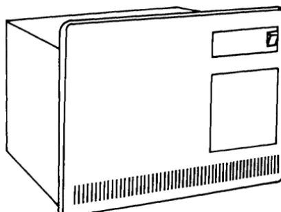
The IBM Series/l 4956 Processor Models E and E 1 0 are compact general-purpose computers. The models are the same, except for basic storage. Model E has 256 or 512 kilobytes of basic storage; Model EI0 has 1024 kilobytes of basic storage. The processor is microcode-controlled for both automatic functions and program
instruction functions. It occupies the full width of a standard 483-millimeter
(19-inch) rack (see Figure 1-1). It contains thirteen card sockets for data channel
features and a channel repower card. Three of the thirteen card sockets can also be used for additional processor storage cards.
[
~
o
1111111" II"" /II I
/II" """"" """" """ "'""
[image:8.621.207.412.222.376.2]The processor has the following characteristics:
• Four priority interrupt levels, with independent registers and status indicators for each level.
• Automatic and program-controlled level switching.
• An instruction set that includes stacking and linking facilities, multiply and divide, variable-field-length byte operations, and a variety of arithmetic and branching instructions.
Supervisor and problem states.
A basic console that is a standard feature; a programmer console that is an optional feature.
Basic main storage and up to three additional storage increments of either 256 kilobytes, 512 kilobytes, or 1024 kilobytes, with a maximum possible storage of 2048 kilobytes (2 megabytes).
A storage address relocation translator that allows addressing of main storage larger than 64 kilobytes.
Program-controlled mode switching that allows the user to specify the maximum mappable storage range:
512K bytes in 3-bit mode
1024K bytes (1 MB) in 4-bit mode
• Prefetching instruction stream. (Refer to Appendix B.)
An error correction code (ECC) that is implemented on the storage card to provide the capability for single-bit error correction and double-bit error detection.
• An error log that provides a history of errors that have occurred since power-on. (Refer to Appendix C.)
A clock/comparator with four instructions provided to set or copy the clock and comparator.
• Channel capability as follows:
Note: The burst output and burst input data rates are reduced from the values shown by data channel attachment characteristics, channel loading during instruction processing, channel repowering, and processor storage refresh requirements.
Throughput that is approximately 50% greater than previous models of the 4956.
A redefined 16-bit address key register (AKR).
A redefined 16-bit processor status word (PSW) register.
Several instructions modified for 4-bit mode:
Set Address Key Register (SEAKR) Copy Address Key Register (CP AKR) Set Segmentation Registers (SESR) Copy Segmentation Registers (CPSR) Enable (EN)
Disable (DIS)
Copy Processor Status and Reset (CPPSR)
Note: For an explanation of the standard Series/l instruction set, refer to
IBM Series/l Principles of Operation, GA34-0152. Three new instructions in the instruction set:
Address Resolution with Indirect Branch (ARIB)
Processor Description
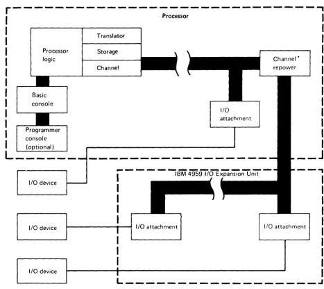
The basic processor includes the processor card, a basic storage card, and a basic console. Figure 1-2 shows a block diagram of the processor and an IBM Series/l 4959 Input/Output Expansion Unit.
r---,
ProcessorProcessor logic
Basic console
Programmer console
( tional)
L _____ _
I/O device
I/O device
I/O device
Translator Storage
Channel
1/0
attachment
---
IBM 4959 I/O Expansion UnitChannel *
I/O attachment 1/0 attachment
I
I
I
I
I
I
I
I
I
I
L _ _ _ _ _ _ _ _ _ _ _ _ _ _ _ _ _ _
~* Required with an expansion unit.
[image:11.627.80.548.133.549.2]Four priority interrupt levels (0-3) are implemented in the processor. Each level has an independent set of machine registers. Level switching can occur in two ways: (1) by program control, or (2) automatically upon acceptance of an I/O interrupt request. The interrupt mechanism provides 256 unique entry points for I/O devices.
Note: A Prepare command to levels 4-15 is executed so that condition
code reporting occurs; however, the Prepare command is not executed at the addressed device and effectively results in a no-operation.
The processor instruction set contains a variety of instruction types. These include: bit manipulation
shift branch
register immediate storage immediate register to register register to storage storage to register storage to storage system register to storage mUltiple register to storage variable byte field.
Supervisor and problem states are implemented, with appropriate privileged instructions for the supervisor.
The basic console is intended for dedicated systems that are used in a primarily unattended environment. Only minimal controls are provided. A programmer console, which can be added as a feature, provides a variety of indicators and controls for operator-oriented systems.
An error correction code (ECC) is implemented on the storage card. ECC gives the storage card the capability of single-bit error correction and double-bit error detection. ECC provides the user a higher system availability.
Note: When a double-bit error in storage is detected during a processor read, a machine check interrupt occurs with PSW bit 8 set to 1 (storage parity error).
There is no storage-protect feature in the processor. However, there is a read-only protect capability provided by the address translator when it is enabled.
Note: Execution of the Set Storage Key (SESK) and Copy Storage Key (CPSK) instructions results in a no-operation.
I/O devices are attached to the processor through the processor data channel. The data channel directs the flow of information between the I/O devices, the
The data channel supports:
Direct program control operations. Each Operate I/O instruction transfers a byte or word of data between main storage and the device. The operation may or may not terminate in an interrupt.
• Cycle-steal operations. Each Operate I/O instruction initiates multiple data
transfers between main storage and the device. The maximum cycle-steal transfer per device control block (DCB) is 65,535 bytes. Cycle-steal operations are overlapped with processor operations and always terminate in an interrupt.
• Interrupt servicing. Interrupt requests from the devices, along with cycle-steal
Storage Cards
The processor supports three different size storage cards: 256 KB, 512 KB, and 1024 KB. The processor has a maximum of 2048 KB of storage. Any combination of storage cards may be used (with the exception of one 512 KB card with three 256 KB cards) to obtain the desired system storage size, up to the maximum of 2048 KB. (The relocation translator must be enabled to select addresses above 64K bytes.)
Several other rules apply for proper storage card plugging:
All storage cards are plugged in decrementing order from the processor card.
• No card sockets may be left unused between storage cards.
• Storage cards must be plugged in the order for which they are jumpered.
Card Plugging Assignments
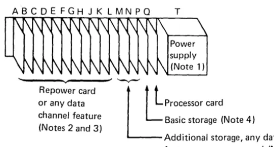
The processor unit contains power and space for additional features. The IBM Series/1 4959 Input/Output Expansion Unit and the IBM Series/1 4965 Storage and I/O Expansion Unit are available for adding additional features, if desired. Figure 1-3 shows the card plugging assignments for the processor.
A~CDEFGHJKLMNPO T
~---~---' ~ Repower card
or any data channel feature
(Notes 2 and 3)
~
l
Processor cardL
Basic storage (Note 4)Additional storage, any data channel feature, or repower card (Notes 5-8)
Figure 1-3. Card Plugging Assignments
Notes:
1. The pluggable high-frequency power supply plugs into card socket T.
2. If a channel repower card is used, it must be plugged to the left of and adjacent
to the leftmost I/O card installed.
3. A maximum of five serially-connected channel repower features can be driven by each processor. Any processor system that includes an IBM I/O expansion unit with the two-channel switch feature is limited to three channel repower features.
4. The processor contains 256 KB (kilobytes), 512 KB, or 1024 KB of basic storage in socket P.
[image:15.624.185.456.146.291.2]Input/ Output Units, I/O Features, and Processor Options
A variety of I/O units and features, plus several processor options, are available for use with the processor. For a list and description of system units and features, refer to the IBM Series/l System Selection Guide, GA34-0143, and the IBM
Series/l Digest, G360-0061. Detailed information about I/O units and features can be found in separate publications. The order numbers for these publications are contained in the IBM Series/l Graphic Bibliography, GA34-0055.
The floating-point feature is one of the available options. If the floating-point
feature is installed, refer to Appendix A for instruction execution times. For a detailed description of this feature, refer to the IBM Series/l Principles of
Program-Controlled Mode Switching
Address Key Register (AKR)
Program-controlled mode switching allows the user to specify the maximum mappable storage range:
In 3-bit mode, the maximum mappable storage is 512K bytes. Operand 1 key (OPIK), operand 2 key (OP2K), and instruction space key (lSK) are specified in three bits. The translator uses 3 bits from the active address key and the five high-order bits of the logical address to select one of 256 segmentation registers when the translator is enabled.
In 4-bit mode the maximum mappable storage is 1024K bytes (1 MB). In 4-bit
mode, OPIK, OP2K, and ISK are specified in four bits. Eight additional stacks of 32 registers per stack are available for I/O operations. This allows 512K bytes of storage to be mapped for I/O only, independent of program mapping. Bit 7 of the processor status word (PSW) indicates which mode the processor is currently in:
When bit 7 is a 0, the processor is in 3-bit mode. When bit 7 is aI, the processor is in 4-bit mode.
When both bit 7 and bit 14 (translator bit) are 1 's, the I/O translator is enabled.
The address key register (AKR) contains 16 bits. It is formatted as follows:
For 3-bit mode: For 4-bit mode:
Bit Data Bit Data
0 Equate operand spaces 0 Equate operand spaces
1 0 1 0
2 0 2 0
3 0 3 0
4 0 4 OPIK bit 0
5 OPIK bit 0 5 OPIK bit 1
6 OPIK bit 1 6 OPIK bit 2
7 OPIK bit 2 7 OPIK bit 3
8 0 8 OP2K bit 0
9 OP2K bit 0 9 OP2K bit 1
10 OP2K bit 1 10 OP2K bit 2
11 OP2K bit 2 11 OP2K bit 3
Processor Status Word (PSW) Register
The processor status word (PSW) register contains 16 bits. It is formatted as
follows:
Bit Data
0 Specification check
1 Invalid storage address
2 Privilege violation
3 Protect check
4 Invalid function
5 Floating point exception
6 Stack exception
7 4-bit mode enabled
8 Storage parity check
9 0
10 Processor control check
11 I/O check
12 Sequence indicator
13 Auto IPL
14 Translator enabled
Modified Instructions
Modifications have been incorporated into several Series/l instructions pertaining to their use with the processor. These modifications apply only for 4-bit mode operation; they do not apply for 3-bit mode operation. The instructions that have been modified are:
Set Address Key Register (SEAKR) Copy Address Key Register (CP AKR) Set Segmentation Registers (SESR) Copy Segmentation Registers (CPSR) Enable (EN)
• Disable (DIS)
Copy Processor Status and Reset (CPPSR).
Note: For an explanation of the standard Series/l instruction set, refer to
IBM Series/l Principles of Operation GA34-0152.
Set Address Key Register (SEAKR)
System Register/Register Format
The Set Address Key Register (SEAKR) instruction has two formats:
System register/register format for operations that load data from a specified register into the AKR.
System register/storage format for operations that load data from main storage into the AKR.
The system register/register format is:
Mnemonic Syntax Instruction name K-field
SEAKR reg Set Address Key 011
Register
Extended
mnemonic Syntax Instruction name K-field
SEISK reg Set Instruction 000
Space Key
SEOOK reg Set Operand 1 Key 010
For 3-bit mode:
K-field Address key register field name Bits
000 Instruction space key 13-15
001 Operand 2 key 9-11
010 Operand 1 key 5-7
011 Address key register 0-15
100 Should not be used
101 Should not be used
110 Should not be used
111 Should not be used
For 4-bit mode:
K-field Address key register field name Bits
000 Instruction space key 12-15
001 Operand 2 key 8-11
010 Operand 1 key 4-7
011 Address key register 0-15
100 Should not be used
101 Should not be used
110 Should not be used
111 Should not be used
If the K-field specifies a specific field within the AKR, bits 13-15, for 3-bit mode,
or bits 12-15, for 4-bit mode, from the register specified by the R-field are loaded
into the AKR field. If the K-field specifies the entire AKR, bits 0-15 from the
specified register are loaded into the AKR. Indicators: The indicators are not changed.
Program Checks: This instruction format has the following program check:
Privilege violate - The instruction is encountered while in problem state. The
System Register/Storage Format
Mnemonic Syntax Instruction name
SEAKR addr4 Set Address Key Register
Extended
mnemonic Syntax Instruction name
SEISK addr4 Set Instruction Space Key
SEOOK addr4 Set Operand 1 Key SEOTK addr4 Set Operand 2 Key
IOPcode
o
1 0 111K
IRB lAM
I~u~ct~ono
I
0 4 5 7 8 9 101112 15
A ddresslD isplacement
Displacement 1 Displacement 2
16 2324 31
K-field 011 K-field 000 010 001
The address key register (AKR) field specified by the K-field is loaded from the word location in main storage that is specified by the effective address. The contents of the word in main storage are not changed.
Note: The K-field can specify either a field within the AKR or an entire AKR.
For 3-bit mode:
K-field 000 001 010 011 100 101 110
Address key register field name Instruction space key
Operand 2 key Operand 1 key Address key register Should not be used Should not be used Should not be used
111 Should not be used
Bits
For 4-bit mode:
K-field 000 001 010
all
100 101 110 111
Address key register field name Instruction space key
Operand 2 key Operand 1 key Address key register Should not be used Should not be used Should not be used Should not be used
Bits 12-15 8-11
4-7
0-15
If the K-field specifies a specific field within the AKR, bits 13-15, for 3-bit mode,
or bits 12-15, for 4-bit mode, from the word location in main storage are loaded
into the AKR field. If the K-field specifies the entire AKR, bits 0-15 from the
word location in main storage are loaded into the AKR. Indicators: The indicators are not changed.
Program Checks: This instruction format has the following program checks:
Invalid storage address - One or more words of the instruction or the effective
address are outside the installed storage size of the system. The instruction ends and a program check interrupt occurs with invalid storage address set in the PSW.
Privilege violate - The instruction is encountered while in problem state. The
instruction is suppressed and a program check interrupt occurs with privilege violate set in the PSW.
Specification check - The effective address or indirect address results in an
Copy Address Key Register (CPAKR)
System Register/Register Format
The Copy Address Key Register (CPAKR) instruction has two formats: System register/register format for operations that load data from the AKR
into a specified register.
System register/storage format for operations that load data from the AKR into main storage.
The system register/register format is:
Mnemonic Syntax Instruction name K-field
CPAKR reg Copy Address Key all
Register
Extended
mnemonic Syntax Instruction name K-field
CPISK reg Copy Instruction 000
Space Key
CPOOK reg Copy Operand 1 Key 010
CPOTK reg Copy Operand 2 Key 001
lop
code011 1
11K
IR
I
Function
1 1 0 1
01
0 4 5 7 8 1011 15
The contents of the address key register (AKR) field specified by the K-field are loaded into the register specified by the R-field. The contents of the AKR are not changed.
Note: The K-field can specify a field within the AKR or the entire AKR.
For 3-bit mode:
K-field
000 001 010
all
Address key register field name Instruction space key
Operand 2 key Operand 1 key Address key register
Bits
For 4-bit mode: K-field
000 001 010 011 100
Address key register field name Instruction space key
Operand 2 key Operand 1 key Address key register Should not be used
101 Should not be used
110 Should not be used
111 Should not be used
Bits 12-15 8-11
4-7
0-15
If the K-field specifies a specific field within the AKR, the specified field is loaded
into bits 13-15, for 3-bit mode, or bits 12-15, for 4-bit mode, of the register specified in the R-field. Bits 0-12, for 3-bit mode, or bits 0-11, for 4-bit mode,
are set to O's. If the K-field specifies the entire AKR, the AKR is loaded into the
register.
Indicators: The indicators are not changed.
Program Checks: This instruction format has the following program check:
Privilege violate - The instruction is encountered while in problem state. The
System Register/Storage Format
The system register/storage format is:
Mnemonic Syntax Instruction name
CP AKR addr4 Copy Address Key Register
Extended
mnemonic Syntax Instruction name
CPISK addr4 Copy Instruction Space Key
CPOOK addr4 Copy Operand 1 Key CPOTK addr4 Copy Operand 2 Key
lop
codeo
1 0 111K
I
RBI
AMI~u~ct~on
0I
0 4 5 7 8 9 101112 15
A ddresslD isplacement
Displacement 1 Displacement 2
16 2324 31
K-field 011 K-field 000 010 001
The contents of the address key register (AKR) field specified by the K-field are stored in the word location specified by the effective address. The contents of the AKR are not changed.
Note: The K-field can specify a field within the AKR or the entire AKR.
For 3-bit mode:
K-field 000 001 010 011 100 101 110
Address key register field name Instruction space key
Operand 2 key Operand 1 key Address key register Should not be used Should not be used Should not be used
111 Should not be used
Bits
13-15
9-11
For 4-bit mode:
K-field Address key register field name Instruction space key
Operand 2 key
Bits 000
001 010 011 100
Operand 1 key Address key register Should not be used
12-15 8-11
4-7
0-15
101 Should not be used 110 Should not be used 111 Should not be used
If the K-field specifies a specific field within the AKR, the specified field is stored in bits 13-15, for 3-bit mode, or bits 12-15, for 4-bit mode, of the word location in main storage. Bits 0-12, for 3-bit mode, or bits 0-11, for 4-bit mode, of the word in main storage are set to O's. If the K-field specifies the entire AKR, the AKR is stored in the word location in main storage.
Indicators: The indicators are not changed.
Program Checks: This instruction format has the following program checks:
Invalid storage address - One or more words of the instruction or the effective address are outside the installed storage size of the system. The instruction ends and a program check interrupt occurs with invalid storage address set in the PSW.
Privilege violate - The instruction is encountered while in problem state. The instruction is suppressed and a program check interrupt occurs with privilege violate set in the PSW.
Set Segmentation Register (SESR)
The syntax for this instruction is:
SESR reg,addr4
0 4 5 7 8 9 10 11 12 15
A ddress/D isplacement
Displacement 1 Displacement 2
16 2324 31
This instruction loads the contents of one or more doubleword storage locations, the first of which is specified by the effective address, into the segmentation registers specified by the contents of the register specified by the R-field.
For processors with 3-bit keys enabled, the format of the register specified by the R-field is:
o
4 5 7 8 9 10 1415I
~~::I
I
Key
I
0 0I
CountI
0I
Key bits 0 1 2
Bits 0-7 form the number of the segmentation register to be loaded (0-255). This number is comprised of 3-bits from the address key (values 0-7) and the five high-order bits of the logical storage address which is the logical segment (values 0-31). Bits 8, 9, and 15 of the register are reserved and must be set to O's. Bits 10-14 specify the number of contiguous segmentation registers to be set from contiguous doubleword storage locations.
Notes:
1. The count is equal to count plus 1. For example a count of 0 loads one register.
2. If AM=O 1, the register selected by the RB field is incremented by 4 for each
For 4-bit mode, the format of the register specified by the R-field is:
o
Logical sector
4 5
Key bits 1 23 0
8 9 10 1415
Key Count
Note: Bit 8 is the most significant bit in the key field, and bit 7 is the least significant bit. For example, 0011 in the key field would indicate stack 9. Bits 0-8 form the number of the segmentation registers to be referenced (0-510 where the value of key bit 0 provides a select control between the first and second 256 segment register groups. This number is comprised of four bits from the address key (values 0-15) and the five high-order bits of the logical storage address, which is the logical segment (values 0-31). Bit 9 of the register is reserved and must be set to O.
Bits 10-14 specify the number of contiguous segmentation registers to be set from
contiguous doubleword locations (count plus O. The instruction ends when the
count is exhausted or when register 31 is loaded.
Bit 15, when aI, indicates that the segmentation register stack referenced is the
one reserved for I/O. Bit 8 (in the key field) is ignored in this case.
Notes:
1. If AM=OI, the register selected by the RB field is incremented by 4 for each
segmentation register set. 2. All indicators are unchanged.
The first word (bits 0-15) of the specified double word that is loaded into the selected segmentation register has the following format:
I
Phvsical segment addresso
1
=
valid----=1
r
T
1 = r e a d - o n l 2 J
(must be 0)
\0 0 0 0 0 0 0 0 0 0 0 0 0 0 0 0\
16 31
The segment address (bits 0-12) contains the high-order bits of the physical address.
Bit 13, if aI, signifies that the contents of the segmentation register are valid, and
translation can be performed. If an attempt is made to use a segmentation register
with bit 13 set to 0, a program check interrupt occurs with invalid storage address set in the PSW.
Bit 14, if aI, signifies that the block is read-only. If an attempt is made to write
in problem state, a program check interrupt occurs, with protect check set in the PSW. When in supervisor state or on a cycle-steal access, bit 14 is ignored. The contents of main storage can be changed.
The second word (bits 16-31) of the specified doubleword should be set to D's.
Indicators: The indicators are not changed.
Program Checks: This instruction has the following program checks:
Invalid function - In the supervisor state, an attempt has been made to invoke
this instruction when the translator is not enabled.
Invalid storage address - One or more words of the instruction or the effective
address are outside the installed storage size of the system. The instruction ends and a program check interrupt occurs with invalid storage address set in the PSW.
Privilege violate - The instruction is encountered while in problem state. The
instruction is suppressed and a program check interrupt occurs with privilege violate set in the PSW.
Specification Check - The effective address or indirect address results in an
Copy Segmentation Register (CPSR)
The syntax for the register/storage format is:
CPSR reg,addr4
0 4 5 7 8 9 1011 12 15
A ddress/D isplacement
Displacement 1 Displacement 2
16 2324 31
This instruction stores the contents of one or more segmentation registers, specified by the contents of the register specified by the R-field, into contiguous double word storage locations, the first of which is specified by the effective address.
In the 3-bit mode, the format of the general register specified by the R-field is:
o
Logical sector
4 5 7 8 9 10
1 Key 10 0 1
1415
Count Key bits 0 12
Bits 0-7 form the number of the segmentation register to be copied (0-255). This number is comprised of 3-bits from the address key (values 0-7) and the five high-order bits of the logical storage address which is the logical segment (values 0-31). Bits 8, 9 and 15 of the register are reserved and must be set to O.
Bits 10-14 specify the number of contiguous segmentation registers to be copied to contiguous doubleword storage locations and is equal to the count plus 1 (for example a count of zero loads one doubleword storage location). The instruction ends when the count is exhausted or when register 31 of the key space has been copied.
Note: If AM=Ol, the register selected by the RB field is incremented by 4
for each segmentation register copied.
For processors with 4-bit mode enabled, the format of the register specified by the R-field is:
o
Logical sector
4 5
Key
8 9 10 1415
Count Key bits 1 23 0
is the logical segment (values 0-31). Bit 9 of the register is reserved and must be set to O.
Bit 15, when set to 1, indicates that the segmentation register stack referenced is
the one reserved for I/O. Bit 8 (in the key field) is ignored in this case.
Bits 10-14 specify the number of contiguous segmentation registers to be copied to contiguous doubleword storage locations, with the count equal to the count plus
1 (for example if the count is zero, one doubleword storage location is loaded).
Note: If AM=OI, the register selected by the RB field is incremented by 4
for each segmentation register copied.
The first word of the specified doubleword that is copied from the selected segmentation register has the following format:
I
Segment addresso
1 = valid
2J12
r
14 15
1 =
read.onIY~
(must be 0)
1000 0 0 0 0 0 0 0 0 0 0 0 0 0
I
16 31
The segment address (bits 0-12) contains the high-order bits of the physical address, which is used by the translator to select a 2K-byte block of main storage. Bit 13, if a 1, signifies that the contents of the segmentation register is valid, and
the translation can be performed. If an attempt is made to use a segmentation
register in which bit 13 is a 0, a program check interrupt occurs,with invalid storage address set in the PSW.
Bit 14, if aI, signifies that the block is read-only. If an attempt is made to write
into the block when bit 14 of the associated segmentation register is a 1 and while in problem state, a program check interrupt occurs, with protect check set in the PSW. When in supervisor state or on a cycle-steal access, bit 14 is ignored; the contents of main storage can be changed.
Indicators: The indicators are not changed.
Program Checks: This instruction has the following program checks:
Invalid function - In the supervisor state, an attempt has been made to invoke
this instruction when the translator is not enabled.
Invalid storage address - One or more words of the instruction or the effective
address are outside the installed storage size of the system. The instruction ends and a program check interrupt occurs with invalid storage address set in the PSW.
Privilege violate - The instruction is encountered while in problem state. The
instruction is suppressed and a program check interrupt occurs with privilege violate set in the PSW.
Specification check - The effective address or indirect address results in an
Copy Processor Status and Reset (CPPSR)
The syntax for this instruction is:
CPPSR addr4
Op code
o
1 0 1o
4 5 7 8 9 101112 15A ddress/D isplacement
Displacement 1 Displacement 2
16 2324 31
The contents of the processor status word (PSW) are stored at the word location in main storage specified by the effective address.
This instruction resets PSW bits 0-6 and 8-12. of Bits 7 and 13-15 are not changed. Bits 5 - 7 of the instruction are not used and should be set to O's. Indicators: The indicators are not changed.
Program Checks: This instruction has the following program checks:
Invalid storage address - One or more words of the instruction or the effective
address are outside the installed storage size of the system. The instruction ends and a program check interrupt occurs with invalid storage address set in the PSW.
Privilege violate - The instruction is encountered while in problem state. The
instruction is suppressed and a program check interrupt occurs with privilege violate set in the PSW.
Specification check - The effective address or indirect address results in an
Enable
(EN)The syntax for this instruction is:
EN ubyte
o
4 5 7 8 15The parameter field bits have the following significance:
Bit Significance
8 Not used
9 Not used
10 Enable 4-bit mode (PSW bit 7= 1)
11 Not used
12 Enable storage protect
13 Enable equate operand spaces
(AKR bit
°
set to 1)14 Enable translator (PSW bit 14 set to 1)
15 Enable summary mask (LSR bit 11 set to 1)
Note: Bits not used must be set to O's.
If bit 12 is set to 1, the relocation translator (if enabled) is disabled and bit 14 is not checked.
If bit 14 is set to 1, and bit 12 is set to 0, the relocation translator is enabled. If parameter bit 14 and parameter bit 10 are both 1 's or if parameter bit 14 and PSW bit 7 are both 1 's, the I/O translator is enabled.
If parameter bit 14 is a 1, parameter bit 10 is a 0, and PSW bit 7 is a 0, the I/O translator is not enabled.
Indicators: The indicators are not changed.
Program Checks: This instruction has the following program check:
Privilege violate - The instruction is encountered while in problem state. The
Disable (DIS)
The syntax for this instruction is:
DIS ubyte
I
~p 1co~e
0 0I
~unc
11
Parametero
4 5 7 8 15The bits in the parameter field have the following significance:
Bit Significance
8 Not used
9 Not used
10 Disable 4-bit mode (PSW bit 7 =0)
11 Not used
12 Disable storage protect
13 Disable equate operand spaces
(AKR bit 0 set to 0)
14 Disable translator (PSW bit 14 set to 0)
15 Disable summary mask (LSR bit 11 set to 0)
Note: Bits not used must be set to O's.
If a Disable instruction immediately follows an Enable summary mask instruction,
the interrupt disable function may occur prior to the time that an interrupt can be accepted. Thus, at least one other instruction (for example, no-op) must be inserted between the Enable summary mask and Disable instructions to ensure the occurrence of the interrupt.
If parameter bit 14 is set to 1 and the relocation translator is enabled (bit 14 of the
PSW is a 1), then the translator is disabled and bit 14 of the PSW is set to a O. If
parameter bit 14 is a 1, the
1/0
translator is always disabled.If PSW bit 14 is a 1 and parameter bit 10 is aI, the I/O translator is disabled.
Indicators: The indicators are not changed.
New Instructions
ARIB Instruction Format
The processor has three additional instructions:
Address Resolution with Indirect Branch (ARIB)
Address Resolution with Indirect Branch-On (ARIBON) Address Resolution with Indirect Branch-Off (ARIBOFF).
The ARIB instruction is a three-word instruction that performs the mapping actions. This instruction is intended to be used exclusively by the operating system. Mapping actions are the operation of fetching a command with an op code,
operand 1, operand 2, and resolving the addressing modes used by those operands. The format of the instruction follows:
Word 1 1
a
1 1 1 1 1a a a
11 0a
1a
1 1 1 1I
o
4 5 7 8 10 11 15Word
21
Displacement 116
Word
31
TBLADDR address32
1 Displacement 2
23 24 31
47
The instruction uses the values of displacement 1, displacement 2, and the address of the first word of the branch table TBLADDR for loading the ARIB instruction work registers, where:
Displacement 1 is the index parameter displacement byte used with the control block designated by R2.
Displacement 2 is the displacement byte parameter used with the control block designated by R2 to store Rl.
Register and Storage Conventions
The register conventions used by the mapping routine of the ARIB are as follows: Entry conditions:
R 1 is the address of first word of the current command for ARIB. R2 is the address of a control block.
Exit conditions:
R 1 and R2 are unchanged.
R3 is the resolved address of operand 1. R4 is the resolved address of operand 2.
R5 is the contents of storage word pointed to by R 1.
R6 is the TBLADDR index value that is defined as the command op code, multiplied by 2.
IAR is the contents of the storage location at the effective address TBLADDR, plus the contents of R6.
Storage location is the effective address of the contents of R2, plus
displacement 2 of ARIB instruction word 2, containing the contents of R 1. Indicators: The indicators are not changed.
Program Checks: This instruction has the following program checks:
Invalid function - The instruction encountered the ARIB mode condition off.
The instruction is suppressed, and a program check interruption occurs, with invalid function set in the PSW.
Invalid storage address - One or more words of the instruction or any of the
effective addresses is outside the installed storage size of the system. The indirect branch does not occur, and the instruction is terminated. Some of the level registers may have changed.
Specification check - The effective address or indirect address results in an
ARIBON Instruction Format
The ARIBON instruction is a two-word instruction that activates the address resolution and indirect branch feature by turning on an internal flag that allows execution of the ARIB instruction. This mode is only reset by an IPL, a system reset, a power-on reset, or the ARIBOFF instruction. The ARIBON instruction is intended to be used by the operating system, and it may be issued in either the problem state or the privilege state.
10 1 1 1 110 0 011 0 010 1 1 1 01
o
4 5 7 8 10 11 1510 0 0 0 0 0 0 0 0 0 0 0 0 0 0 1 1
16 31
Word 2 bits 0-14 are reserved and must be set to O. Bit 15 must be set to 1.
Indicators: The indicators are not changed.
ARIBOFF Instruction Format
The ARIBOFF instruction is a two-word instruction that deactivates the address resolution and indirect branch feature by turning off the ARIBON flag. This instruction is intended to be used by the operating system, and it may be issued in either the problem state or the privilege state.
10
1 1 1110
a
011
o
010 1
1 101
0 4 5 7 8 10 11 15
10
a a a a a a a a a a a a a a
01
16 31
Word 2 is set to all O's.
ARIB Execution
The required operations for the ARIB instruction are as follows:
Initialization: Prior to the invocation of the ARIB instruction, the operating system must issue the ARIBON instruction. For ordinary usage, this should be part of the IPL procedure.
Setup: The content of R1 is placed in the main storage location designated by the effective address of displacement 2 of the ARIB instruction word 2, plus the control block address in R2 and with OP2K to generate the physical storage address.
Note: There is no use of this storage address during the ARIB instruction, and the R 1 register is maintained intact.
Command: A high level command is fetched from the main storage location specified by the contents of R1, and placed into R5. The contents of R5 are defined as a command with the following definition.
o
1 3 4 5 6 7 8 15Bit
o
1-3 4-5 6-7
8-15
Meaning
Operand 2 type (1 =constant, O=address)
Not defined .
Register flag for operand 2 Register flag for operand 1 Operation code function
The I-field of the op code indicates to the mapping routine that the second operand is an immediate value. The OPR2 and OPR1 fields are used to define the
addressing mode used for each of the operands.
The op code function field is used by the mapping routine to generate the index value for displacement in the table "TBLADDR."
The 2-bit register flag for each operand is defined as follows: Field value
o
1
2
Meaning
Register not specified
Operand Address Resolution: Operand 1 is fetched from the main storage location at
the effective address specified by the contents of R 1 plus 2, and placed into R3.
Operand 2 is fetched from the main storage location specified by the contents of R 1 plus 4, and placed into R4. If operand 2 is a constant, R4 contains the value R 1 plus 4, which is a pointer to that constant.
If operand 1 is an indexed value (parameter or index register), the setup routine adds the contents of the selected register (operand 1 or operand 2) to R3. If
operand 2 is an indexed value (parameter, index register), the setup routine adds the contents of the selected register (operand 1 or operand 2) to R4.
These are accomplished as follows: An effective address is generated by adding displacement 1 with the contents of level register R2. The effective address is used with OP2K to generate the physical address. The contents of main storage at the generated address contains an address which points to the first word of a pair of index values. Reference to this storage location is required whenever command word bits 4-5 or 6-7 are respectively non-zero. Another address is then formed by adding to these contents the bits 4-5, for operand 1, or bits 6-7, for operand 2, to the low-order address word bit positions, thus adding bit positions 13, 14, and 15 where bit 15 is O. This address is then used to fetch the storage location that is added to the appropriate operand register, either R3 or R4. This represents the operand indexed addressing.
After setting up the registers with the proper addresses, the branch-to table address is resolved as follows:
Address Resolution: The address of the routine that processes the next instruction is
Example:
The next instruction routine for the ARIB processing shown is calculated as follows:
Supervisor Application Program
AR IB Instruction Start Program
: :
: Entry conditions: Begin
: R1j A(COMMAND) :
: R2 A(CNTL B LK) :
: :
:
,.
::
I
ADD ADDR1,ADDR2: Setup:
I
: R31 A(ADDR1J (R1) Flags OPCD
: R4 A(ADDR2)
: R5 X'Flag,OPCD' (R 1 +2) A(ADDR1)
: R6 OPCDx2
: (R1+4) A(ADDR2)
B (R6,TBLADDR)*
J
::
TBLADDR :
0306
1
1
:PROGSTOP End
036A A(Routine)
r---~
f
1
..
( Routine ):
: Perform execution : To return (Add COMMAND length to R1)
Chapter 2. Main Storage Addressing Using the Relocation Translator
Translator Description Segmentation registers Stack 0 Segmentation rego
Segmentation reg 1•
•
•
•
•
•
Segmentation reg 31o
15The relocation translator and segmentation registers permit addressing of main storage locations beyond 64K bytes and provide a read-only type of storage protection. The first 64K bytes can be addressed directly when the translator is disabled; therefore, the translator must be enabled when main storage above 64K bytes is accessed.
The translator provides 16 stacks of 16-bit segmentation registers. The stacks are numbered 0-15 to correspond to the 16 possible values of the address keys. Each stack consists of 32 registers (0-31). In 3-bit mode, only stacks 0-7 (eight stacks) are used for translation, thereby allowing only 512K bytes of direct mappable storage. Stack 1 Segmentation reg
o
Segmentation reg 1•
•
•
•
•
•
Segmentation reg 31o
15•
•
• • •
•
• • • •
• • • • • • • • • •
Stack 15 Segmentation reg
o
Segmentation reg 1•
•
•
•
•
•
Segmentation reg 31o
15The stacks of segmentation registers are under supervisory program control. Four privileged instructions are used with the relocation translator and segmentation registers.
Set Segmentation Register (SESR). This instruction loads segmentation registers.
Copy Segmentation Register (CPSR). This instruction allows the supervisor to inspect the contents of segmentation registers.
Enable (EN). This instruction enables the relocation translator. Until the translator is enabled, 16-bit addressing is in effect for the low-order 64K bytes of storage. Any storage above 64K bytes is not accessible to the program until the translator is enabled.
Disable (DIS). This instruction disables the relocation translator.
Storage Mapping
Relocation Addressing
Mapping of main storage is achieved through the segmentation registers. Each segmentation register controls a 2K-byte segment of storage. The SESR instruction is used to load each segmentation register with the unique physical address of a 2K-byte segment of storage.
Note: More than one segmentation register can be loaded with the same segment address. For example, stack 0, register 15 (associated with the supervisor address key of 0), can be loaded with the same number as stack 1, register 6. This arrangement allows the supervisor to address control blocks within a problem program even though the address key for the supervisor is different than the key for the problem program. Once loaded, each stack of segmentation registers contains a complete map of 64K bytes divided into 2K-byte physical segments.
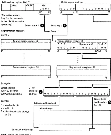
The relocation translator generates a physical address that allows any byte in storage to be addressed. Figure 2-1 shows an example of address translation. The letters in the following description correspond to the letters in Figure 2-1:
o
The active address key from the address key register selects a segmentation register stack. The address key pertains to the instruction being executed on the current priority level. Bit 12 is ignored in 3-bit mode.o
The five high-order bits (0-4) of the 16-bit address (generated for theinstruction being executed) select a segmentation register within the stack selected in description
O.
These bits define the logical segment.G
The physical address is generated. The high-order bits are from thesegmentation register; these bits specify the physical address of a 2K-byte segment of storage.
Segmentation Register Bit 13 - Valid Bit: When set to 1, this bit specifies that the contents of the segmentation register are valid; the segmentation register can be used to perform the translation. When bit 13 is a 0, the segmentation register cannot be used for translation (no access). If translation is attempted, a program-check interrupt occurs with invalid storage address set in the processor status word (PSW). (All valid bits are set to O's after power is switched on.)
Segmentation Register Bit 14 - Read-Only Bit: When set to 1, this bit specifies that the block is read-only. If an attempt is made to write into storage using a
Address key register (AK R)
I
ISK0 0 0
12 15
16-bit logical address
10 0 0 0 011 1 1 0 0 0 0 0 0
0 4 5 15
The active address key for this example
~ ~
,
~,---~~---~~is the ISK (instruction
space key) Select stack 1
e
Segmentation registersStack 0
Select reg 0
CD
Stack 1 Segmentation registera
1 - - - Segmentation register
~ _ _ _ _ _
Z Z Z Segment addr
Iv
R Za a a
0a a
1 1 0 0a
0a
1a a
o
o
Example:•
•
•
•
•
Segmentation register 31
15
15
o
3 1213 15o
•
•
•
•
...Segmentation register 31
15 Se!ect address 198,402 decimal 030702 hexadecimal 21-bit physical
address 8 1 0 0 0 1 1 0 0
a a
011 1 1 0 0 0a
0 0 1 01~==~====~,~,====~====~, ""'" ...
Legend: Select byte
(Storage address bus)
I
(address bits•
R
=
read-only bitV
=
valid bitZ = bits that should always
be a's
Select 2K-byte block Note: When the translator is disabled, address bits 0-15 only are used for main storage address selection_
[image:46.626.134.568.54.580.2]~
Figure 2-1. Address Translation Example
5-15) Main storage
I/O Storage Access Using the Relocation Translator
All storage access requests from I/O devices are translated by the same hardware that handles storage requests from the processor. The device control blocks (DCBs) must reside in the supervisor's address space; therefore, all I/O devices must use address key 0 to gain access to the DCBs and to store the individual residual status blocks. The address key of the process requiring a cycle-steal operation resides in a DCB. An I/O device presents this address key, along with a 16-bit logical address, to the relocation translator. This allows an I/O device to directly address the storage space for a particular process. The address key allows I/O storage protection to be established between address spaces, assuming that the supervisor ensures the integrity of the DCBs. In 4-bit translated mode, cycle-steal operations gain access to main storage through the I/O segmentation registers.
Status of Translator After Power Transitions and Resets
The translator is enabled by the Enable (EN) instruction, or by the PSW key of the programmer console, if installed. The translator is disabled by any of the
following:
Disable (DIS) instruction Power-on reset
Check Restart key on programmer console Initial program load (IPL)
System Reset key on programmer console.
All translator controls are reset when the translator is disabled. Notes:
1. A machine-check interrupt does not disable the translator.
Error-Recovery Considerations
Invalid Storage Address (ISA)
Protect Check
The invalid storage address bit (bit 1 of the PSW) is set to 1 by anyone of the following:
Storage access was attempted using a physical address greater than the physical storage size installed.
Storage access was attempted with bit 13 (valid bit) of the segmentation register set to 0. This signifies that the contents of the segmentation register are invalid.
The specific nature of the invalid storage address can be resolved as follows: Store the segmentation register following the program-check interrupt. Test the value of bit 13 in the selected segmentation register. When set to 1,
this bit specifies that the contents of the segmentation register are valid; the segmentation register can be used to perform the translation. When bit 13 is a
0, the segmentation register cannot be used for translation (no access). If
translation is attempted, a program-check interrupt occurs with invalid storage address set in the processor status word (PSW).
Ensure that the segment address does not exceed the limits of the physical processor storage installed.
When the translator is enabled, a program-check interrupt with protect check set in the PSW is caused by an attempt to write into storage, while in the problem state, using a segmentation register with bit 14 (read-only) set to 1.
Address Space Management
Active Address
Key
Cycle-steal devices have a cycle-steal address key specified in their device control block.
Anyone of the four address keys (ISK, OPIK, OP2K, or cycle-steal address key) may be used during a storage access as the active address key. The address key in use (active) depends on the type of operation being performed at a specific instant in time. The active address key defines storage access through a particular block of segmentation registers.
Each priority level in the processor has an associated address key register (AKR) that contains an equate-operand-spaces (EOS) bit and three address keys (OPIK, OP2K, and ISK). In 3-bit mode, three bits are used in each address key; in 4-bit mode, four bits are used in each address key.
3-bit mode address key register (AKR) 4-bit mode address key register (AKR)
Ixla
o
0alx
X
xlalx
X
xlalx
X
xl
Ixla
0alx
X X
xix
X X
xix
X X
xl
o
1 4 5 7 8 9 1112 13 15o
1 3 4 7 8 1112t
~ '-...-' '--.---'t
" - . . . - ' '- ~ I ,EOS OP1K OP2K ISK EOS OP1K OP2K
EOS Equate operand spaces. This bit, when set to 1, causes all data operands to use the OP2K address key. See "Equate Operand Spaces (EOS)" in this chapter.
~
ISK
OP1 K Operand 1 key_ These bits contain the binary-coded operand 1 address key, with bit 7 as the low-order bit.
OP2K Operand 2 key. These bits contain the binary-coded operand 2 address key, with bit 11 as the low-order bit.
ISK Instruction space key. These bits contain the binary-coded instruction-space address key, with bit 15 as the low-order bit.
15
I
Equate Operand Spaces (EOS)
The equate operand spaces bit (bit 0) in the address key register controls the use of the OPIK address key.
Address Space
When the relocation translator is enabled, an address key defines a specific address space where:
The address space is a range of logically contiguous storage.
The address space is accessible by the effective address without operating system intervention (the address space is not greater than 64K bytes).
All instruction fetches use the address space defined by the instruction space key (lSK). For storage-to-storage instructions, all reads and writes for data operand 1 use the address space defined by the OP 1 K, assuming that the EOS bit is a O. All other storage data accesses, reads, and writes use the address space defined by the OP2K, excluding branch and jump instructions.
Examples:
ISK=OPIK=OP2K. For instruction processing, all storage accesses occur
within the same address space.
ISK:;eOPIK,OPIK=OP2K. Instruction fetches occur in the ISK address
space. Data access occurs in the OP2K address space.
ISK:;eOPIK, OPIK:;eOP2K. Refer to Figure 2-2 for this example.
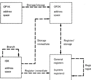
110 operations that access main storage also use an address key. Cycle-steal operations (read or write) use the cycle-steal address key specified within the device control block. An address key of a is used when the device fetches the device control block. Direct program control (DPC) operations that write data to storage use the OP2K address key.
Other defined uses of the address key register are as follows:
All indirect access for branching uses the ISK.
Effective-address generation occurs in the address space of the particular data operand. The appended words in the instruction are accessed by the ISK.
Storage access from the console is defined by the SAR address key.
Stop-on-address is based on the Stop On Address key when the translator is enabled.
OP1K
....
---
Storage/storage OP2K address addressspace space
r-I
I
I
I
Register/I
Storage immediate storageBranch
I
.---,
I
I
I
I
General - - .ISK _ _ .J registers
address
I
Register/space
- - - - -
Register immediate (systemI
register registers)_J
Assembler syntax for address spaces (see Appendix A)
ISK OP1K addr5 (reg)
OP2K Example instructions
Bits 12-15 ofAKR Bits 12-15 of AKR *Indirect addressing. Notes: addr4 (reg) AW MVFD MVBI B addr5,addr4 (reg), (reg) byte, reg longaddr*
1. OP1 K is only used for the source operand in storage-to-storage operations. 2. OP2K is used for storage data access in all other operations (excluding
branch/jump).
3. ISK (bits 13-15 of the AK R) is used for instruction fetch and branch/jump operations.
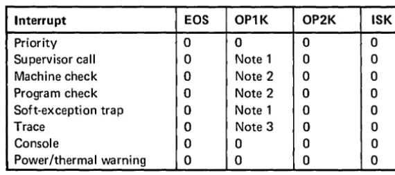
[image:51.627.181.497.53.328.2]Address Key Values After Interrupts
When priority or class interrupts occur, certain values are set in the address keys of the affected AKR. These values anticipate the address spaces that the programmer might need for interrupt processing. Figure 2-3 shows the resulting AKR values for each type of interrupt:
Interrupt EOS OP1K OP2K ISK
Priority 0 0 0 0
Supervisor call 0 Note 1 0 0
Machine check 0 Note 2 0 0
Program check 0 Note 2 0 0
Soft-exception trap 0 Note 1 0 0
Trace 0 Note 3 0 0
Console 0 0 0 0
Power/thermal warning 0 0 0 0
Notes:
[image:52.621.219.504.142.268.2]1. OP1 K is set to the precedi ng key contai ned in OP2K. 2. OP1 K is set to the last active processor address key. 3. OP1 K is set to the preceding key contained in the 15K.
Figure 2-3. Resulting AKR Values
All interrupt service routines reside in address space 0; therefore, the ISK and OP2K are set to O's when an interrupt occurs. Necessary information for processing a specific interrupt may reside in an address space other than O. The address key related to the particular interrupt is placed in OPIK. The OPIK is set in anticipation of a storage-to-storage move of information from the interrupting address space to address space O.
Chapter 3. Console
The basic console is a standard standard feature of the processor; the programmer console is an optional feature.
IPl Source
~~~
P,,,nary~
Alternite
[;-°1
Mode
CJ
o~
Auto IPl~
NorlNl
011 DI.gnostlc
LJLJLJLJOODD
LJLJLJ
~~.
DODD
l]
LJLJLJ
DODD
DLJOLJODDO
Basic console
Programmer console
The basic console is intended primarily for those systems that are totally dedicated to a particular application, where operator intervention is not needed during the execution of the application.
Basic Console
Each 4956 comes equipped with a basic console, which provides the following:
Power On/Off switch for the processor unit
IPL Source switch to select a primary or alternate IPL device
Load key for initial program load (IPL)
Mode switch to select: Auto IPL, Normal, or Diagnostic mode
• Load, Wait, Run, and Power On indicators.
o
Power On/Off: When this switch is set to the On position, power is applied to the processor unit. After all power levels are up, the Power On indicator is turned on. When this switch is set to the Off position, power is removed from the processor unit and the Power On indicator is turned off.e
IPL Source: This switch selects the I/O device to be used for program loading. In the Primary position, the device that was pre-wired as the primary IPL device is selected. In the Alternate position, the device that was pre-wired as the alternate IPL device is selected.CD
Load: Pressing this key causes a system reset, and the initial program load (IPL) sequence is started. The Load indicator is turned on and remains on until the IPL sequence is completed. When the IPL sequence is completed, instruction execution begins at location 0 on priority level O.e
Mode: This switch has the following positions:Auto IPL-In this position, an IPL is initiated after a successful power-on sequence. Bit 13 of the PSW is set to indicate to the software that an automatic IPL was performed. In this mode, Stop instructions are treated as no-ops.
Normal-In this position, Stop instructions are treated as no-ops.
Indicators
Programmer Console
o
Load: On when the machine is performing an initial program load (lPL).o
Wait: On when an instruction that exits the active level has been executed andno other priority interrupts or levels are pending.
e
Run: On when the machine is executing instructions.G
Power On: On when the proper power levels are available to the system.The programmer console is an optional feature that can be ordered with the 4956 or field-installed at a later date. The programmer console provides the following:
Start and stop of the processor.
Ability to display or alter any storage location. System reset.
Selection of anyone of the four interrupt levels for the purpose of displaying or altering data.
Displaying or altering of the storage address register (SAR), instruction address register (lAR), SAR address key register (AKR), stop-on-address address key register (AKR), level address key register (AKR), segmentation registers, console data buffer, or any general purpose register.
Displaying, but not altering, the level status register (LSR), current instruction address register (CIAR), op register, or processor status word (PSW). Note that the following bits of the PSW and LSR may be altered: PSW bit 14 (translator enabled), PSW bit 7 (4-bit mode), LSR bit 8 (supervisor state), and LSR bit 11 (summary mask).
Stop on address. Stop on error. Instruction stepping. Check restart.
Request for a console interrupt.
Check indicator. The Check indicator is a light emitting diode (LED) that lights when a machine check or program check class interrupt occurs. Lock console.
CE mode. The CE mode is used to display the error log.
Console Display
Run or Wait State
Stop State
When the processor is in run or wait state, the console data buffer is displayed in the data display indicators. An exception to this is when a Set Console Data Lights (SECON) instruction writes a message to the data lights and does not change the buffer. When the Data Buffer key is pressed, the console data buffer is again displayed in the indicators.
When the console data buffer is being displayed, the console data buffer and the display are changed by entering new data with the data entry keys.
When the processor enters stop state, the IAR is displayed in the data display indicators. Any system resource that has a corresponding select key on the console can be displayed. For example, the console data buffer can be displayed by pressing the Data Buffer key.
}
AConsole data buffer
IAR disp
LJLJLJDOODO
LJLJLJ
~~.
DODD
stop stat layed in e
LJLJ[J[JOODD
LJLJLJLJODDD
Power-On Reset
J
Displayable areas or
message from Set Con Data Lights instructio
sole
Indicators
o
Data Display: When the processor is in run state, the console data buffer is displayed in the data display indicators.The Set Console Data Lights (SECON) instruction ca