355
Improving Performance And Speed Of Flip-Flop Using
CBFF Technique
Keta Sriramachandram
1, V. Lakshmi Prasanna
21Assistant Professor, Department of ECE, Tirumala Engineering College, Narasaraopet(P.D), A.P 2ECE, Department of ECE, Tirumala Engineering College, Narasaraopet (P.D), A.P
[email protected],[email protected]
Abstract:In this paper, a novel low-power pulse-triggered flip-flop (FF) AND CONDITIONAL BOOSTING design is presented. A modified clock pulse generator is used for better pulse width and height. Simulations have been carried out using CMOS 45nm process technology. In recent years the ultra-low power application can be possible using sub threshold technology. Using the advantage of this technology the power consumption of these flip flops is minimized. Sub threshold circuit consume less power than strong inversion circuit at the same frequency. Design is done using TANNER 45nm technology. Experimental results in a 45-nm CMOS process indicated that the proposed flip-flop provided up to 70% lower latency with 70% less performance variability due to process variation compared with conventional pre charged differential flip-flops.
Recently, ultra-low power or energy systems are becoming more and more popular. These systems include implantable biomedical electronics, wireless sensor nodes, RFID tag, and many portable electronics. For these applications where minimal energy consumption is the primary design constraint, sub-threshold logic circuits are becoming increasingly accepted since they consume roughly an order of magnitude less power, compared with normal strong-inversion operation.
Keywords: Sub-threshold technology, flip-flop, Bootstrap.
1. INTRODUCTION:
Sub-threshold logic circuits are becoming increasingly accepted since they consume roughly an order of magnitude less power, compared with normal strong-inversion operation.
The reason for a growing importance of sub-threshold conduction is that the supply voltage has continually scaled down, both to reduce the dynamic power consumption of integrated and to keep electric fields inside small devices low, to maintain device reliability [7]. The amount of sub threshold conduction is set by the threshold voltage, which sits between ground and the supply voltage, and so has to be reduced along with the supply voltage. That reduction means less gate voltage swing below threshold to turn the device off, and as sub-threshold conduction varies exponentially with gate voltage. It becomes more and more significant as MOSFETs shrink in size.[2]
Flip flops are major building blocks in digital VLSI system. The applications areas where flip flops are majorly used are in registers, pipelines, state machines for sequencing data. Flip flop have direct impact on power consumption and speed of VLSI system. Flip flop and latches consume more power because of redundant transitions & clocking system which is included in it. Thus our aim is to design high performance and power efficient flip flop [1]. One of the challenging methods to design low power flip flop is to use sub threshold technology.
Power consumption of circuit depends on several factors such as data activity, frequency, supply voltage, capacitance leakage and short circuit current.[3]
356 scheme flip-flop have been changed in four different
manners. First, clock pulse generator is changed because of better pulse width and height of CLK pulse (CLKP) which drives three transistors P1, N3 and N8.CLKP is occurred only at the time of rising edge of the CLK otherwise it remains at logic “0”. Second, CLKP is applied in place of permanent
transistor logic. And fourth, to make faster switching and low power dissipation at intermediate node X, a negative bias scheme (Deng and Mo; 2015) is applied at the substrate (or body) terminal of transistor N1 and N2. All these changes make this flip flop a high performance and low powered flip flop device.[5].
Figure1:Conventational Flip-Flop Design
Initially, output Q is supposed to be “0”. It makes Qbfb at logic “1”. When CLK is“0”, then node X charges. If Data is at “1” and CLKP occurs, then is discharged via transistors N1, N2 and N8. And it charges output node Q through P2 transistor. But at the same time, a pass transistor N3 is also ON, it helps in charging output node quickly. A negative bias helps in node X discharging faster that generates through transistors N4 and N5 due to high logic at input Data. Data equals to “0”, then output discharges through pass transistor N3 at the input Data terminal with the occurrence of CLKP. It means, signal feed through scheme helps in charging and discharging of output q quickly.[boosting 2].
3. PROPOSED CBFF DESIGN:
For incorporating the conditional boosting into a pre charged differential flip-flop, four different scenarios
regarding input data capture should be considered, which are determined by the logic states of the input and output.[6]
These scenarios are as follows:
1) For a low output data, a high input data should trigger boosting for a fast capture of incoming data. 2) For a low output data, a low input data should trigger no boosting since the input need not be captured.
3) For a high output data, low input data should trigger boosting for a fast capture of incoming data. 4) For a high output data, a high input data should trigger no boosting.
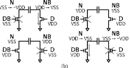
These scenarios can be embodied into a circuit topology using a single boosting capacitor by a combination of two operation principles. Output dependent presetting:[2]
357 The preset voltages of capacitor terminals N
and NB are made to be determined by outputs Q and
QB as shown in Fig. 2(a).
When Q=low, QB=high then MP7 is in on condition and MP6 is in off condition.MN8 is on. When Q=high, QB=low then MP7 is in off condition and MP6 is in on condition. So resulting in the
capacitor presetting given in right diagram in Fig. 1(a).
Input-dependent boosting: The boosting operations must be conditional to the input data given to the flip-flop.
Figure 2 (a): output data-dependent presetting and (b) input data-dependent boosting. Here the non-inverting input (D) is coupled
to NB through an nMOS transistor and the inverting input (DB) is coupled to N through another nMOS transistor, as shown in Fig. 2(b). Then, as one case in which a low data is stored in the flip-flop, resulting in the capacitor presetting given in the left diagram in Fig. 2(a), a high input allows NB to be pulled down to the ground, letting N being boosted toward –VDD due to capacitive coupling [upper left diagram in Fig.
2(b)]. Meanwhile, a low input allows N to be
connected to the ground, but since the node is already preset to VSS, there is no voltage change at NB, resulting in no boosting [lower left diagram in Fig. 2(b)]. Meanwhile, a high input allows NB to be
connected to the ground, but since the node is already preset to VSS, there is no voltage change at N, resulting in no boosting [upper right diagram in Fig. 2(b)].
4. CIRCUIT IMPLEMENTATION:
It is a combination of both pulse triggerd and symmetric latch circuit.
Pulse trigger diagram: In this pulse generator we use four inverters I1, I2, I4, and one transmission gate which is nothing but parallel combination of PMOS and NMOS along with an inverter I3.[Figure:3(a)].
Figure:3(a)
5. OPERATION OF PULSE
GENERATOR:
[image:3.612.205.417.242.353.2]358 Figure:3(b)
When clk pulse is high the pulse generator output is also high because the transmission gate is act as open switch and the width of pulse can be
determined by the latency of inverters I1,I2,I4.[refer figure:3(b)]
Figure:3(c)
Figure 3(a):pulse generator ,3(b):pulse generator when clk=low, 3(c):pulse generator when clk=high Symmetric latch:
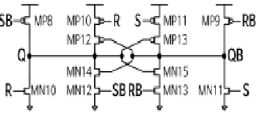
MN5/MN6/MN7 with boosting capacitor CBOOT are used to perform the input-dependent
boosting. MP8–MP13 andMN10–MN15 constitute the symmetric latch, as shown in Fig. 4.
Figure(4): Symmetric Latch
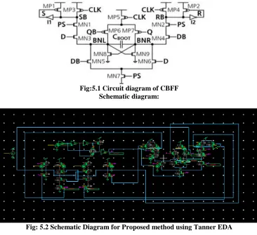
6. CIRCUIT IMPLEMENTATION: The structure of the proposed conditional-boosting flip-flop (CBFF) based on the concepts described in the previous section is shown in Fig(5.1). It consists of a conditional-boosting differential stage, a symmetric latch, and an explicit brief pulse generator. In the conditional boosting differential stage shown in Fig.MP5/MP6/MP7and MN8/MN9 are used to perform the output-dependent presetting. Unlike conventional pulse generators, the
[image:4.612.108.492.95.178.2] [image:4.612.84.519.247.337.2] [image:4.612.213.399.416.500.2]359 Fig:5.1 Circuit diagram of CBFF
[image:5.612.122.488.83.418.2]Schematic diagram:
Fig: 5.2 Schematic Diagram for Proposed method using Tanner EDA
[image:5.612.166.440.446.607.2]Simulation Waveforms:
Fig: 6 Simulation Waveforms
Fig (6) shows the timing diagram of the proposed flip-flop. To explain the operation, let us assume that initially Q is low when
CLK is low. Then, BNR is preset high due to the
turn-ON of MP5 asymmetric latchnd MP7, and BNL is
preset low due to the turn-ON of MN8 (output
dependent presetting). Now, when PS becomes high after the rising edge of CLK, BNL (BNR) will be connected to either SB (RB) or VSS depending on the input data. As shown in the first cycle in Fig. 3, since
D is high (different from Q), BNR is pulled down to
360
reduces the VTH and plays a role in further
increasing the driving capability. Moreover, the negatively boosted voltage transferred to SB allows the PMOS transistor in I1 and MP8 in the symmetric latch to have an increased driving capability, resulting in a fast pull-up of Q. Although the boosted
SB becomes briefly floating after the pull-down of
PS, any possible rise of SB due to leakage never causes output flipping, because MP13 and MN14 in the symmetric latch are fully OFF. Due to this condition, the circuit may not be adequate for operations at extremely low frequency. At the
cycle in Fig. 3, where D is maintained to be high (equal to Q). When PS becomes high after the rising
CLK edge, BNL is connected to SB, whereas BNR is connected to VSS. However, since BNL and BNR are already at high and low logic values, respectively, the boosting operation does not occur (input-dependent boosting), letting no output change. SB and RB are kept high by MP1 and MP2 to prevent any change by leakage. During the third cycle in Fig. 3 where Q is high and D is low, a negative boosting occurs at BNR
to get a fast pull down of Q.
7. RESULTS:
Simulation waveforms using Tanner EDA:
Fig(7): Simulation wave forms
361
8. CONCLUSION:
For aggressive voltage scaling down to the near threshold voltage region without severe performance degradation, a novel CBFF has been proposed. The evaluation in a 45-nm CMOS process indicates that the proposed flip-flop has smaller DQ latency, lower EDP, and less sensitivity to process variation.
REFERENCES:
[1] Yin-Tsung Hwang, Jin-Fa Lin, and Ming-Hwa Sheu, “Low-Power Pulse-Triggered Flip-Flop Design With Conditional Pulse-Enhancement Scheme,”. IEEE transactions on very large scale integration (vlsi) systems, vol. 20, no. 2, february 2012. [2] Ji-Hoon Park, Hyun-Seung Seo, and
Bai-Sun Kong, “Conditional-Boosting Flip-Flop for Near-Threshold Voltage Application,”
IEEE TRANSACTIONS ON VERY
LARGE SCALE INTEGRATION (VLSI) SYSTEMS 1063-8210 © 2016 IEEE. [3] bhawna vija1 and priyanka anand, “design
of pulse-triggered flip-flop for low power
applications using boost body-driven scheme,” Indian J.Sci.Res. 13 (1): 171-175, 2017.
[4] N. Kawai, “A fully static topologically-compressed 21-transistor flip-flop with 75% power saving,” IEEE J. Solid-State Circuits, vol. 49, no. 11, pp. 2526–2533, Nov. 2014. [5] bLin J.F., 2014. Low-power pulse-triggered
flip-flop design based on a signal feed-through scheme.
IEEE Transaction on VLSI Systems, 22:181- 185.
[6] J.-W. Kim, J.-S. Kim, and B.-S. Kong, “Low-voltage CMOS differential logic style with supply voltage approaching device threshold,” IEEE Trans. Circuits Syst. II, Exp. Briefs, vol. 59, no. 3, pp. 173–177, Mar. 2012.