Survey Paper of Performance Analysis of
Class EF2 Inverter and Rectifier for Wireless
Power Transfer Systems
Akshay Gapchup, Ashish Wadghule, Ankit Wani, Milind Baviskar
Student, Department of Electronics and Telecommunication, Savitribai Phule University, Pune, India
Student, Department of Electronics and Telecommunication, National Institute and Information Technology,
Aurangabad, India
ABSTRACT: Recent technologies such as wireless power transfer (WPT) and small-size radio-frequency plasma sources demand efficient, powerful, and multi megahertz switching resonant inverters. The EF2 inverters and rectifiers are designed to have high efficiency reduced second harmonic component and lower total harmonic distortion (THD), higher power-output capability, reduction in magnetic core requirements and operation at higher frequencies in rectification compared to other circuit topologies. This paper presents the overview of modeling and analysis of Class EF2 Inverter and Rectifier for Multi-megahertz for two 25W wireless power transfer (WPT) systems, one operating at 6.78MHz and the other at 27.12MHz.
KEYWORDS: Wireless Power Transfer, Class EF inverters, Class EF rectifiers
I. INTRODUCTION
The Wireless power transfer (WPT), wireless energy transmission, or electromagnetic power transfer is the transmission of electrical energy from a power source to an electrical load, such as an electrical power grid or a consuming device, without the use of discrete human-made conductors. Wireless power is a generic term that refers to a number of different power transmission technologies that use time-varying electric, magnetic, or electromagnetic fields. In wireless power transfer, a wireless transmitter connected to a power source conveys the field energy across an intervening space to one or more receivers, where it is converted back to an electrical current and then used. Wireless transmission is useful to power electrical devices in cases where interconnecting wires are inconvenient, hazardous, or are not possible.
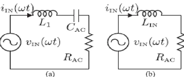
Figure.1. Circuit diagrams of the Class-EF2 inverter and rectifier
Class E network by connecting a series LC network, tuned to the second harmonic of the switching frequency, in parallel with the switch, referred to as class EF2. network. With this circuit can be designed at a higher operating dc voltage, which reduces the variation in the switch’s nonlinear output capacitance. Also Class-EF2 topology is that the switch’s drain voltage and the output load current does not contain a second-harmonic component, and therefore, has an improved EMI performance, whereas the Class-E topology contains a strong second-harmonic component, which may make it more difficult to meet EMI regulations. The Fig. 1 above shows the circuit diagrams of the Class-EF2 inverter and rectifier. The inductor can contribute to the majority of the losses in the circuit, especially when operating at frequencies in the megahertz range due to the losses associated with magnetic cores. In addition, the circulating dc current in the rectifier can cause the magnetic core to saturate, and therefore, the power that it can handle is limited.
II.LITERATURE SURVEY
The work in, for example, proposed a dual-frequency wireless power / wireless data system for implantable electronics. The two Tx coils, one for power and another for data, are placed orthogonal to each other in the transmitter in order to prevent interference between the two coils. Although this was effective for power and data transmission to one receiver, this cannot be applied to a multi-receiver use-case because the receiver would also need to be equipped with orthogonal coils, which is not feasible in most portable devices that have thin, planar geometries. Magnetic resonance coupling working at megahertz (MHz) is widely considered as a promising technology for the mid-range transfer of a medium amount of power. It is known that the soft-switching-based Class E rectifiers are suitable for high-frequency rectification, and thus potentially improve the overall efficiency of MHz wireless power transfer (WPT) systems. This paper reports new results on optimized parameter design of a MHz WPT system based on the analytical derivation of a Class E current-driven rectifier. 1.3 kW resonant power amplifier using a Gallium Nitride (GaN) device[3] at 13.56 MHz for wireless power transfer (WPT). The power amplifier driving the power transmitting coils is based on a Class
MHz switching frequency. These power GaN switching devices have low gate resistance RG and low capacitance CGS which greatly reduces the power requirements of the gate drive circuitry. The operation of traditional rectifiers such as half-wave and bridge rectifiers in wireless power transfer applications may be inefficient and can reduce the amount of power that is delivered to a load. An alternative is to use Class E resonant rectifiers that are known to operate efficiently at high resonant frequencies and at large input voltages. Class E rectifiers have a near sinusoidal input current which leads to an improved overall system performance and increased efficiency especially that of the transmitting coil driver. The concept of combining Class E and Class F or Class F-1 inverters was introduced by Kee in 2002 [12]. Since 2002, the research and contribution has been limited with fewer than ten journal papers published regarding Class EF and Class E/F inverters.
III.METHODOLOGY 1. Modeling and Analysis
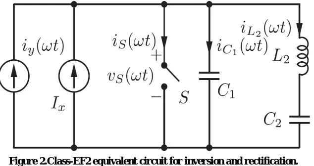
As shown in Fig.1 for both the EF2 inverter and rectification circuits, the resonant network of L2C2 tuned to resonate at the second harmonic of the circuits’ switching frequency. Both circuits shows dual nature, Both circuits are the dual of each other, that is the inverter circuit takes an input dc voltage (VIN ) and outputs ac current (Io ), and the rectifier circuit takes an input ac current (IIN ) and rectifies it into an output dc voltage (Vo ).The parameters annotations for voltage and current are described in Table 1 below. The analysis of equivalent circuit is shown in Fig. 2 can be based on following assumptions:
a) For both inversion and rectification the diode form an ideal switch for which ON resistance is zero, OFF resistance is infinity. The switching time is zero in inversion case whereas for rectification the forward voltage drop and reverse recovery time should be zero.
b) The inductance value L1 should be high such that the it keeps the input current IIN to dc for inversion and the input current iy to be sinusoidal with frequency same as switching frequency.
Figure 2.Class-EF2 equivalent circuit for inversion and rectification.
c) The loaded quality factor of the L3C3RL should be high to output current iy to be sinusoidal for inversion. For output voltage and current and voltage to be dc, the filter capacitor C3 should be high for rectification.
The shunt capacitance C1 is assumed to be constant and independent of its voltage for both inversion and rectification.
Table I Description Of The Voltage And Current Annotations
The current iy is sinusoidal and is given by
By applying the KCL at the switch’s drain node, the current in the switch is
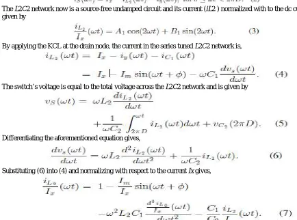
The L2C2 network now is a source-free undamped circuit and its current (iL2 ) normalized with to the dc current (Ix) is given by
By applying the KCL at the drain node, the current in the series tuned L2C2 network is,
The switch’s voltage is equal to the total voltage across the L2C2 network and is given by
Differentiating the aforementioned equation gives,
Substituting (6) into (4) and normalizing with respect to the current Ix gives,
The aforementioned equation is a linear nonhomogeneous second-order differential equation, which has the following general solution:
Inversion Rectification
S Mosfet Diode
where
and the coefficientsA2 andB2 are to be rom the determined based on the equation’s boundary conditions. The boundary conditions are determined current and voltage continuity conditions when the switch turns ON and OFF, which can be described by,
Using (9), the normalized current through capacitor C1 for the period 2πD ≤ ωt< 2π is,
The drain voltage for the period 2πD ≤ ωt<2π is,
whereτ is a dummy variable. The drain voltage can also be written as,
Where
By substituting (20) into (18), the normalized drain voltage with respect to the voltage Vxcan be written as,
Using (11), the normalized switch current with respect to the dc current Ix can be written as,
Figure. 3. Voltage and current waveforms for the Class-EF2 inverter (k = 0.867,D = 0.375).
2. Class EF2 Inversion
A. ANALYSIS
The analysis of EF2 is performed in cases of maximum power and frequency based on duty cycle and K. The maximum power operation can be described as
Voltage and Current Waveforms
Fig. 3 shows the voltage and current waveforms for the class EF2 inverter. the peak voltage and current stresses of the Class EF2 when k = 0.867 and D = 0.375 are
1) Input Resistance and Output Power:
and the input dc resistance seen by the source
Figure. 4. Comparison between the efficiencies of the Class-EF2 inverter operating at maximum cp [8] and the Class-E inverter.
where RL here represents the reflected load of the inductive link and the rectifier. Assuming all the power supplied by the source will be consumed in the reflected load, thus
The normalized output power is, therefore
B. COMPARISON WITH CLASS-E INVERTER
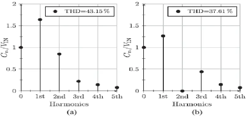
Harmonics:The Fourier analysis is performed for the harmonic investigation of drain waveforms. Using (21), the Fourier components of the drain voltage are
The first five components are used to calculate the THD as follows as there is so little power in the higher harmonics
The comparisons of harmonic contents of Class EF2 and E inverter are shown in Fig. 5 above. It reveals that the Class-E inverter has a strong second-harmonic component as compared to class Class-EF2 inverter therefore has a higher THD.
Figure. 5. Harmonic content of the switch’s voltage.
3. Class-Ef2 Rectification A. Analysis
The ZDS in rectification occurs at ωt= 2πD (iC1 (2πD) = 0, giving the following equation:
For the rectification circuit the output load current Io and k can be set as the independent parameters for diode operation and duty cycle need to be calculated. From (11), the ratio of the amplitude of input ac current Im to the output dc current Io can be written as
This ratio depends on load resistance. The duty cycle D as a function of normalized load current and k.
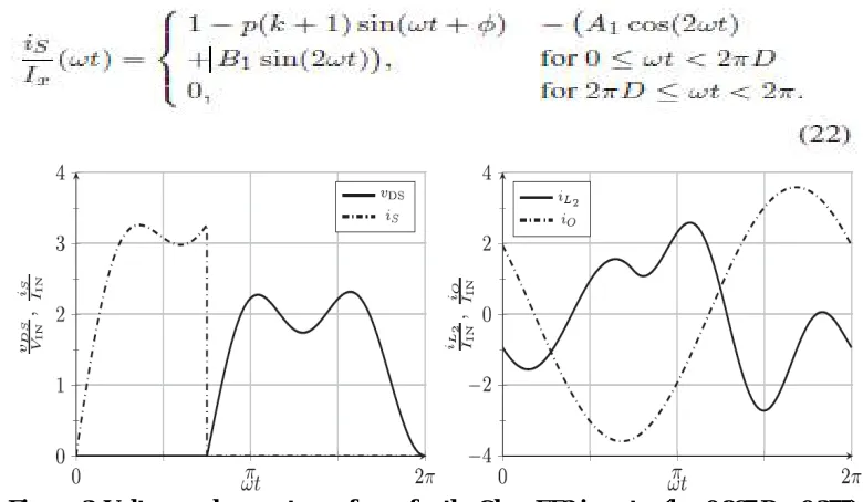
Voltage and Current Waveforms: By using the numerical solutions for A1 , A2 , B1 , B2 , p, and φ, the voltage and
current waveforms throughout the rectifier can be plotted for given values of Im Io and k. Fig. 7 shows the diode’s voltage and current waveforms and the current of inductor L2 for selected values of normalized load current and k.
Maximum Stresses and Power-Output Capability: Similar to the inversion case, the maximum cp is 0.13231, which occurs when k = 0.867 and Im Io = 3.5853 corresponding to the following voltage and current stresses:
Input Impedance: The equivalent circuit for calculating the input impedance is shown in Fig. 6 above. The fundamental Fourier component of the diode voltage is given by
Fig 6. Class-EF2 rectifier equivalent circuit and input impedance at the fundamental switching frequency. (a) equivalent circuit seen by vIN and L1 (b) input impedance cuircuit
IV. CONCLUSION
This paper presents the performance analysis of Class-EF2 inverter and a Class-EF2 rectifier topology for WPT systems that operate at multimegahertz frequencies. Detailed mathematical analysis was performed on the Class-EF2 topology to derive its component parameters for optimum switching conditions and other performance parameters such as voltage and current stresses, power-output capability, and harmonic content. Further will be presenting the design and implementation of Class EF2 inverter and rectifier.
REFERENCES
[1]D. Ahn and P. P. Mercier, “Wireless power transfer with concurrent 200 kHz and 6.78 MHz operation in a single transmitter device,” IEEE Trans. Power Electron., vol. 31, no. 7, pp. 5081–5029, Jul. 2016.
[2]M. Liu, M. Fu, and C. Ma, “Parameter design for a 6.78 MHz wireless power transfer system based on analytical derivation of Class E current driven rectifier,” IEEE Trans. Power Electron., vol. 31, no. 6, pp. 4280– 4291, Jun. 2016.
[3]J. Choi, D. Tsukiyama, Y. Tsuruda, and J. Rivas, “13.56 MHz 1.3 kW resonant converter with GaN FET for wireless power transfer,” in Proc. IEEE Wireless Power Transfer Conf., May 2015, pp. 1–4.
[4]S. Aldhaher, P. C.-K. Luk, and J. F. Whidborne, “Tuning Class E inverters applied in inductive links using saturable reactors,” IEEE Trans. Power Electron., vol. 29, no. 6, pp. 2969–2978, Jun. 2014.
[5]S. Aldhaher, P. C.-K. Luk, A. Bati, and J. F. Whidborne, “Wireless power transfer using Class E inverter with saturable dc-feed inductor,” IEEE Trans. Ind. Appl., vol. 50, no. 4, pp. 2710–2718, Jul. 2014.
[6]S. Aldhaher, P. C.-K. Luk, K. El KhamlichiDrissi, and J. F. Whidborne, “High-input-voltage high-frequency Class E rectifiers for resonant inductive links,” IEEE Trans. Power Electron., vol. 30, no. 3, pp. 1328–1335, Mar. 2015.
[7]T. Suetsugu and M. K. Kazimierczuk, “Comparison of Class E amplifier with nonlinear and linear shunt capacitance,” IEEE Trans. Circuits Syst. I, Fundam. Theory Appl., vol. 50, no. 8, pp. 1089–1097, Aug. 2003
[8]S. Aldhaher, D. C. Yates, and P. D. Mitcheson, “Modelling and analysis of Class EF and Class E/F inverters with series-tuned resonant networks,” IEEE Trans. Power Electron., vol. 31, no. 5, pp. 3415–3430, May 2016.
[9]A. Mediano and N. O. Sokal, “A Class-E RF power amplifier with a flat top transistor-voltage waveform,” IEEE Trans. Power Electron., vol. 28, no. 11, pp. 5215–5221, Nov. 2013.
[10]A. Grebennikov, “High-efficiency Class E/F lumped and transmission power amplifiers,” IEEE Trans. Microw. Theory Tech., vol. 59, no. 6, pp. 1579–1588, Jun. 2011.
[11]J. M. Rivas, Y. Han, O. Leitermann, A. D. Sagneri, and D. J. Perreault, “A high-frequency resonant inverter topology with low-voltage stress,” IEEE Trans. Power Electron., vol. 23, no. 4, pp. 1759–1771, Jul. 2008.
![Figure. 4. Comparison between the efficiencies of the Class-EF2 inverter operating at maximum cp [8] and the Class-E inverter](https://thumb-us.123doks.com/thumbv2/123dok_us/1613477.1200096/7.595.59.486.207.525/figure-comparison-efficiencies-class-inverter-operating-maximum-inverter.webp)