567 | P a g e
AREA AND POWER EFFICIENT CARRY SELECT
ADDER USING BRENT KUNG ARCHITECTURE
S.Durgadevi
1, Dr.S.Anbukarupusamy
2, Dr.N.Nandagopal
3Department of Electronics and Communication Engineering
Excel Engineering College,Komarapalayam,Namakkal-637303, Tamilnadu, (India)
ABSTRACT
Carry Select Adder (CSA) architectures are proposed using parallel prefix adders. Instead of using dual Ripple Carry Adders (RCA), parallel prefix adder Brent Kung (BK) adder is used to design Regular Linear CSA. Adders are the basic building blocks in digital integrated circuit based designs. They work by creating two signals for each bit position, based on whether a carry is propagated through from a less significant bit position, generated in that bit position, or killed in that bit position. Carry Select Adder is a compromise between RCA and CLA in term of area and delay. Delay of RCA is large therefore we have replaced it with parallel prefix adder which gives fast results. In this system, structures of 16-Bit Regular Linear Brent Kung CSA, Modified Linear BK CSA, Regular Square Root (SQRT) BK CSA and Modified SQRT BK CSA are designed. Power and delay of all these adder architectures are calculated at different input voltages.
Keywords-CSA RCA BK CLA (SORT).
I. INTRODUCTION
Very large scale integration (VLSI) is the process of creating an integrated circuit (IC), combining thousands of
transistors into a single chip. The strict limitation on power dissipation in any device must be met by the VLSI
chip designer without compromising in their computational requirements[1]. Reducing the total power
consumption in such system is important since it is desirable to maximize the run time with minimum
requirements on size, battery life and weight allocated to batteries. So the most important factor to consider
while designing any circuit is ‘low power’.
The term Prefix means, the outcome of the operation depends on the initial inputs. Parallel adders involve the
execution of an operation in parallel. This is done by segmentation into smaller pieces that are computed in
parallel[2]. It is fast because the processing is accomplished in a parallel fashion. The Operation can be any
568 | P a g e
II. ADDERS
The most basic arithmetic operation that digital computers can performs addition of binary digits. In electronics,
an adder or summer is a digital circuit that performs addition of numbers and is a fundamental building block in
VLSI[3]. Adders are used not only in the arithmetic logic units but also in digital signal processor or any other
kind of processors are used to calculate addresses and table indices Although adders can be constructed for
many numerical representation such as binary coded decimal or excess code, the most common adders operate
on binary numbers also in cases where two’s complement or other complement is being used to represent
negative numbers.
III. TYPES OF ADDERS
Adders can be broadly classified into two major categories namely,
• Serial Adders • Parallel Adders.
IV. SERIAL ADDER
A serial adder is used to add binary number in serial form the two binary numbers to be added serially are stored
in two shift registrar, b. Bits are added one pair at a time through a single full adder, Serial adder is done by a
flip flop and a full adder .The carry out of the full adder is transferred to a D flip flop. The output of this flip flop
is then used as the carry input for the next pair of significant bit. The sum bits from the S output of the full adder
could transfer to a third shift register. By shifting the sum into a while the bits of A are shifted out, it is
possible to use one register for storing both augends and sum of the bits .The serial input register b can be used
to transfer a new binary number the addend bits are shifted out during the addition.
V. PARALLEL ADDER
A binary parallel adder is digital circuits that adds two binary numbers in parallel form and produces the
arithmetic sum of those numbers in parallel form .the full adder connected in a chain output carry from each full
adder connected to the input carry of the next full adder in chain. The parallel adder classified into ripple carry
adder, carry look-ahead adder[4].
5.1 Ripple Carry Adder (RCA)
A RCA is simply several full adder is connected in a series so that the carry must propagate through every full
adder before addition is complete RCA require the least amount of hardware of all adders ,but they are slowest.
569 | P a g e
Fig.1.4.1(a) Block Diagram Of Ripple Carry Adder (RCA)The interconnection of four full adder circuits provides a 4-bit parallel adder. The augend bits of ‘A’ and addend
bits of ‘B’ are designated by subscript numbers from right to left, with subscript 1 denoting the lower order bit.
The carries are connected in a chain through the full adders. The input carry to the adder is C in and the output
carry is Co. The S outputs generate the required sum bits .When the 4-bit full adder circuit is enclosed within an
IC package, it has four terminals for augend bits, four terminals for the addend bits, four terminals for the sum
bits and two terminals for the input and output carries. An n-bit parallel adder requires n full adder. The output
carry from one packages must be connected to the input carry of the one with the next higher-order bits the
4-bits full adder.
The 4-bit parallel adder in figure 1.1(a) sum (S1) and carry out (C1) bits given by full adder 1 are not valid
,until after the propagation delay of full adder1.similarly ,the sum S2 and carry out(C2)bits given by full adder2
are not valid until after the cumulative propagation delay of two adder , and so on.
At each stage , the sum bit is not valid until after the carry bits in all the preceding stages are valid in effect
,carry bits must propagate or ripple carry through all stages before the most significant sum bit is valid .Thus,
the total sum the parallel output is not valid after the cumulative delay of all the adders. The sum and carry-out
of the adder can be calculated as,
Sum=A!B!C
Carry=(A&B)|(B&C)|(A&C)
Propagation delay (RCA)=(N-1) tRCAcarry + N.tRCAsum
Where,
tRCAcarry - the delay for the carryout
tRCA sum - the delay for the sum
The parallel adder in which the carry out of each full adder is the carry-in to the next most significant adder is
called RCA[6]. The greater the numbers or bits that a ripple carry adder must add , the greater the time
required for it to perform a valid addition .If two numbers are added such that no carries occur between stages
then the add time is simply the propagation time throughs a single full adder.RCA is faster than serial adder and
570 | P a g e
5.2 Carry Look Ahead Adder (CLA)
A CLA is a type of adder used in digital logic .A CLA improves speed by reducing the amount of time required
to determine carry bits.
Fig .1.4.2(B)Block Diagram Of Carry Look AheadAadder (CLA)
Carry look-ahead logic uses the concepts of generating and propagating carries. Although in the context of a
carry look-ahead adder, it is most natural to think of generating and propagating in the context of binary
addition, the concepts can be used more generally than this. In the descriptions below, the word digit can be
replaced by bit when referring to binary addition.
The addition of two 1-digit inputs a and b is said to generate if the addition will always carry, regardless of
whether there is an input carry equivalently, regardless of whether any less significant digits in the sum carry.
For example, in the decimal addition 52 + 67, the addition of the tens digits 5 and 6 generates because the result
carries to the hundreds digit regardless of whether the ones digit carries. The delay is linearly dependent on N,
(length of the adder) and the carryout signal contributes largely to the delay. Circuit level modifications that
reduce carryout can greatly speeds up the addition operation .The carryout can be calculated with generate,
propagate, and carry in. The signals g and p are not dependent on carry in, and can be calculated as soon as the
input operands arrive. Weinberger and smith invented the CLA. The main idea behind CLA addition is to
generate all incoming carries in parallel and avoid unnecessary delay for carry propagation from the stage of the
adder where it has been generated. Very short carry propagate, that is independent of word length
Carry look ahead depends on two things:
• Calculating, for each digit position, whether that position is going to propagate a carry if one comes in from
the right.
• Combining these calculated values to be able to deduce quickly whether, for each group of digits, that group
is going to propagate a carry that comes in from the right.
The net effect is that the carries start by propagating slowly through each 4-bit group, just as in a ripple-carry
system, but then move 4 times as fast, leaping from one look ahead carry unit to the next[5]. Finally, within each
group that receives a carry, the carry propagates slowly within the digits in that group.
The more bits in a group, the more complex the look ahead carry logic becomes, and the more time is spent on
the slow roads in each group rather than on the fast road between the groups provided by the look ahead carry
logic. On the other hand, the fewer bits there are in a group, the more groups have to be traversed to get from
571 | P a g e
Deciding the group size to be governed by look ahead carry logic requires a detailed analysis of gate andpropagation delays for the particular technology being used.
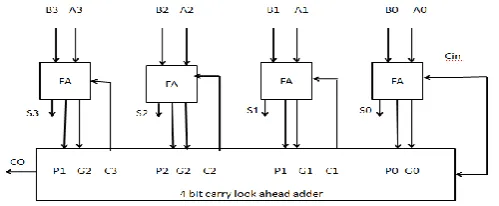
5.3. Carry Select Adder (CSA)
CSA is particular way to implement an adder in electronics device, which is a logic element that computers the
(n+1)-bit sum of two n-bit numbers. The CSA is simple but very
Fast
.
Fig.1.4(c) Block Diagram Of Carry Select Adder (CSLA)
The carry select adder includes in the category of conditional adder .Here sum and carry are calculated by
assuming input carry as 0 and 1 separately which are fed to a multiplexer whose select signal is the carry out of
previous stage. The conventional carry select consists of k/2 bit adder for the upper half most significant bit’s
(MSB) two k bit adders. This technique of dividing adder into stages increases the area utilization but also
speeds up the addition operation. The block diagram of conventional k CSA adder is shown in figure1.4(c).The
CLA is used in many computational systems to alleviate the problem of carry propagation delay by
independently generating multiple carries and then select a carry to generate the sum.CLA is parallel
computation reduced to carry propagate length and this type adder is very fast calculate all the inputs
simultaneously. Draw of CSA is more costly than other adder and designing is complex.
Carry select adderis a particular way to implement an adder, which is a logic element that computes the
(n+1)-bit sum of two -bit numbers. The carry-select adder is simple but rather fast, having a gate level depth of (n).
The carry-select adder generally consists of two ripple carry adders and a multiplexer. Adding two n-bit
numbers with a carry-select adder is done with two adders therefore two ripple carry adders in order to perform
the calculation twice, one time with the assumption of the carry being zero and the other assuming one. After the
two results are calculated, the correct sum, as well as the correct carry, is then selected with the multiplexer once
the correct carry is known.
The number of bits in each carry select block can be uniform, or variable. In the uniform case, the optimal delay
occurs for a block size. When variable, the block size should have a delay, from addition inputs A and B to the
carry out, equal to that of the multiplexer chain leading into it, so that the carry out is calculated just in time. The
delay is derived from uniform sizing, where the ideal number of full-adder elements per block is equal to the
572 | P a g e
A conditional sum adders a recursive structure based on the carry-select adder. In the conditional sum adder, theMUX level chooses between two bit inputs that are themselves built as conditional-sum adder[7]. The bottom
level of the tree consists of pairs of 2-bit adders (1 half adder and 3 full adders) plus 2 single-bit multiplexers.
1.4.(D) Comparsion Of Parameter Adder
1.4(E) Bar Chart Of Parameter Adder
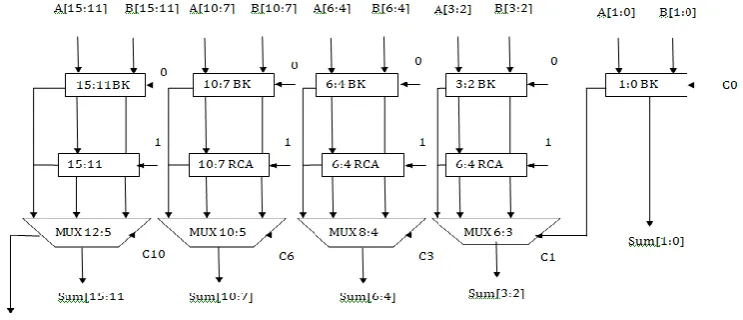
VI. 16-BIT LINEAR MODIFIED BK CSA
Regular Linear Brent Kung Carry Select Adder uses single Ripple Carry Adder (RCA) for Cin=O and Brent
Kung adder[8] for Cin=l and is therefore area-consuming. So, different add-one schemes like Binary to Excess-
1 Converter (BEC) have been introduced. Using BEC, Regular Linear BK CSA is modified in order to obtain a
reduced area and power consumption. Binary to Excess-l converter is used to add 1 to the input numbers[9]. So,
here Brent Kung adder with Cin=1 will be replaced by BEC because it require less number of logic gate for its
implementation so the area of circuit is less. Linear Modified BK CSA is designed using Brent Kung adder for
Cin=O and Binary to Excess-l Converter for Cin=l in order to reduce the area and power consumption with
573 | P a g e
Fig 4.1(a) Block Diagram Of 16-Bit Linear Modified BK CSATo replace the N-bit Brent Kung adder, aN+l bit BEC is required. The importance of BEC logic comes from the
large silicon area reduction when designing Linear Modified BK CSA for large number of bits.
VII. REGULAR SQUARE ROOT BRENT KUNG CARRY SELECT ADDER
Regular Linear Brent Kung Carry Select Adder consumes large area and to reduce its area a new design of adder
is used i.e. Regular Square Root Brent Kung Carry Select Adder. Regular Square Root BK CSA has 5 groups of
different size RCA for Cin=1 and MUX. High area usage and high time delay are the two main disadvantages of
Linear Carry Select Adder. These disadvantages of linear carry select adder can be rectified by SQRT CSA. It is
an improved version of linear CSA. The time delay of the linear adder can decrease, by having one more input
into each set of adders than in the previous set. This is called a Square Root Carry Select Adder[2].
574 | P a g e
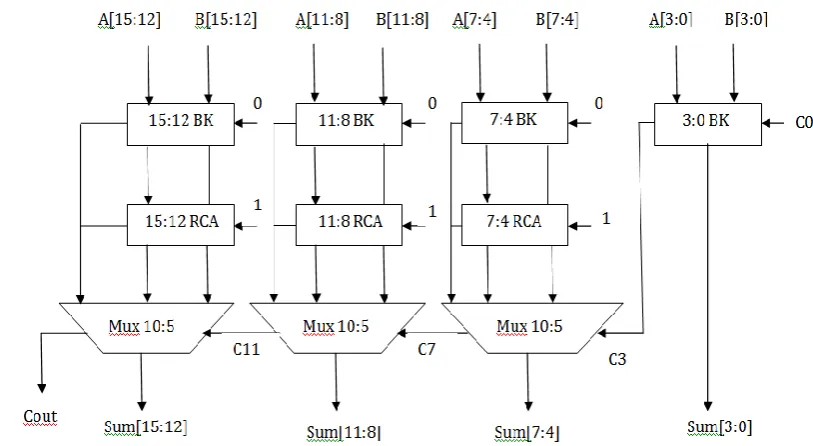
VII. MODIFIED SQUARE ROOT BRENT KUNG CARRY SELECT ADDER
Modified Square Root Brent Kung Carry Select Adder has been designed using Brent Kung adder for Cin=O
and BEC for Cin=l and then there is a multiplexer stage. It has 5 groups of different size Brent Kung adder and
Binary to Excess-l Converter (BEC). BEC is used to add 1 to the input numbers. Less number of logic gates are
used to design BEC as compared to RCA therefore it consumes less area.
Figure 4.4(a) Regular Linear Brent Kung Carry Select Adder
Binary excess converter:
By giving 4 inputs (B0 B1 B2 B3) the outputs obtained are (X0 X1 X2 X3) here we use 2 wire lines and for an
575 | P a g e
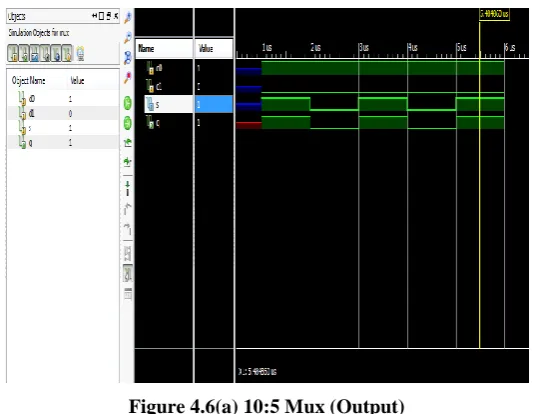
10:5 Mux:Figure 4.6(a) 10:5 Mux (Output)
In multiplexer we will give 2 inputs (do, d1) and there will be an single output (q).we will use single selection
line whose when it is 0 1st output will be displayed when it is 1 the another one will be displayed
Brent Kung adder:
Figure 4.7 (a) Brent Kung adder (output)
In this there will be 8 inputs (a [0:7], [0:7] b) and equal number of outputs. We use 37 wires in this. To
produce the output we will use generate and propagate operations[8].
576 | P a g e
4.9 Bar Chart Comparisons of parallel prefix adderVIII. CONCLUSION
In this work, a Modified Square Root BK Carry Select Adder is proposed which is designed using single Brent
kung adder and Binary to Excess-l Converter instead of using single Brent kung adder for C in=O and Ripple
Carry Adder for C in=l in order to reduce the delay and power consumption of the circuit. Here, the adder
architectures like Regular Linear BK CSA, Modified Linear BK CSA, Regular SQRT BK CSA and Modified
SQRT BK CSA are designed for 16-Bit wordsize only. This work can be extended for higher number of bits
also. By using parallel prefix adder, delay and power consumption of different adder architectures is reduced.
REFERENCES
[1] K. Saranya, "Low Power and Area-Efficient Carry Select Adder",International Journal of Soft Computing
and Engineering, Vol.-2, Issue-6January 2013.
[2] Yajaun He, Chip-Hong Chang, and JiangminGu, "An area efficient 64- Bit square Root carry-select adder
for low power Applications, " in Proc. IEEE International Symposium Circuits and Systems, vol. 4, pp.
4082- 4085,2005.
[3] M. Snir, "Depth-Size Trade-Offs for Parallel Prefix Computation", Journal of Algorithms, Vo!.7, Issue-2,
pp.185-201, June 1986.
[4] David Jeff Jackson and Sidney Joel Hannah, "Modelling and Comparison of Adder Designs with Verilog
HDL", 25th South-eastern Symposium on System Theory, pp.406, March 1993.
[5] Belle W.Y. Wei and Clark D. Thompson, "Area-Time Optimal Adder Design", IEEE transactions on
Computers, vo!.39, pp. 666-675, May1990.
[6] Y. Choi, "Parallel Prefix Adder Design", Proc. 17th IEEE Symposium on Computer Arithmetic, pp. 90-98,
27th June 2005.
[7] J. M. Rabaey, "Digital Integrated Circuits- A Design Perspective", New Jersey, Prentice-Hall, 2001.
[8] R. Brent and H. Kung, "A regular layout for parallel adders", IEEE Transaction on Computers, vol. C-31,n
577 | P a g e
[9] AdilakshmiSiliveru, M. Bharathi, "Design of Kogge-Stone and BrentKung adders using Degenerate PassTransistor Logic", International Journal of Emerging Science and Engineering, Vol.-I, Issue-4, February
2013.
[I0] ShivaniParmar and Karat Pal Singh," Design of High Speed Hybrid Carry Select Adder", IEEE's 3rd
International Advance Computing Conference (IACC) Ghaziabad, ISBN: 978-1-4673-4527-9, 22-23