Available online: https://edupediapublications.org/journals/index.php/IJR/ P a g e | 3437
ABSTRACT: Digital multipliers can be included among the highly significant arithmetic functional units. High speed and low power consumption is one of the significant objectives of design in integrated circuits. As multipliers are widely utilized in circuits, the multipliers must be efficiently designed. Here, a design of multiplier with aging aware is existed with adaptive hold logic (AHL). Complex numbers multiplication is a arithmetic operation to be performed with less power consumption and high speed in systems which having high performance such as wireless communications. Hence, in this paper, two possible architectures are proposed. The architecture of proposed multiplier with minimum path delay is used in the implementation of complex multiplier. The architectures for the three multiplier solution and four multiplier solution of complex multiplier for complex numbers multiplication are coded and implemented through Xilinx ISE.
Keywords: Proposed multiplier, complex multiplier, Adaptive hold logic (AHL)
I.INTRODUCTION
Multipliers are a fundamental component of a processor since multiplying operation is necessarily performed more than once in every logical computing process. The quick and low power multipliers are used in minor size wireless sensor systems and numerous other DSP (Digital Signal Processing) applications [5]. Distinctive computer arithmetic techniques can be utilized to execute any digital multiplier. Among these most techniques include
processing a partial products, and
afterward adding up the partial products
together. Most of the minicomputers didn’t
have instructions for multiplication
purpose be that as it may,
Mainframe computers did have
instructions for multiplication [9], and however they did a few sorts of shifting and adding operations as a "multiply routine". Microprocessors likewise had no multiplication instruction [4]. At that point the Motorola 6809, presented in 1978, was among first microprocessors with a separate part of hardware for multiply instructions.
Multipliers are essential to implement the computationally intensive digital signal processing units such as discrete Fourier transform (DFT) and multiply accumulate (MAC). The speed of the processor is majorly determined by the processing speed of multipliers [1] [2]. Hence, parallel and reconfigurable Field Programmable Gate Array (FPGA) based hardware architectures are needed to be designed. Moreover, due to the complex nature of wireless channel, complex multiplication process recently has received a significant importance in the area of broad band wireless communication techniques. In this context, a large number of complex multipliers are essential to implement the hardware modules [3]. Tiwari et al. has shown that the multiplier is faster than the
array multiplier. However, complex
Design a High Speed and Area Efficient Multiplier Using
Adiabatic Logic
1 VINJAMURI VENKATA ARJUN, 2 BHADINENI RAJESH
Available online: https://edupediapublications.org/journals/index.php/IJR/ P a g e | 3438 multiplication process has not been
addressed in this work.
High speed ASIC design of a complex multiplier is implemented using the four real multipliers solution. However, FPGA implementation of a complex multiplier has not been discussed. Further, path delay
analysis of proposed multiplier
architectures [6], which will enable to choose an architecture with minimum delay is lacking in the literature.
Hence, in this paper, we presented two possible architectures of a multiplier. Based on the path delay analysis of the two architectures, an expression for path delay of an N x N multiplier with path delay
architecture which is minimum is
developed. Next, we implemented a complex multiplier using three and four multipliers solutions [8].
II. EXISTED SYSTEM
A. 4 × 4 normal Array Multiplier: Low
power consumption is also suggested in a row-by-pass multiplier to decrease the power corresponding to the AOS activity as shown in Figure 2. The process of the row multiplier to go through at low power is similar to the multiplier to the low power column, but the multiplexer selector and the tristate gate uses multiplication.
Fig. 1: 4 × 4 normal AM.
B. Row- by passing multiplier: Every
source is linked to FA over a tristate gate. Assuming inputs as 11112 * 10012, both entries in the 1st and 2nd row has been 0 for FA. Since b1 seen as 0, multiplexers of the 1st line as aib0 bit of selected addition and bit 0 as selected transport. Voices are diverted to FA in the second row, and close off the saddle paths in the FA. Therefore, no switching activity takes place in a row FA; In return, energy intake is decreased. Similarly, since b2 has been 0, In this manner, no exchanging movement happens in 2nd row FA.
Fig. 2: Row bypassing multiplier
Be that as it may, FAs must be dynamic in the third line in light of the fact that b3 as multiplexer zero selector to settle on the yield of the FA and AI can likewise be utilized as a tristate gate selector to clear FA i/p way.
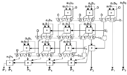
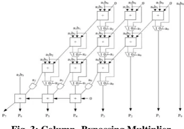
C. Column-by passing multiplier: A
Available online: https://edupediapublications.org/journals/index.php/IJR/ P a g e | 3439 aggregate of bits drops and 2) the convey
bit towards the lower left bay of the FA. The final line is a ripple aggregate for carry producing. FAS in AM are constantly dynamic paying little respect to the contributions, a low-power design is the column bypass multiplier where FA
operations are deactivated if the
corresponding multiplying bit is 0. Fig. 3 shows a4 × 4 columns by pass multiplier. Assuming that the sources are 10102 * 11112, it can be seen by the FA that in the 1st and 3rd diagonals, 2 of the 3 input bits are 0: the convey bits of upper FA and the partisan multiplication AIBI.
Fig. 3: Column- Bypassing Multiplier
The existed architecture is of aging-aware reliable multiplier. It sums up the whole architecture and the functions of each component.
III. EXISTED ARCHITECTURE
The aging aware multiplier design, consists of two m--bit source i/p (m has non- negative value), one with 2m-- bit
yield, one column- or row-bypass
multiplier, 2m with one-bit Razor flip-flop and AHL as illustrated in Fig 4.
When patterns of the input arrive, the execution of column bypassing multiplier and the AHL circuit is performed
simultaneously. Depends on the number of 0’s in the md , the AHL circuit decides that 1 or 2 cycles are required for the input patterns. If the input pattern need two cycles for completion, AHL will output 0 for disabling the flip-flops clock signal. Otherwise, AHL will 1 as output for the
normal operations. When the row
bypassing multiplier or column bypassing multiplier operation is performed, the result will be provided to the Razor flip-flop.
If timing infraction occurs, it means the
cycle period is not long enough for the present operation for completion and that the execution result of the multiplier is in correct. Thus, the Razor flip-flops will produce output an error for informing the system that the current operation needs to be re-executed by utilizing two cycles to ensure the operation is correct. In this condition, the extra cycles of re-execution which are generated by timing infraction
incurs to overall average latency.
Available online: https://edupediapublications.org/journals/index.php/IJR/ P a g e | 3440
Fig. 4: Existed Architecture
IV. PROPOSED SYSTEM
A. 2 x 2 bit proposed Multiplier: The 2 x
2 bit proposed multiplier can be
implemented by utilizing two half adders and four two input AND gates as shown Fig.5. The c2 s2 s1 s0 are the product bits.
Fig.5 : Block diagram of 2x 2 bit proposed Multiplier
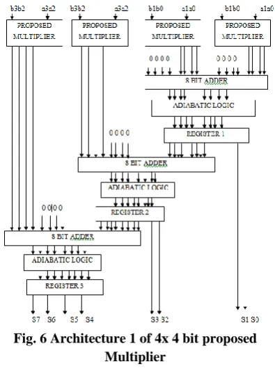
B. 4 x 4 bit proposed Multiplier:
Consider two 4 bit binary numbers ‘a3, a2,
a1, a0’ and ‘b3, b2, b1, b0’. Divide the multiplicand into two parts each contains two bits as a3 a2 and a1 a0. similarly, divide the multiplier into two parts as b3 b2 and b1 b0. Taking two bits at a time and utilizing 2 x 2 bit proposed multiplier, two possible architectures for 4x4 bit proposed multiplier utilizing four 2x2 bit proposed multipliers are shown in Figs. 5
and 6 respectively. The final product is s7 s6 s5 s4 s3 s2 s1 s0. The architecture 1 shown in Fig. 6 uses 8 bit adders whereas the architecture 2 shown in Fig.7 uses 4 bit ripple carry adders.
Fig. 6 Architecture 1 of 4x 4 bit proposed Multiplier
Fig. 7 Architecture 2 of 4x 4 bit proposed Multiplier
Available online: https://edupediapublications.org/journals/index.php/IJR/ P a g e | 3441
Fig 8. RTL Schematic
Fig 9. Technology Schematic
Fig 10. Output Waveform
VI. CONCLUSION
This paper has presented a design of high efficient proposed multiplier. The path
delay analysis of two possible
architectures of the proposed multiplier is performed and obtained an expression for path delay of N bit proposed multiplier with minimum delay architecture. Further,
the architectures of four real multipliers solution and three real multipliers solution are presented for proposed complex multiplier. The two solutions of complex multiplier are implemented using VHDL. From the implementation results, it is observed that the proposed complex multiplier is more efficient taking less path delay and less power consumption.
VII. REFERENCES
[1] P. K. Saha, A. Banerjee, and A. Dandapat, "High Speed Low Power Complex Multiplier Design Using Parallel Adders and Subtractors," International Journal on Electronic and Electrical Engineering, (IJEEE), vol 07, no. II, pp 38-46, Dec. 2009
[2] K.Hwang, Computer Arithmetic:
Principles, Architecture and Design. New York: John Wiley & Sons, 1979.
[3] A. Calimera, E. Macii, and M. Poncino, “Design techniqures for NBTI
tolerant power-gating architecture,” IEEE
Trans. Circuits Syst., Exp.Briefs, vol. 59, no. 4, pp. 249–253, Apr. 2012.
[4]Y.-S. Su, D.-C. Wang, S.-C. Chang, and
M. Marek-Sadowska, “Performance”
optimization using variable-latency design
style,” IEEE Trans. Very Large Scale
Integr. (VLSI) Syst., vol. 19, no. 10, pp. 1874–1883, Oct. 2011.
[5]N. V. Mujadiya, “Instruction scheduling on variable latency functional units of VLIW processors,” in Proc. ACM/IEEE ISED, Dec. 2011, pp. 307–312.
Available online: https://edupediapublications.org/journals/index.php/IJR/ P a g e | 3442 [6]B. C. Paul, K. Kang, H. Kufluoglu, M.
A. Alam, and K. Roy, “Negative bias temperature instability: Estimation and
design for improved reliability of
nanoscale circuit,” IEEE Trans. Comput.-Aided Des. Integr. Circuits Syst., vol. 26, no. 4, pp. 743–751, Apr. 2007.
[7] Y. Cao. (2013). Predictive Technology
Model (PTM) and NBTI Model [Online].
Available: http://www.eas.asu.edu/∼ptm
[8] S. Zafaret al., “A comparative study of
NBTI and PBTI (charge trapping) in SiO2/HfO2 stacks with FUSI, TiN, Re
gates,” in Proc.IEEESymp. VLSI Technol.
Dig. Tech. Papers, 2006, pp. 23–25.
[9] A. Calimera, E. Macii, and M.
Poncino, “Design techniqures for
NBTItolerant power-gating architecture,” IEEE Trans. Circuits Syst., Exp. Briefs, vol. 59, no. 4, pp. 249–253, Apr. 2012. [10] K.-C. Wu and D. Marculescu, “Joint logic restructuring and pin reordering
against NBTI-induced performance
degradation,” in Proc. DATE, 2009, pp.
75–80.
[11] Y. Lee and T. Kim, “A fine-grained technique of NBTI-aware voltage scaling and body biasing for standard cell based
designs,” in Proc. ASPDAC, 2011, pp.
603–608.
[12] M. Basoglu, M. Orshansky, and M. Erez, “NBTI-aware DVFS: A new approach to saving energy and increasing
processor lifetime,” in Proc. ACM/IEEE
ISLPED, Aug. 2010, pp. 253–258.
[13] K.-C. Wu and D. Marculescu,
“Aging-aware timing analysis and
optimization considering path
sensitization,” in Proc. DATE, 2011, pp.
1–6.
[14] K. Du, P. Varman, and K. Mohanram, “High performance reliable variable
latency carry select addition,” in Proc.
DATE, 2012, pp. 1257–1262.
[15] A. K. Verma, P. Brisk, and P. Ienne, “Variable latency speculative addition: A new paradigm for arithmetic circuit
design,” in Proc. DATE, 2008, pp. 1250–
1255.
[16] D. Baneres, J. Cortadella, and M. Kishinevsky, “Variable-latency design by
function speculation,” in Proc. DATE,