Worcester Polytechnic Institute
Digital WPI
Major Qualifying Projects (All Years)
Major Qualifying Projects
April 2016
Accelerating Augmented Reality Video Processing
with FPGAs
Andrew James Weiler
Worcester Polytechnic Institute
Anthony Daniel Dresser
Worcester Polytechnic Institute
Lukas Laurence Hunker
Worcester Polytechnic Institute
Follow this and additional works at:
https://digitalcommons.wpi.edu/mqp-all
This Unrestricted is brought to you for free and open access by the Major Qualifying Projects at Digital WPI. It has been accepted for inclusion in Major Qualifying Projects (All Years) by an authorized administrator of Digital WPI. For more information, please [email protected].
Repository Citation
Weiler, A. J., Dresser, A. D., & Hunker, L. L. (2016).Accelerating Augmented Reality Video Processing with FPGAs. Retrieved from
Accelerating Augmented
Reality Video Processing with
FPGAs
4/27/2016
Anthony Dresser, Lukas Hunker, Andrew Weiler
Advisors: Professor James Duckworth, Professor Michael Ciaraldi
A Major Qualifying Project
Submitted to the Faculty of
Worcester Polytechnic Institute
in partial fulfillment of the requirements for the
Degree of Bachelor of Science
This report represents work of WPI undergraduate students submitted to the faculty as evidence of a
degree requirement. WPI routinely publishes these reports on its web site without editorial or peer
Abstract
This project implemented a system for performing Augmented Reality on a Xilinx Zync FPGA. Augmented and virtual reality is a growing field currently dominated by desktop computer based solutions, and FPGAs offer unique advantages in latency, performance, bandwidth, and portability over more traditional solutions. The parallel nature of FPGAs also create a favorable platform for common types of video processing and machine vision algorithms. The project uses two OV7670 cameras mounted on the front of an Oculus Rift DK2. A video pipeline is designed around an Avnet ZedBoard, which has a Zynq 7020 SoC/FPGA. The system aimed to highlight moving objects in front of the user.
Executive Summary
Virtual and augmented reality are quickly growing fields, with many companies bringing unique hard-ware and softhard-ware solutions to market each quarter. Presently, these solutions generally rely on a desktop computing platform to perform their video processing and video rendering. While it is easy to develop on these platforms due to their abundant performance, several issues arise that are generally discounted: cost, portability, power consumption, real time performance, and latency. This project develops a Field Programmable Gate Array (FPGA) and System On a Chip (SOC) based solution to address these issues while simultaneously attempting to achieve the capabilities of the desktop solutions. To achieve this goal, the project performs object tracking by highlighting objects that moved in front of the user. Object tracking was chosen because it is a building block that can be used in other applications, and demonstrates the potential of the system. Cost compares at $500 for FPGAs versus over $1000 for desktop computers. Power consumption can be drastically reduced from 500-600 watts to under 10 watts for many video processes, allowing the platform to be portable and battery powered. Video processes on desktop platform generally have a baseline latency of 11-17ms due to frame buffers, but FPGAs can run a video processing pipeline end to end in the micro second domain. These statistics make FPGAs a clear candidate for augmented reality.
The developed augmented reality solution uses two OV7670 cameras mounted on the front of an Oculus Rift Development Kit 2 (DK2). A video pipeline is designed around an Avnet ZedBoard, which has a Zynq 7020 SoC/FPGA. Zynq is a Xilinx product family that has an embedded processor built onto the chip, in addition to a high performance FPGA fabric. The Zynq 7020 has two ARM Cortex A9 processors which run at 866Mhz. The FPGA fabric is customized from the Xilinx Artix-7 product family, featuring 53,000 LUTS, 100K Flip Flops, 5Mb of BRAM, and 220 DSP slices, which is about 2-3 times as large as an entry level Spartan 6 used in classroom environments. The DK2 is a second generation of Head Mounted Display (HMD) developed by Oculus VR. It uses a display from a Samsung Galaxy Note 3 and has a resolution of 960 by 1080p for each eye at 60fps. The OV7670 cameras are inexpensive 640 by 480p cameras that run at 30fps.
The first step of the video pipeline is to capture the raw video from the cameras and repackage it into the internal bus format used throughout the rest of the pipeline. The bus used is AXI Video Stream, a standard developed by ARM and used by most of the Xilinx video processing IP. After this, the video is collected in a frame buffer stored in the external DDR3 memory through a process called Video Direct Memory Access (VDMA). VDMA is applied because the camera input runs at 30 frames per second but the video processing and DK2 output run at 60 frames per second. The frame buffer takes up any slack between these two free running processes. Additionally, it provides a syncing stage for the video to ensure that the rest of the pipeline has synced video.
The video pipeline contains a 4 step process for highlighting moving objects in front of the user, utilizing a delta filter, a threshold filter, a median filter, and a Sobel edge detection filter. These filters progressively alter the camera input video in order to create a mask that can be overlayed on top of the original input in order to highlight moving objects. The filters are all implemented in programmable logic in order to reduce latency. The delta filter is the core filter of the process. It takes two consecutive frames of video and calculates the absolute difference between them to highlight changes between the frames. This reveals areas of the image that are different because objects have moved. The threshold filter takes the results of the delta filter and removes any intermediate values, eliminating noise that may have occurred due to subtle changes such as shadows or lighting. The median filter cleans up the results, removing noise left over from the threshold operation near regions that are likely to be insignificant. Lastly, the Sobel edge filter scans through the video and highlights the edges of the detected motion.
The video pipeline also contains a barrel projection system tuned for outputting to an Oculus Rift Development Kit 2. The DK2 lenses provide a full field of view to the user but in doing this create a pin cushion effect. Barrel projection applies the opposite effect by mapping the radius of a coordinate in polar space using a catmull rom spline curve function. The barrel projection algorithm was also implemented in programmable logic and leverages the Xilinx CORDIC IP to perform transformation between Cartesian and polar space.
The project was completed through a number of methods and work space environments. Many parts of the design were written from the ground up in Verilog, however Xilinx IP Cores were leveraged for parts of the design such as VDMA. Xilinx’s High Level Synthesis environment, based on writing C/C++ code to describe hardware, was used for some of the video filters and up scaling. C code targeted for the ARM cores on the Zynq platform was used primarily for configuring the video pipeline at run time. Significant amounts of testing and simulation of the video filters was performed in MATLAB before writing them in Verilog. After writing Verilog, many components were tested in the Xilinx Simulator (XSIM) using Verilog test benches. Finally, design components were added to a main video pipeline project and tested on the hardware with the assistance of lab equipment. Unrelated to the FPGA work, some PCB design was performed in Altium to ensure a robust method for attaching the cameras to the ZedBoard.
Several aspects made this project very challenging. The first was the learning curve: none of the students working on this project had ever done any work related to video processing on FPGAs before this project. The VDMA system is a good example. It was one of the first systems to be added to the project and took a month longer than expected to complete due to constantly revisiting the research phase to learn more about the technology. This project was also working in new frontiers of FPGA application. As far as the team is aware, no one has documented designing a barrel projection algorithm on FPGAs before. The project overall is within a very new field and applying FPGAs to augmented reality is not a common task. Throughout the
project, the limitations of the Xilinx development environment Vivado were constantly encountered. Source control was added to the project through complex TCL scripting to rebuild the project within Vivado each time it was retrieved from the Git repository. Challenges with meeting timings requirements were constantly encountered and the team is still not sure if the aggressiveness of the design or the capabilities of Vivado synthesis algorithms were creating timing issues. Finally, testing in hardware is challenging and in several cases was the only method available. Towards the end of the project, the video pipeline took over forty minutes to synthesize and implement, which made iterative development difficult. The other challenge to testing on hardware was the lack of feedback after a test fails. Usually video would not output from the system, and while it was easy to point to the change that broke the system, the reason this change did not work was excruciatingly difficult to identify.
This project successfully implemented a working end to end video pipeline and showed that FPGAs are viable platforms for developing augmented reality. Several items were recommended for future work. An implementation of a more useful, marketable application of augmented reality is highly recommended, such as overlaying rendered video onto a surface in a real world environment. There were a number of limiting issues encountered in the project. The way in which the HDMI output chip on the ZedBoard is connected to the Zynq limits the color space choices available and created color space issues within the project. Higher quality cameras with a higher resolution and higher frame rate would increase the quality of the augmented reality experience. In addition a camera with external fsync capability would greatly improve the performance of the video pipeline by eliminating the need for frame buffers and vastly reducing latency. Redesigning the video pipeline to run at a higher frame rate would further increase the performance of the system. Upgrading the project to the Oculus Rift consumer version would have similar performance capability improvement. Switching the project to using a transparent display such as the Microsoft Hololens would drastically reduce the bandwidth needed on the video pipeline and avoid working with full resolution color video. Full resolution color video would not be a necessary part of the pipeline since the user could see through the display to the real world. In addition, designing the system to be wearable was not within the scope of the project, but would greatly improve portability and marketability.
Contents
1 Introduction 1
2 Background 3
2.1 What are Virtual and Augmented Reality? . . . 3
2.2 Applications for Virtual and Augmented Reality . . . 3
2.3 What is an Oculus Rift? . . . 4
2.4 The ZedBoard and Zynq chip . . . 5
2.5 Video Processing on FPGAs. . . 6
2.6 Related Work . . . 7
2.6.1 Microsoft Hololens . . . 7
2.6.2 LeapMotion . . . 7
3 System Design 9 4 System Implementation 12 4.1 Camera and Camera Interface. . . 12
4.1.1 Camera Settings . . . 12
4.1.2 Camera Capture . . . 12
4.1.3 Camera Input Timings. . . 14
4.2 Memory Interface and AXI Streams . . . 15
4.2.1 AXI 3, AXI 4, and DMA Transactions . . . 15
4.2.2 AXI4-Lite . . . 16
4.2.3 AXI4 Stream . . . 16
4.2.4 AXI Video Stream . . . 17
4.2.5 Using AXI to design the system. . . 17
4.3 Video Direct Memory Access . . . 19
4.3.1 Frame buffers . . . 19
4.3.2 DMA Usage in Design . . . 21
4.3.3 Hardware configuration of VDMA . . . 22
4.3.4 Software configuration of VDMA . . . 24
4.4 Image Processing . . . 25
4.4.1 Grayscale . . . 25
4.4.2 Delta Frame . . . 26
4.4.4 Median Filter . . . 27
4.4.5 Sobel Edge Detection . . . 29
4.4.6 Implementation. . . 29
4.4.7 Thresholding Filter Implementation . . . 30
4.4.8 Delta Filter Implementation. . . 30
4.4.9 Median Filter Implementation . . . 30
4.5 Upscaling, Rotation and Combining Video . . . 32
4.5.1 Video Rotation . . . 32
4.5.2 Video Scaler . . . 32
4.5.3 Combining Video Streams . . . 34
4.6 Barrel Projection . . . 34
4.6.1 Barrel Projection Memory . . . 36
4.6.2 Barrel Projection Math . . . 36
4.6.3 CORDIC . . . 37
4.7 Video output . . . 38
4.7.1 Video Timing Generator. . . 39
4.7.2 AXI Stream to video Out . . . 39
4.7.3 ADV 7511. . . 39
4.8 Oculus Rift DK2 Interface . . . 40
4.8.1 Development Kit 2 Hardware . . . 40
4.8.2 Video Timings . . . 40
5 Testing and Results 42 5.1 Cameras and Interface . . . 42
5.2 Image Processing . . . 43 5.2.1 Delta Filter . . . 44 5.2.2 Thresholding . . . 44 5.2.3 Median Filter . . . 45 5.2.4 Overlay . . . 45 5.3 VDMA. . . 45
5.4 Output video processing . . . 47
5.5 Barrel Projection . . . 48
5.5.1 Initial Algorithm Investigation . . . 48
5.5.3 Results . . . 49
5.6 Video Output . . . 51
5.6.1 Development Process. . . 51
5.6.2 Results . . . 51
5.7 Additional Tools & Techniques . . . 52
5.7.1 Out of Context Runs. . . 52
5.7.2 Source Control . . . 52
5.7.3 Camera PCBs . . . 53
6 Conclusions 54 6.1 Future Work . . . 54
Appendices 59
Appendix A Delta Filter Implementation (HLS) 59
Appendix B Thresholding Filter Implementation (HLS) 59
Appendix C Video Overlay (HLS) 59
Appendix D Camera Register Programming 59
Appendix E Barrel Projection Testing Code 59
Appendix F Barrel Projection 59
List of Figures
1 The HTC Vive, a commercial VR display [4] . . . 1
2 Caption for LOF . . . 4
3 Caption . . . 4
4 Caption . . . 5
5 The Avnet ZedBoard. . . 5
6 IO Diagram for the Avnet ZedBoard . . . 6
7 The Microsoft Hololens Device . . . 7
8 The Leap Motions Device Mounted on an Oculus Rift . . . 8
9 Overall System diagram . . . 9
10 State Machine for Camera Capture . . . 13
11 Timing Diagram for Camera Capture. . . 13
12 Video Timing Signals [22] . . . 14
13 Video Input Block Diagram . . . 15
14 AXIS-V Ready/Valid Handshake [22]. . . 17
15 AXIS-V Format Codes and Data Representation [22] . . . 18
16 Clock architecture on video pipeline. Video processing omitted . . . 19
17 Tearing [23] . . . 20
18 Delta Frame Process . . . 26
19 Delta Frame Calculations on a Video of a Moving Hand . . . 27
20 Median Filter (Before on the Left, After on the Right) . . . 28
21 Sobel Masks[25]. . . 29
22 Before and After Sobel Edge Detection. . . 30
23 Median Filter Decision Tree [26] . . . 31
24 Diagram of DK2 and camera orientation and scan direction . . . 33
25 Visual representation of the nearest neighbor algorithm [27] . . . 33
26 Diagram of how two streams are combined into 1 . . . 34
27 How barrel distortion and pincushion distortion counteract to form a final image [28] . . . 35
28 Overall block diagram of barrel projection module . . . 35
29 System diagram of the video output Module. . . 38
30 The DK2 screen removed from the device [12] . . . 40
31 The Oculus Video Timings . . . 41
33 Gray-scale Result Image from Cameras. . . 43
34 Thresholding Result, Original on the Right, Threshold on the Left . . . 44
35 Original Video for Overlay Process . . . 46
36 Video to be Overlayed . . . 46
37 Result of Overlay Process . . . 46
38 Barrel projection input (left) and output (right). . . 50
39 Output X and Y position vs input position . . . 50
40 Assembly of first camera cables . . . 53
1
Introduction
The year 2016 has seen a great advance in the number of virtual reality (VR) systems being brought to market, with over 40 exhibitors demonstrating VR technology at the 2016 Consumer Electronics Show [1]. Virtual reality is an interactive computer system, which replaces some of a user’s senses with other inputs in order to immerse them in a virtual environment [2]. A virtual reality system can take many forms, however the form most readers will be familiar with are commercial head mounted displays (HMDs) such as the Oculus Rift or HTC Vive as seen in Figure 1. At current time, these commercial systems are mainly used for gaming, however they have potential for many other uses, including the implementation of augmented reality systems. Augmented reality is an extension of virtual reality where virtual stimuli are superimposed onto the real world rather than creating a totally virtual world [2]. An example of where this could be useful is providing information to doctors performing surgery by adding useful information on top of a live video feed [2]. Another application would be in tourism where a system could show interesting information about a site a user is observing [3]. Unfortunately, this technology is still expensive as it requires the purchase of a desktop PC to power the system in addition to purchase of the virtual reality hardware [1]. This also increases the power usage of the systems, and decreases the portability.
Figure 1: The HTC Vive, a commercial VR display [4]
This project investigated implementing a virtual reality system on an FPGA instead of a desktop PC. FPGAs allow for efficient parallel processing of video, as well as lower power consumption and size compared to desktop PCs, making them an ideal platform for one of these systems. In addition, they offer the potential to greatly reduce latency between when an input is received and when the result of this input appears on the display.
This project investigated whether FPGAs are a viable platform for augmented reality. To achieve this goal, the system features cameras mounted on a HMD, which displays the output of the system. The camera video is passed through to the HMD after the system has processed and augmented the video feed. The
system features two cameras in order to provide 3-D vision to the user. For video processing, the team decided to perform object tracking by highlighting objects that moved in the video. While this is not useful on its own, it is a building block that can be used in other applications, and demonstrates the potential of the system. Other goals of the project included ensuring the project operates in real-time and reducing latency as much as possible. These were important because latency in augmented and virtual reality systems can lead to nausea in users as what they are seeing conflicts with their other senses [5]. The project also aimed to reduce the cost and power consumption of an augmented reality system, which was done implicitly by using an FPGA rather than a desktop computer.
This project uses an Avnet ZedBoard, which is powered by a Xilinx Zynq 7020 system on a chip [6]. This chip includes both programmable logic and a dual core ARM Cortex A9 microprocessor. This is an advantageous configuration because it allows high performance CPU code to be run alongside custom hardware. Work initially developed on a CPU can be accelerated by offloading complex processes to the FPGA, and applications based on FPGAs can take advantage of the wide variety of drivers and devices that can be run by a CPU. The ZedBoard also contains 512 MB of off chip DRAM memory, and several peripheral ports [6]. It also features an HDMI port with a HDMI transmitter chip, which is used to output video [6]. In addition, the board has six PMOD ports, which are a general purpose digital I/O interface developed by Digilent [6]. This ZedBoard is fed input from two OV7670 cameras, which are inexpensive cameras that interface using an I2C bus interface for control, a raw formatted single ended digital bus for video, and a
connection to the PMOD ports on the ZedBoard. In addition, a custom PCB was used to map the ports on the camera to the PMOD standard, and ensure a reliable and robust connection. For the output device, an Oculus Rift Development Kit 2 (DK2) is used. This interfaces with the system using HDMI, and receives power through USB.
The paper starts by discussing the background behind virtual and augmented reality, and the hardware being used in this project. It also discusses prior work that has been done on FPGAs in terms of both VR/AR and general video processing. The following section gives a high level view of the system architecture and video pipeline. It is then expanded upon in the next section with more detail about how each system is implemented. Following that, the development and testing process is discussed as well as the results from this testing. Lastly, conclusion and future ways to expand upon the project are detailed.
2
Background
2.1
What are Virtual and Augmented Reality?
Virtual reality is the concept of creating a 3-D virtual world for a user to experience and attempting to convince the user they are actually a part of that world. This concept is a extension of simulation, 3-D video games, and 3-D movie experiences. Augmented reality is an extension of virtual reality, where instead of artificially creating a 3-D world for the user to experience, the real world is used. Either through capturing the world with cameras (as done in this project) or projecting video on a see through screen (as seen in the Microsoft Hololens and Google Glass) the real world is augmented in some significant way to change how the user experiences the world.
2.2
Applications for Virtual and Augmented Reality
There are many practical applications for virtual reality and augmented reality. Currently the most pop-ular application for virtual reality is in the entertainment industry, using virtual reality platforms as a way to bring the user further into the experience. Video games such as Subnautica from developer Unknown Worlds and Time Machine from developer Minority Media allow the player to explore a world using the Oculus Rift as a screen and using the various other sensors on the system to move around in the world.[7][8] Additionally, movies have begun to support virtual reality systems in order to better the experience of 3-D movies. There are additional proposed applications in virtual reality ranging from education to construction.[9]
Augmented reality has many real world applications aside from the entertainment industry. Heads up display systems, which are an implementation of augmented reality, have been used in fighter jets for over 50 years and in consumer cars for over 20 years.[10] The applications in fighter jets are quite complicated, being able to track other aircraft as well as warn the pilot of incoming attacks. However, in order to achieve this, very large and powerful computers are used to process inputs from the space around the aircraft. For heads up displays in cars, applications such as displaying mileage and speed of the car are very simple and therefore can be performed on small, low power computing systems. However, as computers have become smaller, more powerful, and more power efficient, being able to do more processing for augmented reality is becoming common. Continental is just one of many companies experimenting with increasing the information that can be displayed to the user such as directions, road conditions, and other obstacles on the road. A marketing sketch of their product is shown inFigure 2.[11]
Figure 2: Marketing design for Continental Heads-up Display[11]
2.3
What is an Oculus Rift?
The Oculus Rift was designed as a platform to implement virtual reality. The device itself is a head-mounted display featuring two screens positioned in front of the eyes (one for each eye). There have been multiple release versions of the Oculus Rift; however for the purposes of this project, the only relevant versions are the Development Kit 2 (DK2) (the version used in this project and shown inFigure 3) and the Consumer Version 1 (CV1) (shown inFigure 4) which is the first consumer version of the product that had just been released as of the writing of this paper. Both versions feature the displays mentioned before, as well as IR sensors that can be used to detect the user’s head movement while they are wearing the device. Additionally, as with all head-mounted displays such as the Oculus Rift, the device contains lenses between the user’s eyes and the screens in order to provide the user with a full field of view. This distorts the images on the screens and therefore, in order to make the images look normal to the user, additional processing has to be done on the output video (see more in Section4.6).
Figure 4: Oculus Rift Consumer Version 2 (CV1)[13]
The major difference between the CV1 and DK2 are the CV1 has built in audio capabilities, a higher reso-lution screen, and higher frames per second (FPS). Therefore, in terms of system implementation outputting to the Oculus Rift is similar between the two releases.
In order to implement virtual reality systems for the Oculus Rift, large, expensive desktops are normally required. The official minimum recommended specifications for the Oculus Rift (both CV1 and DK2) are a NVIDIA GTX 970 ($300-350), an Intel i5-6400 ($200), and 8GB RAM. A computer with these specs would average around $900 for minimum specifications to run the Oculus Rift and $1000 for a quality system.[14]
2.4
The ZedBoard and Zynq chip
The ZedBoard is a evaluation board developed by Avnet for the Xilinx Zynq-7020 All Programmable SoC (System on a Chip) (shown inFigure 5).
Figure 5: The Avnet ZedBoard
The significant part of these line of chips from Xilinx is that the chip contains both programmable logic fabric and physical CPU cores on the same die. This allows users to utilize the advantages of using both
Figure 6: IO Diagram for the Avnet ZedBoard
types of computation. On the board used in this project, the Zynq chip contains two ARM Cortex A9 chips running at 866MHz, 85K logic cells, 560 Kbits of block RAM, and 220 DSP slices. In addition to the onboard bloack RAM, the ZedBoard features 512 MB of off-chip DDR RAM which interfaces through the ARM core. The ZedBoard itself features 5 PMod ports (2 of which are differential, which is not important for this project), 8 LEDS, 8 switches, and 7 buttons. The board also features an HDMI port which is powered by an Analog Devices ADV 7511 transmitter chip and a VGA port [6]. The HDMI port was used in this project to connect to the Oculus, and the VGA port was used to debug video output in early stages of the project. The board contains other IO on board (as can be seen inFigure 6) however, only the aforementioned IO is used for this project.
2.5
Video Processing on FPGAs
Video processing on FPGAs is a well researched and proven area of hardware design. Techniques such as facial recognition, surface detection, and edge detection have all been successfully implemented on FP-GAs.[15][16] Therefore, the video processing part of this project is well defined and known to be possible. However, in order to demonstrate a working system, a video processing system needed to be implemented to have a proof of concept. For the purposes of this project, object tracking was chosen as the video processing technique to be implemented (seesubsection 4.4).
2.6
Related Work
Several systems have implemented augmented reality, including several that are currently in development. Two notable systems are discussed below.
2.6.1 Microsoft Hololens
The Microsoft Hololens is a mobile system currently being developed which augments the world for a user, allowing them to run Windows programs on the surfaces around them. The Hololens is a head mounted device similar to the Oculus Rift, however it utilizes a see through display which display augmentation as a ”holograph” on top of the real world (seeFigure 7).[17]
Figure 7: The Microsoft Hololens Device
This see through display means there is no latency showing the user the physical world unlike Oculus Rift, where video of the world must pass through a pipeline before being shown to the user. This type of technology is aimed at improving the user experience by removing many of the latency issues that cause users to feel motion sickness. Additionally, it reduces the computation and power requirements for the system. The Hololens system uses a custom ASIC in order to do video output to the transparent screen, but uses a powerful CPU to do the computation.
2.6.2 LeapMotion
LeapMotion, as pictured in Figure 8, is a camera device that can be mounted to the Oculus Rift and interfaces with the computer powering the Oculus Rift in order to provide a augmented reality experience for the user. Originally, this device was meant to track user hand and arm movements to allow the user to use their hands as control mechanisms for a computer. The LeapMotion device is a simple camera and by mounting it to the front of the Oculus Rift a computer can process this input and display it to the user. [18] The Leap Motion works with the Oculus Rift SDK when used in augmented reality applications and must be connected to a desktop in order to function. This means the device is only useful for augmented
Figure 8: The Leap Motions Device Mounted on an Oculus Rift
reality applications that allow a user to be near a desktop computer, limiting the mobile capabilities of the device. [19]
3
System Design
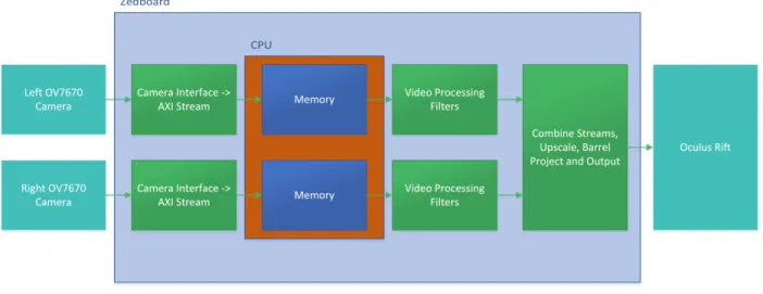
The system was designed to process video with as little latency as possible. For this reason, the team decided to try and put the majority of the modules in programmable logic (PL) rather than on the processing system (PS). This is because the PL is very efficient at doing parallel processing in real time. There is also a latency associated with moving video into and out of memory so it can be modified by the CPU, so these transactions needed to be minimized. When video comes from the camera, it must be either processed or buffered immediately as the camera will not stop capturing data. For this reason, the first goal of the system was to buffer the video in memory. This reduces the pressure on later video processing blocks since there is not a risk of losing parts of the frame. Next, video was processed to add the augmented reality component. It was decided to do the processing here so that it was running on the original resolution video from the camera, which reduces the processing power needed compared to processing the upscaled image. Last, the video had to be converted and output so that it could be viewed by the user.
The overall system design is divided into several functional blocks as seen in Figure 9. These include two hardware blocks, displayed in light blue, several blocks implemented in programmable logic on the Zynq chip, displayed in green, as well as a memory interface which uses the ARM processor on the Zynq chip, displayed in dark blue.
Figure 9: Overall System diagram
The first stage in the overall system is the input, which takes place in the OV7670 and Camera Interface to AXI Stream blocks. The first component is the OV7670 which is an inexpensive camera used to capture video input. This camera was chosen mainly for its price, and for the ease of interfacing with it. It is connected over a PMOD interface using a custom PCB to map the pins. It captures video at a resolution of 640x480. It is programmed, and data is captured through a camera interface block which is written in
VHDL. The block is responsible for programming the camera’s on board registers through an I2C interface and capturing video data from the camera. It captures the data 8 bits at a time and combines two groups of these 8 bits together into one 16 bit pixel. Last, the video signal is sent through a Xilinx IP block which converts it into an AXI stream. This allows stock Xilinx IP blocks to interface with the video. The input to the system is discussed in more detail in Section4.1.
During the next step in the pipeline, the video is saved to a frame buffer located in the DDR3 memory, which is external to the Zynq chip. This is done in order to allow the video processing modules to block if needed while processing data. Since the camera data is being stored they don’t have to worry about parts of the frame being lost if they don’t process it quickly enough. The memory buffer is triple buffered, which eliminates any tearing that may result from the frame changing while it is being read or written. On the Zynq chip, the memory access is controlled by the on board ARM Cortex A9 CPU, meaning that the programmable logic and CPU must work together in order to buffer video. On the programmable logic side, the module uses the Xilinx video direct memory access (VDMA) IP. In the CPU, bare metal C code interfaces with this block and controls memory access. More details about the buffering and VDMA is in Section4.3.
After being retrieved from the video buffer, the video is sent through various processing filters in order to augment the video with additional information. While in this proof of concept project, this module only highlights the difference between frames of video, other processes could be added here in the future that are specific to a certain application of the system. In this implementation, the video is passed through a delta filter, a thresholding filter, a median filter, and finally a Sobel filter. The delta filter, thresholding and median filter are written in Verilog, while the Sobel filter was written in HLS using the HLS video library. For more information on the video processing see Section4.4.
The last step of the system is to prepare the video for output and then output it to the DK2. Before the video can be output it has to be upscaled from the input resolution of 640x480 per eye to the output resolution of 1080x960 per eye. The video must then be barrel projected to correct for the pincushion distortion caused by the Oculus Rift lenses. Last, the streams from the two cameras, which have been processed separately, are combined. These processes are discussed further in Sections4.5and 4.6.
After the output processing, the video is ready to output to the DK2. The DK2, as discussed in Section
4.8, takes in video over HDMI, so the video must be converted from an AXI Stream to HDMI. In order to convert the video, the AXI Stream is passed into a Xilinx IP block called AXI Stream to Video Out. This block also takes video timings from a Xilinx video timing controller (VTC), which is programmed by the CPU. After the stream is converted to a video out signal, it is output to HDMI using an Analog Devices ADV7511 on the ZedBoard. This chip takes the video signal and converts to HDMI, before directly outputting to the HDMI port. The ADV7511 is programmed over an I2C interface controlled by the CPU.
4
System Implementation
This section will go into detail about how each part of design works. Each technology is described from a general standpoint, then how it was applied to the requirements of this project.
4.1
Camera and Camera Interface
The work done with the camera for this project consisted of three parts; altering the camera settings (registers), altering the camera capture logic, and translating the camera timing signals (href, vsync) to work with AXI Streams and Video Direct Memory Access (VDMA) (see Section4.3).
4.1.1 Camera Settings
The OV7670 has 202 registers that provide various settings for how the camera functions [20]. Even though the functions of some of these registers are documented, many are documented as ”reserved” but still impact how the camera performs. Undocumented registers were difficult to work with as the proper settings for this project had to be found through trial and error.
The main register settings that were modified were the video output format (COM7, COM13), to convert to YUV output, and data output range (COM15), to use the full scale output of 00 to FF. Most other register settings were either left as default value or changed to recommended values from online references (seeAppendix Dfor more details). Another key register is COM17, which provides an internal test pattern generator that can be used for testing color and timings. For a detailed list of all register settings see
Appendix D.
4.1.2 Camera Capture
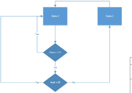
The initial camera capture logic was used from a similar project which built a system for outputting from the OV7670 camera module to a VGA display [21]. This interface was used to capture RGB data from the camera. The HDMI output for this project uses YUV, therefore the capture logic was redesigned to use YUV.
The camera logic uses a 2 state state-machine to keep track of what data is currently being sent. The first data packet sent after href goes high is dictated in the COM13 camera register, which is configured to send the U chroma value first. The data from then on will be in a known sequence of U (first value) ,Y,V,Y. However, because the video-in-to-AXI IP only expects a pixel package of either YU or YV, the camera capture logic does not need to keep track of whether it is outputting U or V. Figures10and11show this behavior.
State Function 0 • C = data
• WE = 0 1 • Y ¡= data
• WE = 1 Figure 10: State Machine for Camera Capture
Figure 11: Timing Diagram for Camera Capture
The state machine increments its state on every rising clock edge of PCLK. It resets to state 0 when vsync is high (new frame) or href is low (data for the row is not active yet). After which, on state 0, it assigns the data to an internal register C and sets the write enable to low, and on state 1 is assigns the data to an internal register of Y and sets the write enable to high. The output is then assigned to be C,Y according to the data expected from the video-to-AXI stream.
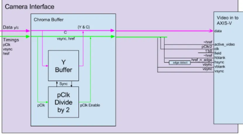
4.1.3 Camera Input Timings
The video IP used for DMA and Video Processing uses the AXIS-V format (see section4.2.4). The Video In to AXI4 Stream core is designed to convert standard computer video inputs such as DVI, HDMI, or VGA to the AXI format. Unfortunately, the camera does not conform to one of these computer video standards. The camera outputs only a few timing signals: Pclk, Vsync, and Href. The video core needs Pclk, Active Video, Hblank, Hsync, Vblank, and Vsync. Figure 12 shows how these timing signals work. In the case of syncing, there are options to use only the blank signals, only the sync signals, or all 4 signals for timing detection. Some adaptation between signals was needed in order to create the timing information for the Video In to AXI Stream core.
Figure 12: Video Timing Signals [22]
The adaptation used in the design alters and re-purposes the camera timing signals to conform to the inputs of the video in core. For Pclk, due to the methods used for camera capture, half of the camera’s pclk is used. This goes back to how the camera caputre logic only produces a pixel every other clock cycle. For Active Video, href is used. The href signal is active during the valid data of each row, so it is an acceptable replacement for Active Video. For hblank, the inverse of href is used. This signal is high whenever the data is not valid. To get hsync, an edge detector is placed on href. Hsync rises for a short pulse during the horizontal blanking period, after a row is finished. Only one high clock cycle of href is allowed to pass. For Vsync, the camera’s vsync is used. Vblank is not used by the video-in core and is simply passed through for
timing detection, which is not used in this project. The mapping of camera signals is shown inFigure 13. These connections are duplicated for both cameras in both sides of the pipeline
Figure 13: Video Input Block Diagram
4.2
Memory Interface and AXI Streams
In order to move data between different processes on both the programmable logic (PL) and pro-grammable system’s (PS) on the FPGA, various types of Advanced eXtensible Interface (AXI) buses are used. The AXI standard was developed by ARM under the Advanced Microcontroller Bus Architecture (AMBA) and contains several similarly-named but functionally different bus standards: AXI 3 and 4, AXI4-Lite, AXI4 Stream, and AXI4 Video Stream. These buses are integrally involved in most Xilinx Intellectual Property (IP) cores made for processing sequential data, including the Video Direct Memory Access core (VDMA) discussed in section4.3.
4.2.1 AXI 3, AXI 4, and DMA Transactions
AXI 3 and its generational successor AXI 4 are both standards intended for transaction based master-to-slave memory mapped operations. In this design, they are used for the transfer of data between the video pipeline in the Programmable Logic (PL) side and the main memory on the PS side. Some device controls also use AXI 3/4 as a trunk before being reformatted into individual AXI4-Lite interfaces. AXI 3 is hard wired in the PS since the PS is an ”off the shelf” ARM Cortex A9 processor and was not modified to upgrade to the newer AXI4 standard. Most interconnects on the PL side are done in AXI 4, with the exception of interconnects made to the PS.
Through AXI, a read or write to main memory is implemented as a periodic transaction originating from the PL side of the design. A Direct Memory Access (DMA) controller fabricates an AXI compliant
transaction and outputs it on the master bus. In the design, the DMA controller is a Xilinx IP core: the Video DMA (VDMA) controller. Data flows from the master bus to the PS memory controller. The PS memory controller is an arbiter for all the master buses on the PL and multiple other master interconnects for the ARM cores, caches, and snooper. When a transaction appears on any of these interfaces, it will be executed upon main memory.
In the case of writing to main memory, an AXI transaction contains the memory address to write to and a payload of configurable bit width/burst length. In the case of reading, the bus master (i.e. the DMA controller) provides an address and gives the slave device permission to use the bus to reply back with the data.
As might be implied, the AXI bus contains many signals and control flags. While there are timing diagrams for all the eccentricities of this bus, fortunately all of this has been abstracted away by Xilinx IP. All the interactions using a full AXI bus in the design are covered by Xilinx IP, and thus when considering using this bus one need only see to the proper configuration of IP and that the throughput and latency are sufficient. One need not worry about low level timings and interface operations.
4.2.2 AXI4-Lite
AXI4-Lite is a substandard of AXI4 that is intended for the configuration of memory mapped peripherals. Peripherals in this sense are any IP or hardware that is controlled by a processor such as a Microblaze or the PS system. AXI4-Lite lacks the extensive flags and timing conventions of full size AXI buses, using simpler logic that is feasible for frequent implementation in large designs with many peripherals. Thus it is not compatible with some of the more complex memory transactions (i.e. Bursts, Scatter-Gather) that full AXI buses are capable of. In this project, AXI-4 lite is used to configure Xilinx IP such as the Videe Timing Controller.
4.2.3 AXI4 Stream
AXI4 Stream (sometimes abbreviated AXIS) is significantly different from the previous two AXI buses in that it is not memory mapped. AXIS is a Master-to-Slave bus standard for controlling the flow of periodic data between modules, typically in a pipeline. It uses two flags: tReady and tValid to apply fore-pressure and back-pressure respectively, ensuring that modules connected together are operating at the same speed. In order to create an AXIS bus, only a clock, a data bus (tData), tReady, tValid, and reset are explicitly needed. Some additional control signals are optional, and most pipelines do not need them. Memory addresses are not needed in AXIS since the topology determines the source and destination of data. Due to this combination of design choices, it is fairly trivial to implement an AXIS interface for any logic that is designed to fit on a processing pipeline. In the design, AXIS is used in several niche cases such as for CORDIC rotations. Most
Figure 14: AXIS-V Ready/Valid Handshake [22] of the design is based on AXI Video Streams.
4.2.4 AXI Video Stream
AXI Video Stream (sometimes abbreviated AXIS Video or AXIS-V) is a standard for the payload of an AXI Stream and elaborates on the uses of two extra control signals: tUser and tLast. It specifies a large number of different standards for different video formats and resolutions, up to totally custom combinations. It also defines End of Line (i.e. hsync) and Start of Frame (i.e. vsync) using the tLast and tUser flags respectively. This standard is used throughout the project for the passing of video data between the various IP Cores, modules, and DMA controllers. In contrast to AXI4, it is significantly more import to understand this bus since it is much more feasible to write custom modules based on AXIS-V than full-fledged AXI4. Figure 14 shows the handshake between master and slave. Figure 15 shows some of the encoding this standard specifies, including the byte order for the most common formats.
Compared to the memory mapped standards, it is trivial to implement AXIS-V. In fact, in the design many of the custom designed HDL modules use the AXI4 Video stream bus format to communicate with each other and existing Xilinx IP.
4.2.5 Using AXI to design the system
A combination of AXI bus standards are used to create a complete video system. A diagram of clocking and data flow is shown in Figure16. There are three independently clocked pipelines in the system. The design is split into two overall halves, separated by DMA. The first half is associated with the clock and data flow of the cameras. Each of the cameras have their own free running clock and logic related to the cameras operate on these clocks. The logic is also operating under positive back pressure (i.e. pushing). The pixels
Figure 15: AXIS-V Format Codes and Data Representation [22]
streaming in from the camera cannot be stopped. Logic must always be ready to receive data. The second half of the design is tied to the HDMI clock, derived from the system clock. The logic is also operating under negative fore pressure (i.e. suction). The HDMI output cannot be stopped if pixels are not ready. Logic must almost always be ready to send data - there is a small FIFO that can absorb momentary halts. These timing constraints are the basis for needing VDMA.
Different types of AXI are used together on the design. In the first half of the design, data from the cameras is interpreted from its raw format and packaged into AXIS-V. During this conversion, the data is also re-clocked from its 24MHz clock to the internal stream clock of 148.MHz. The Video in to AXIS contains a FIFO for this purpose. While this does change the actual clock that the data is associated with, the amount, rate, and pressure constraints of the data stay the same. Many of the 148.5MHz clock cycles are not actively transferring data, and this builds in plenty of overhead for ensuring that data is always processed faster than the cameras output it. The AXIS stream is then passed into the DMA controller to be sent to a frame buffer in main memory over AXI4. The VDMA has a connection to main memory through the AXI interconnects, which are arbiters of all DMA traffic and convert between AXI4 and AXI3. In the second half of the design, data is pulled from the DMA controller as AXIS-V, processed to perform any augmented reality, stereo combined, and then output via HDMI. While examining this design it is important to note how all timing constraints converge on the DMA controller. Video is being forced into the frame buffer from the cameras, while being forcibly extracted from the frame buffer by the HDMI output. Each of these has its own clock where data needs to be taken in/output on every cycle, and all surrounding logic
Figure 16: Clock architecture on video pipeline. Video processing omitted
must be able to operate at this speed. The frame buffer created in main memory is able to pick up any error in the synchronization between each of the cameras and the HDMI output.
4.3
Video Direct Memory Access
Video Direct Memory Access (VDMA) is a crucial part of the video pipeline. It relieves the fore pressure and back pressure between the camera inputs and the HDMI output by creating frame buffers.
4.3.1 Frame buffers
All VDMAs used in the design implement a frame buffer in the DDR memory. The design requires two frame buffers, each of which should be at least capable of buffering an entire frame from each of the stereo pipelines. Considering that the cameras are using the YUV4:2:2 format, each pixel is represented by 2 bytes on average (chroma component sharing) and each frame is 640x480 progressive scan. Thus in order to buffer a single frame, 614.4KB of data must be stored. Considering 30 frames per second, this extends to a memory bandwidth of 17.58Mb/s. While these figures are not feasible to implement in BRAM, they are minuscule compared to capabilities of the external memory: 512MB of RAM, accessible from the PL at speeds up to 1.2Gb/s when reading at small burst sizes similar to those used in the design. Thus DMA is the ideal choice
Figure 17: Tearing [23]
for creating frame buffers in the project. While single buffers would be functional, the current DMA setup implements a triple buffer to avoid tearing and to allow frames to duplicate if necessary (i.e. 30fps in, 60fps out). This is closer to the default settings for the VDMA controller than single frame buffering.
In single buffering, the video input would trace along the frame buffer overwriting pixels as they are read in from the camera. The output would also trace along the frame buffer, although it may do so asynchronously to the input. This implies that at some point, the pointers of each trace could cross over each other. If this happens, an artifact called tearing will occur. In the middle of the output frame, a horizontal division will appear over which one frame appears and under which a different frame appears. The frame that appears under the tear depends on which trace is running faster: it could be an earlier or later frame relative to the image above the tear. This is very noticeable if the input is horizontally panning (i.e. the user turns their head side to side). SeeFigure 17for a demonstration of tearing when frames are horizontally panned images of each other.
is reading out video output pixel by pixel. When the video output has completed reading an entire frame and the video input has finished writing its frame, the two buffers switch roles so that the output reads the fresh input and the input begins overwriting the memory previously used by the output. This scheme will not work in this project because it requires the video input to be frame synchronous with the output. The video input must start writing to the frame buffer after the swap occurs and it must finish before the next swap occurs. This makes sense in video rendering applications where the video input can be controlled by vsync, but not in cases where the video input is a freely self-clocking camera. In this case specifically it will not work because the camera input must run at a slower speed than the output frame rate. If a synced input is not possible, tearing once again occurs, except it is written into the frame buffers as a result of the input trace changing buffers mid-frame as opposed to being an artifact of the reading trace in the single buffer example.
In a triple buffer, three frame buffers are used. At a given time, the input and output each operate on one buffer, while the third buffer contains an intermediate frame. By having three frame buffers, the input and output do not need to be synchronized for clean, tear free video. Suppose the output is running at a faster frame rate than the input as is the case in this project. When the input finishes copying in a frame, it switches to writing to the unused buffer. The freshly finished frame is scheduled to be the next frame the output will use. Meanwhile, the output is tracing through its frame buffer. When it gets to the end of the current frame, it may switch frame buffers. This depends on if a new frame is available from the video input yet. If no new frame is available, the same buffer is read again. A frame is duplicated. If a new frame is available, the frame buffer switches to the new frame and outputs this data instead. Suppose that the input was a faster frame rate than the output. The input will always switch buffers at the end of a frame, however the impact of this depends on if the output has begun reading the last frame or is still reading an older frame. The input cannot switch to the buffer that the output is using, so it may overwrite frames the output never read from. This isn’t an issue per se. The output will always begin reading a very recent frame from the input, however in extreme cases many input frames may be overwritten by the time the output gets to the end of its frame.
4.3.2 DMA Usage in Design
In order to implement a design meeting the video buffering requirements, the Xilinx AXI Video DMA controller is used. This controller supports an AXIS-V Input, an AXIS-V Output, and an AXI4 Master interface. It also has special I/O for communicating its status to other peripherals. What makes this controller unique from the other Xilinx DMA controllers is this controller fully implements the AXIS-Video standard and is aware of frame buffers, as opposed to plain FIFOs or fully manual DMA transactions implemented by other designs. It maintains its own internal pointers to memory that automatically move
between one or more buffered frames as video input and video output send/request data. Again, it is frame aware, not just a FIFO, and it knows how to do multiple frame buffering. To enable this functionality, some configuration is required in hardware and significant configuration is required at run time which is setup in software and sent over AXI4-Lite. These processes are described further in Section4.3.3.
Two VDMAs are used in the Design, with one VDMA for each camera. The VDMAs are used to create a frame buffer so that differences in the running speed and frame position of the camera and HDMI output can be handled. The VDMA is placed immediately after the Video In to AXI Stream Core and stores YCbCr 4:2:2 640x480p video into a triple buffer. The genlock mode is set to dynamic master/dynamic slave, so that the write half of the VDMA controls two frame buffers and tells the read half of the VDMA which frame buffer to read from. At run-time, software configures the VDMA for operation. The Frame buffer locations are set for each VDMA in main memory, the resolution is configured, and the VDMA is set to run as soon as video input appears.
4.3.3 Hardware configuration of VDMA
The hardware configurations for VDMA are not as intuitive as they may seem but once understood can be leveraged to perform many useful DMA operations. These settings are entered through the IP customization interface in the Vivado development environment. Most of them have an effect on which operations can be performed with the unit after it is synthesized since disabling certain functions will remove the requisite logic from the DMA unit’s HDL. The VDMA module must also be properly connected to the video pipeline and to the PS in order to access main memory.
One of the first settings is enabling or disabling the read or write channels. By default, the VDMA unit has both a read and write channel, which makes sense in the context of a frame buffer. Data copied into main memory is read back on demand. In applications where video is rendered by the CPU into a location in main memory, VDMA may be used with only a read channel to copy data out. Alternatively, in an application where the CPU performs some terminal video processing, VDMA may be used with only a write channel to copy video into a location in memory. In the project a frame buffer was needed so all VDMA units have both channels. There is also an option inside the IP configuration panel to select the number of frame buffers, which was set to three for this project. This is cosmetic and merely initializes a register. Almost all implementations of run time software will overwrite this register with a value stored in the configuration program, but there is no harm in having the intended value entered here.
Within each of these channels there are options to set burst size, stream data width, and line buffer depth. There are FIFO buffers built into the VDMA unit since the VDMA unit needs to packetize its transactions with main memory. The VDMA unit must accumulate at least one packet’s worth of data in order to start a write transaction. In order to guarantee that video is available to subsequent modules on
the pipeline at all times, video must be prefetched several hundred pixels in advance to hide the latency of accessing main memory. The channel settings affect how much data each transaction will contain and how aggressive the VDMA will be about pre-fetching video from main memory. Larger burst sizes and bus widths are more efficient and must be used for a high performance video system (i.e. 4K video) since the overhead associated with transactions can quickly add up. Larger FIFO sizes are also needed on high performance video pipelines since the latency of communicating with main memory can quickly exceed the time in which the FIFO can be emptied by video processes down-pipe. For this project, default settings were used since the video processing does not come near the performance limits of the Zynq system. A burst size of 16 pixels with a 16 bit bus width and a line buffer depth of 4096 were used.
Fsync has different purposes on the read and write channels. On the write channel, fsync is extremely important and not set by default. An fsync signal indicates the separation between frames of video. The VDMA needs an fsync source in order to separate frames of incoming video into their proper frame buffers. Without this, frames will start at an arbitrary point in the frame and will not be properly aligned within the frame buffers. An arbitrary start of frame will be selected based on the assumption that the first data the VDMA receives is from the first row and pixel. In most applications, the s2mm tUser option is the correct setting. This will use the AXIS-V format’s built in Start-Of-Frame signal to determine the vertical sync position. On the read channel, fsync serves a completely different purpose. Often, a device outside of the FPGA will be clocking frames. For example, a device combining two DVI or HDMI inputs that does not have its own frame buffers will use an external fsync to synchronize its inputs. The VDMA has a line for an external fsync so that the video coming out of the video pipeline will be synchronized with the external device.
Genlock is a very pivotal setting that affects how the VDMA will sequence through frames. Dynamic master and dynamic slave are used together if it is desired for the VDMA to internally perform a triple buffer operation such as the one described in Section4.3.1. Dynamic refers to the fact that the read and write channels of the same VDMA unit will use an internal bus to communicate with each other about what to do. Read and write may take either role (master or slave), depending on preference. Master will own all but one of the frame buffers, and slave will be told which remaining frame buffer to use. Dynamic-Master/Dynamic-Slave for write/read respectively is the selection used in this project. Master can be used in a situation where only a read or a write channel is being used, or two separate VDMAs units are being used each with one channel. In slave mode, VDMA will be programmed with a list of possible frame buffer memory addresses and will select a buffer as indexed by a hardware interface. Slave/slave is a mode that was attempted in this project when the CPU was performing video processing and needed explicit control over the frame buffer usage. Unfortunately, this method was unsuccessful and removed when all the video processing was redesigned to work in the programmable logic.
Unaligned transfer is an advanced setting which enables the generation of some additional hardware that utilizes the advanced functions of the AXI3/4 bus to perform memory transaction that are not aligned with 16, 32, or 64 byte lines of memory. Accessing memory starting at bytes aligned to a certain minimum power of two is optimized on almost all computer architectures. Most applications don’t need to use specific bytes and a wisely chosen address for the frame buffers and burst size will sidestep this problem. The unaligned transfer function was not used in the project.
The VDMA unit must also be be connected to the PS system. In Vivado, the PS is represented as an additional IP module ”Zynq7 Processing System”. This module almost has to be used in the block design layout tool in the Vivado development environment, which automates wiring up complicated buses and packaged IP heavy projects. Xilinx Product Guide 082 has more information on this module. In short, the Zynq IP module is the interface used to tell the implementation tool chain to connect nets to features of the PS system, and it also includes many settings that will affect PL and external facing resources of the PS system (i.e. clocks, interrupts, specialty buses). The VDMA’s AXI4 Master interfaces need to be connected to the High Performance (HP) AXI3 slave ports on the PS system. Due to the difference in protocol version, an AXI memory interconnect is needed between these devices. An AXI4-Lite bus needs to be connected from the VDMA units to the AXI3 GP Master ports on the Zynq7 module. Again, due to protocol version differences this needs to pass through an AXI memory interconnect. The clock and resets nets need to be setup and routed for these AXI3/4/Lite buses. An 148.5MHz clock derived from the PS’s fclk is used for all buses (stream interfaces included). Use of one clock helps synthesis by simplifying timing constraints. These fclk clocks have special resets, and a ”processor system reset” IP core is needed to format and distribute two separate resets to all IP on these AXI3/4 buses. One reset is used to reset interconnects, and a separate reset is used to reset the peripherals connected to these interconnects. Most of the wires and IP up to this point are all automatically created and routed with the Vivado Designer Assistance’s connection automation tool. Once these connections and hardware are created, the actual video stream (i.e. AXIS-V) inputs and outputs need to be wired up. This is application specific. For testing only, a test pattern generator is wired into the input, and the output is connected to a working HDMI output stage. For design implementation, the input is connected to the cameras, and the output is connected to the first module in the video processing pipeline.
4.3.4 Software configuration of VDMA
Most of the VDMAs settings are configured at run time by software running on a processor. In simpler projects, a Microblaze soft core processor can be used to perform this configuration. In this project, the ARM cores on the Zynq perform these operations. The source of the code used for software configuration was adapted from an Avnet example project, and due to the license agreements and publishing restrictions on
this code it is not included with this report. This code can be found on the Avnet website under design name ”FMC-IMAGEON HDMI Video Frame Buffer”. The settings configured are important but generally easy to understand, and they can be leveraged to achieve some fairly complicated operations with the VDMA IP. The following settings are configured in software, some of which may overwrite options set in IP configuration tool in Vivado.
• Input, Output, and storage frame size/resolution
• Stride setting (the size of a pixel in bytes)
• Parking settings (stopping after a certain number of frames)
• Genlock mode and source for each channel
• Number of frame buffers
• The base address in main memory of each of the frame buffers (independent for each channel)
• Start/stop of VDMA
• Checking of error flags and dumping of registers for configuration verification
All of the functions used for this configuration are generated by the Xilinx SDK through a board support package (BSP). BSPs will generate an API of functions and constants for hardware modules that are included in a hardware description file (HDF). A HDF is automatically exported from Vivado when creating an SDK environment associated with a hardware project. The HDF contains information about what Xilinx IPs have been created in a project, how they are connected to the processors, what the base address of their registers are, and what their IP customizations are. This process can be extremely finicky if any of these files/packages are not updated when hardware changes.
4.4
Image Processing
The image processing steps implemented in this project are based on a previously implemented object tracking algorithm [24]. These processes are meant as a proof of concept for an advanced image processing technique that could be implemented in this sort of project. This section provides an in depth look at the techniques and implementation of the video processing steps involved for this project.
4.4.1 Grayscale
All the video processing done in this project uses grayscale images. This is important because in grayscale, objects in an image are more pronounced from each other and easier to separate. Also, many video filters are not applicable to a color image. Luckily, in the image format this project uses, YCrCb, the Y component of the image represents the grayscale image. Therefore, to convert to grayscale, the Y component can be processed separately, whereas in RGB, additional calculations have to be done on the image in order to
get the equivalent grayscale image. This reduces the calculations the system needs to perform and also eliminates one source of potential error.
4.4.2 Delta Frame
The delta frame filter finds the absolute differences between two frames. For every pixel i in the output frame, the value is the absolute difference of the value of pixel i in frame 1 and pixel i in frame 2.
OutputF rame[i] =|F rame1[i]−F rame2[i]| (1)
These differences highlight the parts of the image which have changed between the two frames. Figure 18
shows this process in detail. Frame 1 and 2 represent the two frames being processed. The object in frame 2 is slightly shifted right from that shown in frame 1. The combined frame would be the resulting frame if they were simply combined. The resulting figure shows the result of the delta frame calculations. It is important to note that the black figure would not turn white, but it would be separated from the black background as shown.
Figure 18: Delta Frame Process
This process is useful for eliminating background from moving objects in a video. Figure 19 shows this process being performed on real video of a hand moving through the frame. In the before picture, there is a lot of background in the image (laptop, wall, etc). However, because they are not changing from frame to frame, they are removed in the delta frame process because they are subtracted from themself, and what is left is only the moving hand (more can be seen athttps://youtu.be/2wbC4cexFb0).
This processing is most useful when performed on two consecutive frames. By doing this, the output will highlight the objects in the frames which have moved between the two frames. This is highly dependent on
Figure 19: Delta Frame Calculations on a Video of a Moving Hand
the frame rate at which the video being processed. At low frame rates, there could be large changes between two frames, which would result in a convoluted output frame. However, at high frame rate, smaller changes can be detected, which means a more meaningful result on fast moving objects.
4.4.3 Thresholding
Thresholding is the process of setting all values below a cutoff value to 0. This reduces the amount of noise in the image that can be caused by small differences in the frames before the delta frame calculations. These differences can be caused by lighting or resolution. If the cutoff value for the threshold is too low, some of the noise that should be getting removed stays and can change the processing later on in the pipeline. If the cutoff value is too high, some of the values that are relevant to data processing can be removed, and therefore the desired video might not output. This means choosing a threshold value is an important step. There are processes for dynamically choosing the threshold (detailed in [24]), however, these add additional logic and unreliability to the system for a small improvement in desired output. In addition to removing all values below a threshold, is order to assist in processing later on in the pipeline, all values which are not removed are set to the max value, 255.
4.4.4 Median Filter
A median filter is another way to remove noise from an image. Median filter works by assigning each pixel to the median value of all its adjacent pixels. This processing is similar to averaging the pixels of the image, however is less sensitive to large differences in values. This is important because previous to this step, thresholding was performed on the image. This means there will only be values of the lowest value or the max value, so there will be many of values of 0 and 255, but none in between (for more information see Section4.4.9).
Figure 21: Sobel Masks[25]
Figure 20shows the results of the median filter applied to the result of delta frame and thesholding. As can be seen in the figure, the image on the left has more noise that was not caught by the thresholding, that should be removed before processing is continued. The median filter also can remove negative noise as can be seen in the white object in the image. The median filter inserted white into the object, where noise caused the delta frame to remove data.
4.4.5 Sobel Edge Detection
Sobel Edge Detection is an algorithm for highlighting edges in an image. It works by applying a mask to each pixel in the image (shown inFigure 21). That pixel is then assigned the magnitude of the result of the mask (as shown inEquation 2). Most systems simplify this equations by using an approximation shown inEquation 3.
|G|=qG2
x+G2y (2)
|G| ≈ |Gx|+|Gy| (3)
The result of the Sobel Edge Detection Algorithm is an image where all of the edges of objects have a high value (close to white), and everything else has a low values (close to black). The result can then be run through a threshold to reduce leftover noise in the image. A result of the Sobel edge detection can be seen inFigure 22. When run on the result of the delta frame, the highlighted object which has moved will be clearly outlined in the image.
4.4.6 Implementation
The implementation of the delta frame and thresholding can easily be done in hardware. Using AXIS-V, the delta frame implementation is relatively straight forward. The same holds for the thresholding as well. Xilinx also provides implementations of these two functions. However, because they are based on the OpenCV library, they are overly complex for the purposes the application of this project.
![Figure 2: Marketing design for Continental Heads-up Display[11]](https://thumb-us.123doks.com/thumbv2/123dok_us/10968064.2985006/15.918.285.633.107.360/figure-marketing-design-for-continental-heads-up-display.webp)


![Figure 12: Video Timing Signals [22]](https://thumb-us.123doks.com/thumbv2/123dok_us/10968064.2985006/25.918.251.672.384.761/figure-video-timing-signals.webp)
![Figure 14: AXIS-V Ready/Valid Handshake [22]](https://thumb-us.123doks.com/thumbv2/123dok_us/10968064.2985006/28.918.133.794.118.357/figure-axis-v-ready-valid-handshake.webp)
![Figure 15: AXIS-V Format Codes and Data Representation [22]](https://thumb-us.123doks.com/thumbv2/123dok_us/10968064.2985006/29.918.182.741.106.460/figure-axis-v-format-codes-data-representation.webp)
