Detecting E and H Fields with Microstrip
Transmission Lines
Tze Wee Chen Centre for Integrated Systems, Stanford University, CA 94305,
USA
Timothy J. Maloney
Intel Corp., 2200 Mission College Blvd., Santa Clara, CA 95054, USA
Bruce Chou
Intel Corp., 2200 Mission College Blvd., Santa Clara, CA 95054, USA
Abstract- Microstrip-like transmission lines are used to detect transient electric and magnetic (E and H) fields. Theory and experiment are compared for three different cases. The method can detect E and H fields on a ground plane, or may be
integrated into a closed platform for E-H measurements during
EMC testing. An application example using a desktop computer is shown. In situ measurements in a closed platform during EMC
testing show that system ESD failures are caused by E-H fields,
and not by direct voltage or current stress. Therefore, E-H field
information measured by using microstrip-like transmission lines on PCBs in a closed platform during EMC tests will give insights to the exact nature of system failures due to ESD.
Keywords- ElectroMagnetic Compatibility (EMC), Printed Circuit Board (PCB) detectors, Charged tip discharge.
I. INTRODUCTION
Due to the proliferation of electronic products, commercial electronic products need to pass stringent tests for ElectroMagnetic Compatibility (EMC) to ensure reliable operation in the field. One way to test for EMC is to use a gun in accordance with IEC 61000-4-2 and try to induce soft system failures. While this test system is well-specified and well-modeled on the circuit level, the fields it generates are not as well-studied [1]. This causes difficulty in interpreting the test results. In particular, there is a large range of test voltages at which soft system failures may be induced, depending on the location at which the test gun contacts the chassis. Ensuring that the product does not fail for the lowest test voltage at which soft system failures are induced regardless of where the stress is applied is clearly overly pessimistic. There are also cost-related considerations for such an over-design protection strategy. A more thorough understanding of why and how soft system failures are induced during ESD stress, and a new metric for determining stress thresholds is highly desirable.
To get more relevant data about why and how electronic systems fail in the presence of discharge events, more information is needed about the electric and magnetic fields inside the box when the failures occur. While antennas can be put inside the boxes to measure the fields easily, routing the detected signals out of the boxes require more thought. Introducing artificial apertures, or worse, using an open box, in order to route the detected signals out of the box will cause the measured signals to be unrepresentative of field conditions.
In this work, we present a novel method to detect electric and magnetic fields inside an electronic product using a PCB
trace line or equivalent transmission line detector so that the detected signals are representative of the fields induced during both the EMC test and field conditions. The field detection method is described, followed by three examples of the method, with theoretical analysis and experimental results. Finally, some application examples are given. In one, a field detector is implemented inside the casing of a personal computer, and it is shown that there is a threshold field strength beyond which the system fails predictably. In another, we implement a novel 50-ohm line inside the box.
II.FIELD DETECTION METHOD
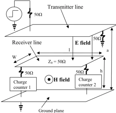
This work proposes a novel detection method for transient electric (E) and magnetic (H) fields by using a transmission line as a receiver. As an example, consider the case when there are vertical electric fields and horizontal magnetic fields, with the latter normal to the cross-sectional loop area of the receiver line, perpendicular to the line length (Fig. 1).
A. Charge induced by Electric field
From Gauss’ Law, the charge Qsum on top of the line with field E (volts/meter) is, neglecting fringe field effects,
0
(1)
sum
Q
= × × ×
ε
E l W
In the case of a transient electric field step, that amount of charge is associated with the E field step size. Thus the field has changed by ∆E due to charge flowing off both ports, so
0
(2)
sum
Q
E
l W
ε
∆ =
⋅ ⋅
Clearly the measured signal indicates time derivative of the field as long as the line is electrically “small” compared to the spatial extent and wavelength of the fields. This means that, for this electrically “small” line,
0
(3)
sumi
dE
dt
=
ε
⋅ ⋅
l W
B. Charge induced by Magnetic field
For detecting magnetic fields, consider the magnetic flux step on the receiver line with characteristic impedance Z0. The flux can be expressed as
(4)
LI
or using Faraday’s Law, for H normal to the line area as in Fig. 1,
0 0 0
2
2
(5)
diffV
t
I Z
t
Q
Z
H l h
µ
× ∆ =
×
× ∆
=
×
=
× × ×
This time, the charge packet Qdiff is measured as the difference of the two channels because of the nature of Faraday’s Law and Lenz’s Law, as the effect is to induce a current in a particular direction (opposing the H field flux) and to do so without inducing a net amount of charge. Thus a differential charge packet Qdiff measured over time ∆t indicates a magnetic field change ∆H in amps/meter. The change in field strength can be found as
0 0
(6)
diff
Q
Z
H
l h
µ
⋅
∆ =
⋅ ⋅
So for an electrically small line as above,
0 0
(7)
diff
i
Z
dH
dt
µ
l W
⋅
=
⋅ ⋅
C. Measuring Qsum and Qdiff
It follows that Qsumand Qdiff can be physically measured by placing two charge counters, one at each end of the receiver line.
In this work, another 50 Ω transmission line acts as the transmitter. A voltage step is sent onto the transmitter line in order to set up the transient E and H fields, which is to be detected by the receiver line. As shown in Fig. 1, the transmitter line is distance a above the ground plane. Clearly, the E and H fields set up in such a manner will depend on the nature of the dielectrics in between the receiver line and ground plane, and transmitter line and ground plane. In Sections IV to VI, different combinations of dielectrics are experimentally measured and compared with analytical calculations. Through these experiments, it will be shown that the formulations presented in this section are valid for detecting E-H fields set up by EMC tests, and enables in situ
measurements of E-H fields in a closed platform.
Figure 1: Transient electric (E) and magnetic (H) fields as described in the example. Two transmission lines with characteristic impedance of 50Ω are used, one as the receiver and the other as a transmitter.
III.AIR LINE DETECTOR
A. Setup
The simplest case is when there is only air as a dielectric for both transmitter and receiver lines. A receiver line was fabricated as a microstrip, with its width (W=2.5 cm) and height (h) above the ground plane calculated so that the resulting impedance of the receiver line is 50Ω. This arrangement would be suitable for fields on an IEC gun target ground plane [2]. A voltage pulse was sent onto the receiver
line as part of a matched 50Ω delivery system.
Experimentally, there is almost zero reflection, so the receiver line is very close to being 50Ω as expected.
The transmitter line was made in a similar manner, W=10.5 cm, and positioned on top of the receiver. In this way, the receiver sees a uniform electric field when a voltage step is applied on the transmitter.
One end of the transmitter line is connected to a pulse generator, and the other end is terminated with 50 Ω. As such, a pulse may be sent onto the transmitter line without reflections because of the impedance match. This pulse will set up transient electric and magnetic fields, which can be detected by the receiver line. Both ends of the receiver line go to oscilloscope channels, which act as charge counters on both ends of the receiver line.
B. Results
The electric field under the transmitter line is simply
(8)
V
a
E field
h
Charge counter 1
Charge counter 2 W
l
Receiver line
H field
Ground plane Z0 = 50Ω
50Ω 50Ω
Transmitter line
a 50Ω
where V is the voltage on the transmitter and a is the distance from the transmitter line to the ground plane, as shown in Fig. 1. For this parallel plane TEM mode in free space,
377 (9)
E
H
=
Ω
The total charge caused by the electric field, E, expected to be collected by the receiver when an input step is sent onto the transmitter is then
(
0)
( )
(10)
sumQ E
C V
E
l W
Q
ε
= ⋅
= ⋅
⋅ ⋅
=
Analogously, the differential charge caused by the magnetic field, H, when it is normal to the receiver loop is
(
0)
0
( )
(11)
diff
l h
Q H
H
Z
Q
µ
⋅ ⋅
=
⋅
=
where Z0 is 50 Ω.
The actual charge collected by the receiver line due to a step on the transmitter line can be measured physically. This charge is
0
(12)
Q I t
V
t
Z
= ⋅
=
⋅
For charge induced by the electric field (Q(E)), V is the sum of the voltages at both ends of the receiver as described earlier. For charge induced by the magnetic field (Q(H)), V is the difference of the voltages on both ends of the receiver. We confirmed that the desired sum and difference signals can be produced with 0 and 180 degree splitter/combiner modules, as one would often want to employ in E-H field measurements. In these studies of step response, usually we looked at each receiver channel on the oscilloscope and integrated the pulse resulting from the step. Figure 2 shows a typical oscilloscope measurement. Qsumis the sum of the areas under Channels 2 and 3, and Qdiff is the difference of the areas under Channels 2 and 3.
Both expected and measured charge induced by the electric field (Eq. 10) and the magnetic field (Eq. 11) are plotted for a series of voltage pulses sent onto the transmitter line. The measured charge agrees with the calculated charge for this detection method to within 13% for both the E and H fields.
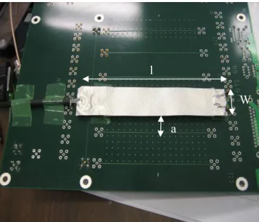
IV.PCBLINE
A. Setup
A realistic case for platform EMC will be for the receiver line to be a trace on a Printed Circuit Board (PCB). In the test case, a 50Ω transmitter is built above the receiver similar to the air line configuration (Fig. 3). The receiver is now built on the PCB and can be used to sense the E and H fields inside a
closed box. Such a setup would be useful for platform EMC in situ measurements.
Figure 2: Typical oscilloscope reading used to calculate Qsum and Qdiff. Qsum =
Ch2 Area + Ch3 Area, Qdiff = Ch2 Area - Ch3 Area. Ch 1 is the voltage step,
measured upstream of the Transmitter line (Fig. 1), which has a slight mismatch to 50 ohms.
l
W
a
Figure 3: Air line above PCB trace line as the receiver.
B. Results
The analysis of this setup is complicated by the dielectric layer of thickness h between the receiver trace line and the board ground. The effect of this additional dielectric layer cannot be ignored.
An independent pulse measurement of the PCB shows that the trace impedance, Ztrace, is 55 Ω. Also, the velocity on the trace line, v, is 1.92x10⁸ ms-1.
1
(13)
tracetrace
C
v Z
=
⋅
The voltage on a PCB receiver line of finite metal thickness
t and separated by h from ground is difficult to know but can be estimated from the air line pulse voltage V as
1
(14)
trace
r
V
t
V
h
a
ε
h
⎛
⎞
= ⋅ ⋅
⎜
+
⎟
⎝
⎠
where εr is the relative dielectric permittivity of the board
dielectric.
The total charge caused by the electric field, E, expected to be collected by the receiver when an input step is sent onto the transmitter is then
( )
(15)
trace tracesum
Q E
C
V
l
Q
=
⋅
⋅
=
where l is the receiver line length.
Analogously, the differential charge caused by the magnetic field, H, expected to be collected by the receiver is
(
0)
0
( )
(16)
diff
l h
Q H
H
Z
Q
µ
⋅ ⋅
=
⋅
=
where Z0 is 50 Ω.The actual charge induced by the E and H fields can be measured using a similar procedure as outlined earlier. The calculated and measured charge induced by the E and H fields caused by sending a step onto the transmitter line agree to within 20% for this detection method after accounting for second order effects such as trace thickness and fringing fields. Another variation of this same setup is to have the receiver line perpendicular to the transmitter line. In this situation, charge will only be induced by the electric field and not the magnetic field.The calculated and measured E fields agree to within 6% for this case; measurements show that the H field was indeed negligible, as expected.
V.POST TRANSMITTER
A. Setup
The final case analyzed in this work is when the transmitter is a vertical post. This situation is similar to a charged tip and shaft, such as that of a screwdriver, approaching a ground plane.
The 50 Ω receiver line used in the air line configuration is used here. In this configuration, a shorted semi-rigid coaxial cable is used as the transmitter, equivalent to a solid metal post (L-C post in Fig. 4). The post is connected to a high voltage supply, and approaches the ground plane until it touches the ground plane. As the charged post approaches the ground plane, electric field builds up between the tip of the
post and ground until air breaks down and a spark discharge occurs. This discharge causes transient E and H fields which
an be picked up by the receiver line.
B. Results
dewall capacitance of a post approaching a ground plane by
c
From earlier work on the inductance of a post [3], it is reasonable to approximate the si
0
2
(17) ln( ) 0.73
x C
x a
πε =
tion, where the additive constant b n2 or abo t 0.693.
r line is distance d away from where the L-C post contacts the ground ane.
or line at radius x, corresponding to height x on the post, is
+
where a is the radius of the post, as shown in Fig. 4. A similar view of sidewall capacitance, and accompanying inductance, appears in a classic treatment [4] of the monopole antenna as approximated at each height by a biconical antenna. This latter treatment focusses on the small angle approxima
u ecomes l
Figure 4: L-C post as a transmitter, with its electric field before discharge. The receive
+V
E
x 2a
L-C
post
d
Receiver
line
pl
With the expression (17) for capacitance valid for x/a
greater than about 4 [3], the differential charge density on the detect
0 2
ln
0.73 1
(18)
ln
0.73
x
V
a
x
x
a
⎢
⎝
⎝ ⎠
⎠
⎥
⎣
⎦
Therefore, the total
σ ε
⎡
⎛ ⎞
⎤
⎢
⎜ ⎟
+
−
⎥
⎝ ⎠
⎢
⎥
= ⋅ ⋅ ⎢
⎛
⎛ ⎞
⎞
⎥
⎢
⎜
⎜ ⎟
+
⎟
⎥
charge induced on the receiver line by the electric field step,
x
where x1 and x2 are the bounds of the receiver. .
∫
=
1
(
)
)
(
x
x
dx
W
E
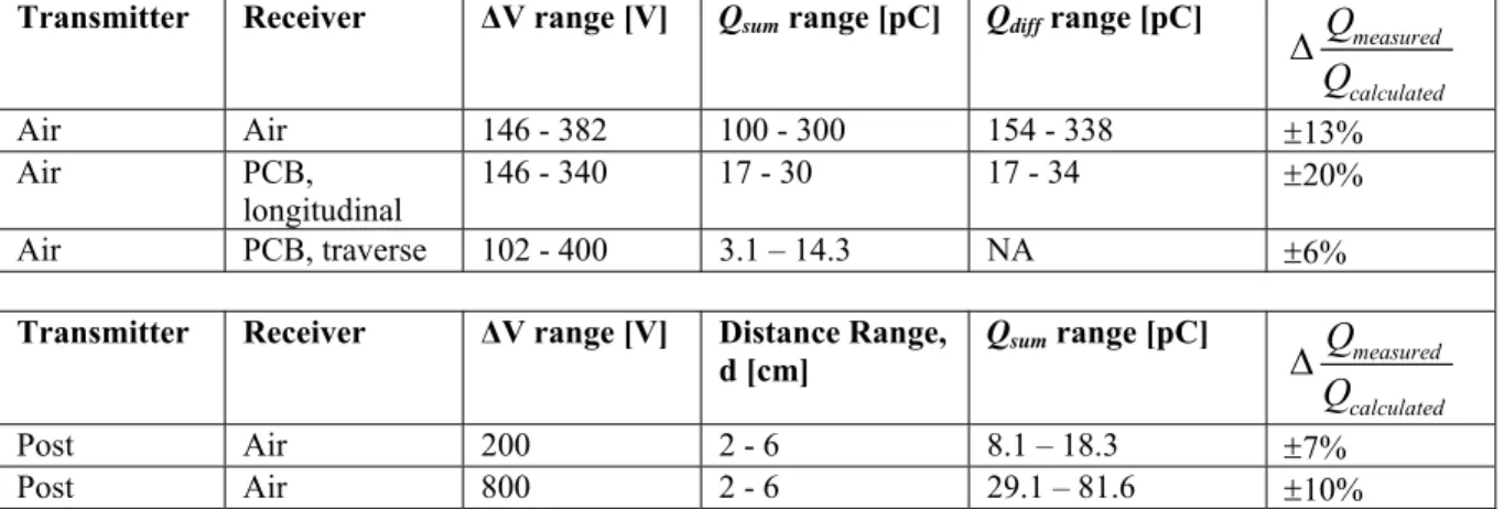
Table I: Table summarizing the measured and calculated charge induced by E-H fields for each of the three setups described in Sections IV to VI.
Transmitter Receiver ∆V range [V] Qsum range [pC] Qdiffrange [pC] measured
calculated
Q
Q
∆
Air Air 146 - 382 100 - 300 154 - 338 ±13%
Air PCB, longitudinal
146 - 340 17 - 30 17 - 34 ±20%
Air PCB, traverse 102 - 400 3.1 – 14.3 NA ±6%
Transmitter eceiver R ∆V range [V] Distance Range, range [pC]
d [cm] Qsum measured
calculated
Q
Q
∆
Post Air 200 2 - 6 8.1 – 18.3 ±7%
Post Air 800 2 - 6 29.1 – 81.6 ±10%
Using the relationships
(
0)
( )
(20)
Q E
E
l W
ε
=
⋅ ⋅
and(
0)
0( )
(21)
Q H Z
H
l h
µ
⋅
=
⋅ ⋅
E and H fields can be measured as before. In this case, the charge from the collapsing E field is similar to the setups described above. However, the current causing the H field comes from the discharge of a log-tapered transmission line, as it were, and the exact waveform has not yet been calculated. The E field is a step, but the current and H field start and stop at 0 over the course of that step.
The total charge induced on the receiver line depends on the location at which the post contacts the ground plane. Charge induced by the E field is measured as a function of the distance, d (Fig. 4), between one end of the receiver line and where the post contacts the ground plane. Calculated charge using Equation 19 agrees with the measurements to within 7% when the high voltage is set to 200 V, and 10% when the high voltage is set to 800 V. In both instances, the experimental data match the theoretical calculations well for E field.
Table I summarizes measured and calculated charge induced by E-H fields for the three different setups described in sections IV to VI.
VI.SYSTEM ESDEVENTS
detector thus indicated the general level of fields (and their
co
will fail. This supports our notion that, for
the In this section, an application example for a desktop personal computer system ESD test is described. A field detector was implemented inside the chassis behind a BNC connector, in this case an H field detector made up of a 6 cm shorted loop of 24 AWG wire. The separation between the wires is 1.5 cm, which means that the impedance of this loop is about 489 Ω (note that we now tend to fashion all loops as shorted transmission lines that will double the H-field signal and cancel the E-field signal). In order to induce soft failures on a powered-up system, we had to feed the IEC gun pulse into the chassis with an insulated wire, routed past a motherboard section and grounded to the chassis. The H field
time derivatives) injected into the chassis and put out several volts peak-to-peak (Vpp) into 50 Ω. Since the insulated wire
was not directly connected to anything but the chassis, the system failure is thus caused by the transient internal electric and magnetic fields, which were found in this arrangement to scale directly with the test voltage. In other words, there is no direct voltage or current stress to any of the components on the motherboard; the only disturbance caused by the IEC test gun is to the E-H fields inside the chassis.
A test gun whose output waveform conforms to IEC 61000-4-2 was used to stress the platform. Twenty
nsecutive voltage pulses were sent onto the wire for each of five test voltages, and Vpp for the field detector was recorded
from the oscilloscope. The total number of system failures caused was noted, and test results appear in Fig. 5. Note that Vpp is not the IEC gun test voltage, as is typical for these tests.
Instead, Vpp is the voltage induced by the stress voltage on the H field detector.
Fig. 5 reveals a fairly sharp threshold field strength beyond which the system
an ordinary IEC gun test on the external chassis, the amount of field leaking into the system is a better measure of system stress than the test voltage by itself. Since soft system failures are not caused by direct voltage or current stress on the system components, specifying a threshold field strength that will not cause the most vulnerable component to fail is the most efficient protection strategy.
It is worthwhile to note here that it is current industrial practice to measure system ESD robustness as a function of IEC test gun voltages that cause failures. Since the E-H
fields that leak into the chassis depends on many factors, including the relative positions of any apertures and the point at which the IEC test gun contacts with the chassis, it is clear that the IEC test gun voltages that cause soft system failures do not provide sufficient information about the exact nature of system failures by themselves. In contrast, in situ
2 3 4 5 0
20 40 60 80 100 120
V
pp [V]
F
a
ili
ng P
e
rcentage [%
]
Failing Percentage
Figure 5: Failing percentages for the system under test for different test voltages (shown as field measurement; 4.86 Vpp corresponds to 1.2 kV on the IEC gun). 20 consecutive tests were performed for each test voltage level.
As we go to press, we find more evidence that microstrip field detectors, embedded inside a system, are very useful for learning about fields injected during an IEC test. Our first true transmission line detector was installed inside a desktop PC platform, with a flat aluminum panel serving as the ground plane. The 50-ohm transmission line formed atop this ground plane was about 10 cm long and was made from plastic-enclosed “twin lead”, ordinarily a 300-ohm parallel-wire transmission line about 7 mm across. The wires were shorted together at the SMA connector posts at each end. With some quick calculations of the two parallel wires and their images in the ground plane (hint: you need to use the acosh expression), we had realized that such an assembly should work out to be a 50 ohm line. Remarkably, it was confirmed to be 48-52 ohms with z-match experiments.
The twin lead 50-ohm had a loop height, wire width, etc. that predicted a signal strength about 10-15X higher (in voltage and current) than the same length of 50 ohm line on the PCB, now opposite the detector. Therefore we were able to acquire a strong signal, believed to be a scaled version of what the board components picked up due to the fields. The first few results were quite intriguing—we seemed to have a platform box resonance that was close to an I/O clock frequency, but it was not always excited by the external IEC zap. But when the resonance was excited, the platform was sensitive to lockup.
VII.CONCLUSION
This work describes a novel method that can be used to detect E and H fields caused by system ESD events [5]. Theoretical analyses of three different cases have been shown to match experimental data well. With this method, microstrip transmission lines can be designed on ground planes to detect
E and H fields, or on PCBs to detect E and H fields inside a system during system ESD testing. We see, for example, the H-field loop detector on a ground plane to be similar to our line detector but with a shorting termination instead of a z-match. Instead of being concerned with undesired E-field effects and the (round trip) time lag of E-field cancellation on
such a detector, we see the benefit of extracting both E and H field information from a single z-matched line detector where time lag effects are cut in half.
An application example of this detection method was implemented for a desktop computer system ESD test. In situ
measurements in a closed platform during EMC testing show that system ESD failures are caused by E-H fields, and not direct voltage or current stress. Therefore, the information collected from the E and H fields by using the detection method described in this work can give insight to the exact nature of system failures due to ESD events. System failures can be correlated to an interior threshold field strength, beyond which the components and system will fail.
IX.REFERENCES
[1] P.F. Wilson and M.T. Ma, “Fields Radiated by Electrostatic Discharges,” IEEE Trans. on Electromagnetic Compatibility, vol.33, no.1, pp.10-18, Feb 1991.
[2] J. Barth, J. Richner, L.G. Henry, “System Level ESD Radiation Test Far Exceeds Real Human Metal Discharge”, 1st Annual International ESD Workshop,
pp. 467-478.
[3] R. Renninger, “Mechanisms of Charged-Device Model Electrostatic Discharges”, 1991 EOS/ESD Symposium Proceedings, pp. 127-143.
[4] S.A. Schelkunoff, “Theory of Antennas of Arbitrary Size and Shape”, Proc. IEEE, vol. 72, no. 9, pp. 1165-1190, Sept. 1984. Originally published in Proc. IRE, vol. 29, pp. 493-521, Sept. 1941.