Supporting Information
P-type Charge Transport and Selective Gas Sensing of
All-Inorganic Perovskite Nanocrystals
Jiyun Kim†, Long Hu†, Hongjun Chen‡, Xinwei Guan†, Pradeep Raja Anandan†, Feng Li§,
Jianbo Tang◊, Chun-Ho Lin†*, Kourosh Kalantar-Zadeh◊, Antonio Tricoli‡, Tom Wu†*
†School of Materials Science and Engineering, University of New South Wales (UNSW), Sydney, NSW, 2052, Australia
◊School of Chemical Engineering, University of New South Wales (UNSW), Sydney, NSW,
2052, Australia
‡Nanotechnology Research Laboratory, Research School of Electrical, Energy and Materials Engineering, College of Engineering and Computer Science, Australian National University (ANU).
§School of Physics, Australian Centre for Microscopy and Microanalysis, The University of
Sydney, Sydney, NSW 2006, Australia
Experimental Methods
Materials. The following chemicals were purchased from Sigma-Aldrich: cesium carbonate (Cs2CO3; 99.9%), lead bromide (PbBr2; 99.9985%), oleic acid (OA; technical grade, 90%),
oleylamine (OAm; technical grade, 70%), 1-octadecene (ODE; technical grade, 90%), hexane (reagent grade, >95%), methyl acetate (MeOAc; anhydrous, 99.5%).
CsPbBr3 NC synthesis and purification. 0.94 mmol of PbBr2 was mixed with 2.5 mL of OA
and 25 mL of ODE in 100 mL three-neck flask and degasified in vacuum at 100 °C for 30 min.
Then, 2.5 mL of pre-heated OAm was added under N2 purging and heated until the mixture
yielded a clear solution. The temperature was increased up to 160 °C and prepared 2 mL of Cs precursor was swiftly injected to the solution under N2 purging. The reaction was quenched in an ice bath for 20 s and dispersed in 20 mL of MeOAc, followed by centrifuging at 8000 rpm for 5 min. Supernatant was discarded and NC pallet was again suspended in hexane/MeOAc (5 mL each) and centrifuged at 7500 rpm for 2 min. The purification process was repeated for three times. Afterwards, the resultant pallet was dispersed in hexane and stored in dark fridge.
CsPbBr3 NCs thin film treatment and FET fabrication. NCs solution was spin coated onto
the substrate (SiO2/Si or glass) at 3000 rpm for 40 s. Then, MeOAc was dropped onto the sample
For the FET fabrication, Au (80 nm) were deposited on the NCs film to construct source-drain electrodes via thermal evaporation through a shadow mask, defining a channel length (L) of 10
μm and a channel width (W) of 1000 μm.
Fabrication of gas sensing device. Commercial substrates comprise glass with interdigitated Pt lines and a total electrode area of 7 mm × 5 mm (G-IDEAU5, DropSens, Ovieo, Spain) were prepared. The substrates were then ultrasonicated with deionized water, 2-propanol, and acetone sequentially followed by plasma cleaning for 5 min. CsPbBr3 NCs suspended in hexane
with the concentration of 50 mg/mL was spin coated on the substrates at 2000 rpm for 20 s, followed by the sequential thin film treatments described above.
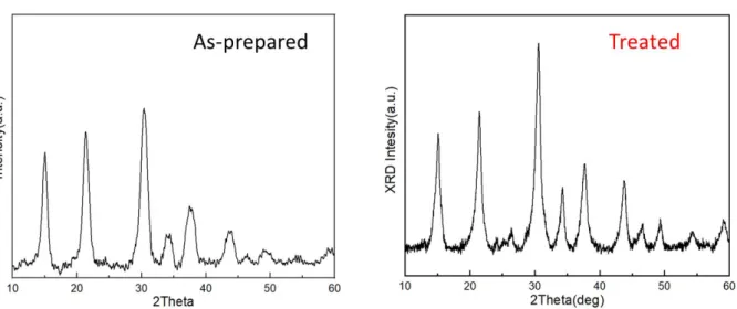
Characterization and measurements. XRD was carried out using a Bruker D8 ADVANCE diffractometer with Cu Ka (lambda=0.15406 nm) radiation. The surface morphology of NCs film was examined by SEM (FEI Nova Nano 630) and AFM (Bruker Dimension ICON), respectively. The absorbance spectrum was measured using an Evolution 600 ultraviolet– visible spectrophotometer (Thermo Scientific). PL measurement was conducted at room temperature using LabRAM ARAMIS Raman microscope (Horiba Scientific) with a 325 nm laser source as excitation. FET measurement was carried out using Keithley-4200 semiconductor characterization system.
Gas sensing tests. The sensor measurements were performed as follows. For any gas sensing measurements, the carrying gas was simulated air with volume ratio of N2 to O2 at 4 (BOC gas).
The gas flow rate was controlled by mass flow controllers (Bronkhorst) but kept the total gas flow rate at 0.5 L min-1. The analyte gases (ethanol, 9.91 ppm in N
2, Coregas; acetone, 10.1
ppm in N2, Coregas; methanol, 10 ppm in N2, BOC gas) were diluted to desired concentration
before purging into the chamber and the total gas flow rate was still kept at 0.5 L min-1.The
sample was loaded on a hotplate within a gas chamber (Linkam) and the temperature was controlled by a temperature controller. For the gas sensing measurements, two Au probes were separately placed on top of the two arms of CsPbBr3 NC thin film coated Pt interdigitated
electrode (DropSens) with an applied constant potential of 1 V. The dynamic gas sensing
response of CsPbBr3 NCs device was recorded by an electrochemical workstation (CHI 660E,
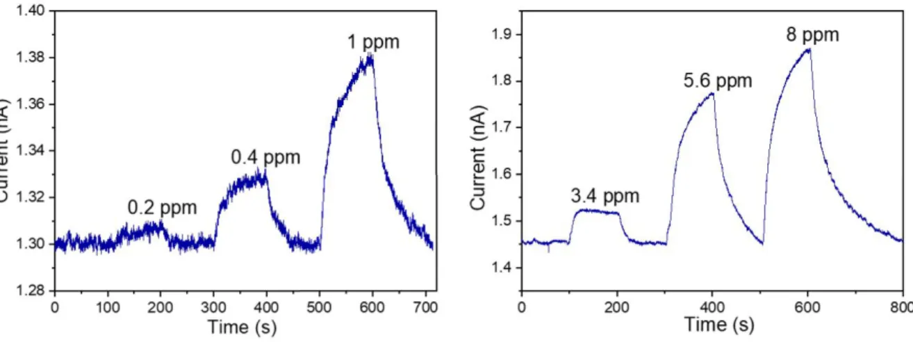
USA). The devices were taken out for the gas sensing measurements normally for about 1–2 h each time, and then stored in a dry desiccator for the rest of the time. The detection range of NO2 sensing measurement is from 0 to 8 ppm with the detection limit of 0.4 ppm.
Figure S1. SEM image of CsPbBr3 NCs films after soaking time 60 s (used in our work) and
300 s. The scale bars are 500 nm.
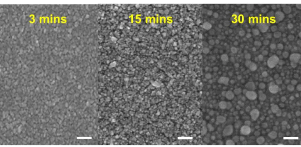
Figure S2. Top-view SEM image of CsPbBr3 NCs film ripened for 3, 15, and 30 mins,
Figure S3. Cross-section SEM image of the CsPbBr3 NCs films before and after ripening
with the scale bar of 100 nm.
400 450 500 550 600 650
P
L
In
te
n
si
ty
(a
.u
.)
Wavelength(nm)
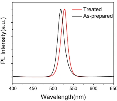
Treated As-preparedFigure S5. PL spectra of pristine and treated CsPbBr3 NCs thin films.
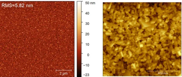
Figure S7. AFM image of the CsPbBr3 NC film.
Figure S9. Sensing response of CsPbBr3 NCs device with different NO2 concentration.
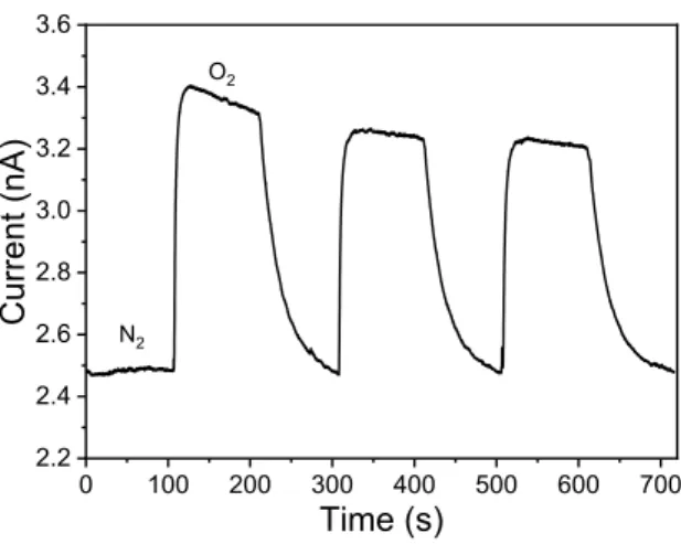
0 100 200 300 400 500 600 700 2.2 2.4 2.6 2.8 3.0 3.2 3.4 3.6 C ur re nt ( nA ) Time (s) N2 O2