MCP3909
Features
• Supports IEC 62053 International Energy Metering Specification
• Digital Waveform Data Access Through SPI Interface
- 16-bit Dual ADC Output Data Words - 20-bit Multiplier Output Data Word
• Dual Functionality Pins Support Serial Interface Access and Simultaneous Active Power Pulse Output
• Two 16-bit Second Order Delta-sigma Analog- to-Digital Converters (ADCs) with Multi-bit DAC - 81 dB SINAD (typical) on Both Channels • 0.1% Typical Active Energy Measurement Error
Over 1000:1 Dynamic Range
• PGA for Small Signal Input Supports Low Value Shunt Current Sensor
• Ultra-low Drift On-chip Reference,15 ppm/°C (typical)
• Direct Drive for Electromagnetic Mechanical Counter and Two-phase Stepper Motors • Low IDD of 4 mA (maximum)
• Tamper Output Pin for Negative Power Indication • Temperature Ranges:
- Industrial: -40°C to +85°C - Extended: -40°C to +125°C
Description
The MCP3909 device is an energy-metering IC designed to support the IEC 62053 international meter-ing standard specification. It supplies a frequency out-put proportional to the average active real power, with simultaneous serial access to ADC channels and mul-tiplier output data. This output waveform data is avail-able at up to 14 kHz with 16-bit ADC output and 20-bit multiplier output words. The 16-bit, delta-sigma ADCs allow for a wide range of IB and IMAX currents and/or small shunt (<200 µOhms) meter designs. A no-load threshold block prevents any current creep measure-ments for the active power pulse outputs. The integrated on-chip voltage reference has an ultra-low temperature drift of 15 ppm per degree C. This accurate energy metering IC with high field reli-ability is available in the industry standard 24-lead SSOP pinout.
Package Type
FOUT0 DGND NEG/SDO 1 2 3 4 24 23 22 21 20 19 18 17 5 6 7 8 FOUT1 NC CLKOUT CLKIN DVDD HPF AVDD NC CH0+ CH0- CH1-CH1+ HFOUT 16 9 G0 MCLR 15 14 10 11 G1 F0/CS REFIN/OUT AGND 13 12 F1/SDI F2/SCK 24-Lead SSOPMCP3909
Functional Block Diagram
16-bit ADC + – CH0+ CH0-Reference2.4V + – CH1+ CH1-HPF1 LPF1 DTF conversion REFIN/OUT FOUT1 HFOUT G0 G1 F2/SCK F1/SDI FOUT0 OSC1 OSC2 NEG/SDO HPF F0/CS Multi-level 16-bit ADC Multi-level X PGA Serial Control Buffers And Output Stepper Motor Output Drive Active Power SPI Interface Dual Functionality Pin
Control 20 16 16 16 16 MCLR Sub-systemClock for Active Power HPF1 4 k
MCP3909
1.0
ELECTRICAL
CHARACTERISTICS
Absolute Maximum Ratings †
VDD...7.0V Digital inputs and outputs w.r.t. AGND... -0.6V to VDD +0.6V Analog input w.r.t. AGND... ....-6V to +6V VREF input w.r.t. AGND... -0.6V to VDD +0.6V Storage temperature ...-65°C to +150°C Ambient temp. with power applied ...-65°C to +125°C Soldering temperature of leads (10 seconds) ... +300°C ESD on the analog inputs (HBM,MM) ... 5.0 kV, 500V ESD on all other pins (HBM,MM) ...5.0 kV, 500V
†Notice: Stresses above those listed under "Maximum Rat-ings" may cause permanent damage to the device. This is a stress rating only and functional operation of the device at those or any other conditions above those indicated in the operation listings of this specification is not implied. Exposure to maximum rating conditions for extended periods may affect device reliability.
ELECTRICAL CHARACTERISTICS
Electrical Specifications: Unless otherwise indicated, all parameters apply at AVDD = DVDD = 4.5V to 5.5V, Internal VREF, HPF turned on (AC mode), AGND, DGND = 0V, MCLK = 3.58 MHz; TA = -40°C to +85°C.
Parameter Sym Min Typ. Max Units Comment
Active Power Measurement Accuracy
Active Energy Measurement Error
E — 0.1 — % FOUT Channel 0 swings 1000:1 range,
FOUT0, FOUT1 Frequency outputs only, does not apply to serial interface data. (Note 1, Note 4)
No-Load Threshold/ Minimum Load
NLT — 0.0015 — % FOUT
Max
Frequency outputs only, does not apply to serial interface data. Disabled when F2, F1, F0 = 0, 1, 1
(Note 5, Note 6)
System Gain Error — 1 5 % FOUT (Note 2, Note 5)
AC Power Supply Rejection (output frequency variation)
AC PSRR — 0.01 — % FOUT F2, F1, F0 = 0, 1, 1 (Note 3)
DC Power Supply Rejection (output frequency variation)
DC PSRR — 0.01 — % FOUT HPF = 1, Gain = 1 (Note 3)
Waveform Sampling
A/D Converter Signal-to-Noise and Distortion Ratio
SINAD — 81 — dB Applies to both channels,
VIN = 0 dBFS at 50 Hz (VIN = Full Scale) Bandwidth
(Notch Frequency)
— 14 — kHz Applies to both channels,
MCLK/256 Phase Delay Between
Channels
— — 1/MCLK s HPF = 0 and 1, < 1 MCLK period
(Note 4, Note 6, Note 7)
Note 1: Measurement error = (Energy Measured By Device - True Energy)/True Energy * 100%. Accuracy is mea-sured with signal (±660 mV) on Channel 1. FOUT0, FOUT1 pulse outputs. Valid from 45 Hz to 75 Hz. See typical performance curves for higher frequencies and increased dynamic range. This parameter is not 100% production tested.
2: Does not include internal VREF. Gain = 1, CH0 = 470 mVDC, CH1 = 660 mVDC, difference between measured output frequency and expected transfer function.
MCP3909
ADC/PGA Specifications
Offset Error VOS — 2 5 mV Referred to Input, applies to both
channels
Gain Error Match — 0.5 — % FOUT (Note 5)
Internal Voltage Reference
Voltage — 2.4 — V Tolerance — ±2 — % Tempco — 15 — ppm/°C Reference Input Input Range 2.2 — 2.6 V Input Impedance 3.2 — — kΩ Input Capacitance — — 10 pF Analog Inputs
Maximum Signal Level — — ±1 V CH0+,CH0-,CH1+,CH1- to AGND
Differential Input Voltage Range Channel 0
— — ±470/G mV G = PGA Gain on Channel 0
Differential Input Voltage Range Channel 1
— — ±660 mV
Input Impedance 390 — — kΩ Proportional to 1/MCLK
Oscillator Input
Frequency Range MCLK 1 — 4 MHz
Power Specifications
Operating Voltage 4.5 — 5.5 V AVDD, DVDD
IDD,A IDD,A — 2.3 2.8 mA AVDD pin only
IDD,D IDD,D — 0.8 1.2 mA DVDD pin only
ELECTRICAL CHARACTERISTICS (CONTINUED)
Electrical Specifications: Unless otherwise indicated, all parameters apply at AVDD = DVDD = 4.5V to 5.5V, Internal VREF, HPF turned on (AC mode), AGND, DGND = 0V, MCLK = 3.58 MHz; TA = -40°C to +85°C.
Parameter Sym Min Typ. Max Units Comment
Note 1: Measurement error = (Energy Measured By Device - True Energy)/True Energy * 100%. Accuracy is mea-sured with signal (±660 mV) on Channel 1. FOUT0, FOUT1 pulse outputs. Valid from 45 Hz to 75 Hz. See typical performance curves for higher frequencies and increased dynamic range. This parameter is not 100% production tested.
2: Does not include internal VREF. Gain = 1, CH0 = 470 mVDC, CH1 = 660 mVDC, difference between measured output frequency and expected transfer function.
3: Percent of HFOUT output frequency variation; Includes external VREF = 2.5V, CH1 = 100 mVRMS @ 50 Hz, CH2 = 100 mVRMS @ 50 Hz, AVDD = 5V + 1 Vpp @ 100 Hz. DC PSRR: 5V ±500 mV
4: Error applies down to 60 degree lead (PF = 0.5 capacitive) and 60 degree lag (PF = 0.5 inductive).
5: Refer to Section 4.0 “Device Overview” for complete description.
6: Specified by characterization, not production tested.
MCP3909
TEMPERATURE CHARACTERISTICS
Electrical Specifications: Unless otherwise indicated, VDD = 4.5V to 5.5V, AGND, DGND = 0V.
Parameters Sym Min Typ Max Units Conditions
Temperature Ranges
Specified Temperature Range TA -40 — +85 °C
Operating Temperature Range TA -40 — +125 °C Note
Storage Temperature Range TA -65 — +150 °C
Thermal Package Resistances
Thermal Resistance, 24L-SSOP JA — 73 — °C/W
Note: The MCP3909 operates over this extended temperature range, but with reduced performance. In any case, the Junction Temperature (TJ) must not exceed the Absolute Maximum specification of +150°C.
TIMING CHARACTERISTICS
Electrical Specifications: Unless otherwise indicated, all parameters apply at AVDD = DVDD = 4.5V to 5.5V, AGND, DGND = 0V, MCLK = 3.58 MHz; TA = -40°C to +85°C.
Parameter Sym Min Typ Max Units Comment
Frequency Outputs
FOUT0 and FOUT1 Pulse Width (Logic Low)
tFW — 275 — ms 984376 MCLK periods
(Note 1)
HFOUT Pulse Width tHW — 90 — ms 322160 MCLK periods
(Note 2)
FOUT0 and FOUT1 Pulse Period tFP Refer to Equation 4-1 s
HFOUT Pulse Period tHP Refer to Equation 4-2 s
FOUT0 to FOUT1 Falling-Edge Time
tFS2 — 0.5 tFP —
FOUT0 to FOUT1 Minimum Sepa-ration
tFS — 4/MCLK —
Digital I/O
FOUT0 and FOUT1 Output High Voltage
VOH 4.5 — — V IOH = 10 mA, DVDD = 5.0V
FOUT0 and FOUT1 Output Low Voltage
VOL — — 0.5 V IOL = 10 mA, DVDD = 5.0V
HFOUT and NEG Output High Voltage
VOH 4.0 — — V IOH = 5 mA, DVDD = 5.0V
HFOUT and NEG Output Low Voltage
VOL — — 0.5 V IOL = 5 mA, DVDD = 5.0V
High-Level Input Voltage (All Digital Input Pins)
VIH 2.4 — — V DVDD = 5.0V
Low Level Input Voltage (All Digital Input Pins)
VIL — — 0.85 V DVDD = 5.0V
Input Leakage Current — 0.1 ±1 µA VIN = 0, VIN = DVDD
MCP3909
Serial Interface Timings (Note 4)
Data Ready Pulse Width tDR 4/MCLK
Reset Time tRST 100 — — ns
Output Data Rate fADC — MCLK/256 —
Serial Clock Frequency fCLK — 20 MHz VDD = 5V
Window for serial mode entry codes
tWINDOW — — 32/
MCLK
— Last bit must be clocked in before this time.
Window start time for serial mode entry codes
tWINSET 1/MCLK — — — First bit must be clocked in after this time.
Serial Clock High Time tHI — — 25 ns fCLK= 20 MHz
Serial Clock Low Time tLO — — 25 ns fCLK= 20 MHz
CS Fall to First Rising CLK Edge tSUCS 15 — — ns
Data Input Setup Time tSU 10 — — ns
Data Input Hold Time tHD — — 10 ns
CS Rise to Output Disable tDIS — — 150 ns
CLK Rise to Output Data Valid tDO — — 30 ns
SDO Rise Time tR — 2 — ns
SDO Fall Time tF — 2 — ns
TIMING CHARACTERISTICS (CONTINUED)
Electrical Specifications: Unless otherwise indicated, all parameters apply at AVDD = DVDD = 4.5V to 5.5V, AGND, DGND = 0V, MCLK = 3.58 MHz; TA = -40°C to +85°C.
Parameter Sym Min Typ Max Units Comment
Note 1: If output pulse period (tFP) falls below 984376*2 MCLK periods, then tFW = 1/2 tFP.
2: If output pulse period (tHP) falls below 322160*2 MCLK periods, then tHW = 1/2 tHP. When F2, F1, F0 equals 0,1,1, the HFOUT pulse time is fixed at 64 x MCLK periods or 18 µs for MCLK = 3.58 MHz.
3: Specified by characterization, not production tested.
MCP3909
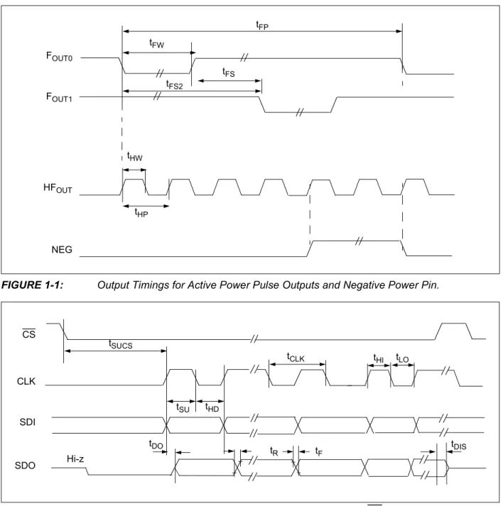
FIGURE 1-1: Output Timings for Active Power Pulse Outputs and Negative Power Pin.
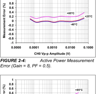
FIGURE 1-2: Serial Interface Timings showing Output, Rise, Hold, and CS Times. FOUT0 tFP FOUT1 HFOUT tFW tHP tHW tFS tFS2 NEG CS CLK SDI tSU tHD tSUCS tHI tLO SDO tDO tR tF tDIS tCLK Hi-z
MCP3909
FIGURE 1-3: SPI Output Pin Loading Circuit During SPI Testing. SPI Data Output Pin VDD 180 pF R VDD VOL– IOL ---= R VOH IOH ---=
MCP3909
2.0
TYPICAL PERFORMANCE CURVES
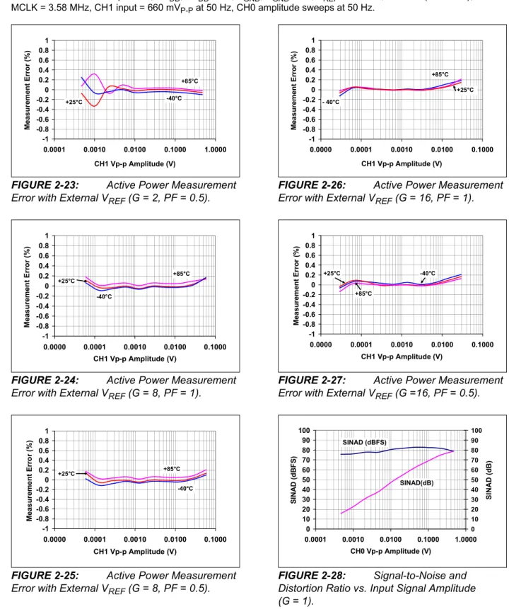
Note: Unless otherwise specified, DVDD, AVDD = 5V; AGND, DGND = 0V; VREF = Internal, HPF = 1 (AC mode), MCLK = 3.58 MHz, CH1 input = 660 mVP-P at 50 Hz, CH0 amplitude sweeps at 50 Hz.
FIGURE 2-1: Active Power Measurement
Error (Gain = 8, PF = 1).
FIGURE 2-2: Active Power Measurement
Error (Gain = 16, PF = 1).
FIGURE 2-4: Active Power Measurement
Error (Gain = 8, PF = 0.5).
FIGURE 2-5: Active Power Measurement
Error (Gain = 16, PF = 0.5).
Note: The graphs and tables provided following this note are a statistical summary based on a limited number of samples and are provided for informational purposes only. The performance characteristics listed herein are not tested or guaranteed. In some graphs or tables, the data presented may be outside the specified operating range (e.g., outside specified power supply range) and therefore outside the warranted range.
-1 -0.8 -0.6 -0.4 -0.2 0 0.2 0.4 0.6 0.8 1 0.0000 0.0001 0.0010 0.0100 0.1000 CH0 Vp-p Amplitude (V) Meas u remen t E rro r ( % ) +85°C +25°C -40°C ` -1 -0.8 -0.6 -0.4 -0.2 0 0.2 0.4 0.6 0.8 1 0.0000 0.0001 0.0010 0.0100 0.1000 CH0 Vp-p Amplitude (V) M ea su rem en t E rr o r ( % ) +85°C +25°C - 40°C -1 -0.8 -0.6 -0.4 -0.2 0 0.2 0.4 0.6 0.8 1 M e as ur em ent E rror ( % ) +85°C +25°C - 40°C -1 -0.8 -0.6 -0.4 -0.2 0 0.2 0.4 0.6 0.8 1 0.0000 0.0001 0.0010 0.0100 0.1000 CH0 Vp-p Amplitude (V) M ea su rem en t E rro r (% ) +85°C +25°C -40°C -1 -0.8 -0.6 -0.4 -0.2 0 0.2 0.4 0.6 0.8 1 0.0000 0.0001 0.0010 0.0100 0.1000 CH0 Vp-p Amplitude (V) M ea su rem en t E rr o r ( % ) +85°C +25°C -40°C -1 -0.8 -0.6 -0.4 -0.2 0 0.2 0.4 0.6 0.8 1 M e as ur em ent E rror ( % ) +85°C +25°C -40°C
MCP3909
Note: Unless otherwise specified, DVDD, AVDD = 5V; AGND, DGND = 0V; VREF = Internal, HPF = 1 (AC mode), MCLK = 3.58 MHz, CH1 input = 660 mVP-P at 50 Hz, CH0 amplitude sweeps at 50 Hz.
FIGURE 2-7: Active Power Measurement
Error (Gain = 1, PF = 1).
L
FIGURE 2-8: Active Power Measurement
Error (Gain = 1, PF = 0.5).
FIGURE 2-9: Measurement Error,
Temperature = +125°C, Gain = 1.
FIGURE 2-10: Measurement Error,
Temperature = +125°C, Gain = 2.
FIGURE 2-11: Measurement Error,
Temperature = +125°C, Gain = 8.
FIGURE 2-12: Measurement Error,
Temperature = +125°C, Gain = 16. -1 -0.8 -0.6 -0.4 -0.2 0 0.2 0.4 0.6 0.8 1 0.0001 0.0010 0.0100 0.1000 1.0000 CH0 Vp-p Amplitude (V) M e as ur em ent E rror ( % ) +85°C +25°C - 40°C -1 -0.8 -0.6 -0.4 -0.2 0 0.2 0.4 0.6 0.8 1 0.0001 0.0010 0.0100 0.1000 1.0000 CH0 Vp-p Amplitude (V) M e as ur em en t E rr o r (% ) +85°C +25°C -40°C -1 -0.8 -0.6 -0.4 -0.2 0 0.2 0.4 0.6 0.8 1 0.0001 0.001 0.01 0.1 1 CH1 V A lit d (V) Measurement Error (%) +25°C; PF = 1 +25°C; PF = 0.5 +125°C; PF = 0.5 +125°C; PF = 1 -1 -0.8 -0.6 -0.4 -0.2 0 0.2 0.4 0.6 0.8 1 0.0001 0.001 0.01 0.1 1 CH1 Vp-p Amplitude (V) Measurement Error (%) +25°C; PF = 1 +25°C; PF = 0.5 +125°C; PF = 1 +125°C; PF = 0.5 -1 -0.8 -0.6 -0.4 -0.2 0 0.2 0.4 0.6 0.8 1 0.0001 0.001 0.01 0.1 1 CH1 Vp-p Amplitude (V) Measurement Error (%) +125°C; PF = 1 +125°C; PF = 0.5 +25°C; PF = 1 +25°C; PF = 0.5 -1 -0.8 -0.6 -0.4 -0.2 0 0.2 0.4 0.6 0.8 1 0.0001 0.001 0.01 0.1 1 CH1 Vp-p Amplitude (V) Measurement Error (%) +25°C; PF = 1 +25°C; PF = 0.5 +125°C; PF = 1 +125°C; PF = 0.5
MCP3909
Note: Unless otherwise specified, DVDD, AVDD = 5V; AGND, DGND = 0V; VREF = Internal, HPF = 1 (AC mode), MCLK = 3.58 MHz, CH1 input = 660 mVP-P at 50 Hz, CH0 amplitude sweeps at 50 Hz.
FIGURE 2-13: Channel 0 Offset Error
(DC Mode, HPF off, G = 1, PF = 1).
FIGURE 2-14: Channel 0 Offset Error
(DC Mode, HPF off, G = 2, PF = 1).
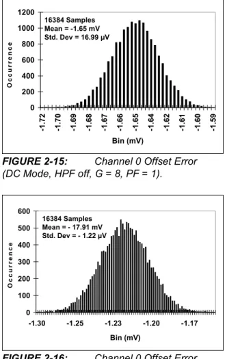
FIGURE 2-15: Channel 0 Offset Error
(DC Mode, HPF off, G = 8, PF = 1).
FIGURE 2-16: Channel 0 Offset Error
(DC Mode, HPF Off, G = 16, PF = 1). 0 500 1000 1500 2000 2500 3000 -1.77 -1.68 -1.59 -1.50 Bin (mV) O ccur a nc e 16,384 Samples Mean = -1.62 mV Std. Dev = 54.6 µV O c cu r r en c e 0 500 1000 1500 2000 2500 3000 -1 .3 0 -1 .2 7 -1 .2 5 -1 .2 2 -1 .2 0 -1 .1 8 -1 .1 6 -1 .1 3 -1 .1 1 Bin (mV) Oc cu ra nc e 16384 Samples Mean = -1.20 mV Std. Dev. = 25.1 µV O c cu r r en c e 0 200 400 600 800 1000 1200 -1. 7 2 -1. 7 0 -1. 6 9 -1. 6 8 -1. 6 7 -1. 6 6 -1. 6 5 -1. 6 4 -1. 6 2 -1. 6 1 -1. 6 0 -1. 5 9 Bin (mV) O ccu ra n ce 16384 Samples Mean = -1.65 mV Std. Dev = 16.99 µV O c cu r r en c e 0 100 200 300 400 500 600 -1.30 -1.25 -1.23 -1.20 -1.17 Bin (mV) Oc c u ra nc e 16384 Samples Mean = - 17.91 mV Std. Dev = - 1.22 µV O c cu r r en c e
MCP3909
Note: Unless otherwise specified, DVDD, AVDD = 5V; AGND, DGND = 0V; VREF = Internal, HPF = 1 (AC mode), MCLK = 3.58 MHz, CH1 input = 660 mVP-P at 50 Hz, CH0 amplitude sweeps at 50 Hz.
FIGURE 2-17: Active Power Measurement
Error over VDD, Internal VREF (G = 16, PF = 1).
FIGURE 2-18: Active Power Measurement
Error over VDD, External VREF (G = 1, PF = 1).
FIGURE 2-19: Active Power Measurement
Error vs. Input Frequency (G = 16).
FIGURE 2-20: Active Power Measurement
Error with External VREF (G = 1, PF = 1).
FIGURE 2-21: Active Power Measurement
Error with External VREF (G = 1, PF = 0.5).
FIGURE 2-22: Active Power Measurement
Error with External VREF (G = 2, PF = 1).
-0.15 -0.1 -0.05 0 0.05 0.1 0.15 0.2 0.25 0.3 0.0001 0.0010 0.0100 0.1000 1.0000 CH0 Vp-p Amplitude (V) M eas ur em ent Er ro r ( % ) VDD=4.75V VDD=5.0V VDD=4.5V VDD=5.25V VDD=5.5V -0.1 -0.05 0 0.05 0.1 0.15 0.2 0.0001 0.0010 0.0100 0.1000 1.0000 CH0 Vp-p Amplitude (V) Me a su re m en t E rro r (%) VDD=4.5V VDD=4.75V VDD=5.0V VDD=5.25V VDD=5.5V -0.5 -0.4 -0.3 -0.2 -0.1 0 0.1 0.2 0.3 0.4 0.5 45 50 55 60 65 70 75 Frequency (Hz) % Err o r PF = 0.5 PF = 1 -0.3 -0.2 -0.1 0 0.1 0.2 0.3 0.0001 0.0010 0.0100 0.1000 1.0000 CH0 Vp-p Amplitude (V) M eas ur em ent E rr o r ( % ) +85°C +25°C - 40°C -1 -0.8 -0.6 -0.4 -0.2 0 0.2 0.4 0.6 0.8 1 0.0001 0.0010 0.0100 0.1000 1.0000 CH1 Vp-p Amplitude (V) Meas ur e m en t E rr o r (% ) +85°C +25°C -40°C -0.5 -0.4 -0.3 -0.2 -0.1 0 0.1 0.2 0.3 0.4 0.5 0.0001 0.0010 0.0100 0.1000 1.0000 CH0 Vp-p Amplitude (V) M ea s u re m e n t Erro r (% ) +85°C +25°C - 40°C
MCP3909
Note: Unless otherwise specified, DVDD, AVDD = 5V; AGND, DGND = 0V; VREF = Internal, HPF = 1 (AC mode), MCLK = 3.58 MHz, CH1 input = 660 mVP-P at 50 Hz, CH0 amplitude sweeps at 50 Hz.
FIGURE 2-23: Active Power Measurement
Error with External VREF (G = 2, PF = 0.5).
FIGURE 2-24: Active Power Measurement
Error with External VREF (G = 8, PF = 1).
FIGURE 2-25: Active Power Measurement
Error with External VREF (G = 8, PF = 0.5).
FIGURE 2-26: Active Power Measurement
Error with External VREF (G = 16, PF = 1).
FIGURE 2-27: Active Power Measurement
Error with External VREF (G =16, PF = 0.5).
FIGURE 2-28: Signal-to-Noise and
Distortion Ratio vs. Input Signal Amplitude (G = 1). -1 -0.8 -0.6 -0.4 -0.2 0 0.2 0.4 0.6 0.8 1 0.0001 0.0010 0.0100 0.1000 1.0000 CH1 Vp-p Amplitude (V) Me as u rem en t E rr o r (% ) +85°C +25°C -40°C -1 -0.8 -0.6 -0.4 -0.2 0 0.2 0.4 0.6 0.8 1 0.0000 0.0001 0.0010 0.0100 0.1000 CH1 Vp-p Amplitude (V) M easu re m en t E rr o r ( % ) +85°C +25°C -40°C -1 -0.8 -0.6 -0.4 -0.2 0 0.2 0.4 0.6 0.8 1 0.0000 0.0001 0.0010 0.0100 0.1000 CH1 Vp-p Amplitude (V) Meas ur em e n t E rr o r (% ) +85°C +25°C -40°C -1 -0.8 -0.6 -0.4 -0.2 0 0.2 0.4 0.6 0.8 1 0.0000 0.0001 0.0010 0.0100 0.1000 CH1 Vp-p Amplitude (V) Meas ur e m en t E rr o r (% ) +85°C +25°C - 40°C -1 -0.8 -0.6 -0.4 -0.2 0 0.2 0.4 0.6 0.8 1 0.0000 0.0001 0.0010 0.0100 0.1000 CH1 Vp-p Amplitude (V) Me a s u re m en t Er ro r (% ) +85°C +25°C -40°C 0 10 20 30 40 50 60 70 80 90 100 0.0001 0.0010 0.0100 0.1000 1.0000 CH0 Vp-p Amplitude (V) S INA D (d B F S ) 0 10 20 30 40 50 60 70 80 90 100 SINAD (d B ) SINAD (dBFS) SINAD(dB)
MCP3909
Note: Unless otherwise specified, DVDD, AVDD = 5V; AGND, DGND = 0V; VREF = Internal, HPF = 1 (AC mode), MCLK = 3.58 MHz, CH1 input = 660 mVP-P at 50 Hz, CH0 amplitude sweeps at 50 Hz.
FIGURE 2-29: Signal-to-Noise and
Distortion Ratio vs. Input Signal Amplitude (G = 2).
FIGURE 2-30: Signal-to-Noise and
Distortion Ratio vs. Input Signal Amplitude (G = 8).
FIGURE 2-31: Signal-to-Noise and
Distortion Ratio vs. Input Signal Amplitude (G = 16).
FIGURE 2-32: Frequency Spectrum,
50 Hz Input Signal. 0 10 20 30 40 50 60 70 80 90 100 0.000100 0.001000 0.010000 0.100000 1.000000 CH0 Vp-p Amplitude (V) S INA D ( d B F S ) 0 10 20 30 40 50 60 70 80 90 100 SI NA D ( d B ) SINAD (dBFS) SINAD (dB) 0 10 20 30 40 50 60 70 80 90 100 0.00001 0.0001 0.001 0.01 0.1 CH0 Vp-p Amplitude (V) S INA D ( d B F S ) 0 10 20 30 40 50 60 70 80 90 100 SI NA D (d B) SINAD (dB) SINAD (dBFS) 0 10 20 30 40 50 60 70 80 90 100 0.000010 0.000100 0.001000 0.010000 0.100000 CH0 Vp-p Amplitude (V) S INA D ( d B F S ) 0 10 20 30 40 50 60 70 80 90 100 SI NA D ( d B ) SINAD (dBFS) SINAD (dB) -160 -140 -120 -100 -80 -60 -40 -20 0 0 2000 4000 6000 Frequency (Hz) A m pl it ud e ( d B )
MCP3909
3.0
PIN DESCRIPTIONS
The descriptions of the pins are listed in Table 3-1.
TABLE 3-1: PIN FUNCTION TABLE
3.1
Digital V
DD(DV
DD)
DVDD is the power supply pin for the digital circuitry within the MCP3909 device.
This pin requires appropriate bypass capacitors and should be maintained to 5V ±10% for specified operation. Refer to Section 6.0 “Applications Information”.
3.2
High-Pass Filter Input Logic Pin
(HPF)
HPF controls the state of the high-pass filter in both input channels. A logic ‘1’ enables both filters, remov-ing any DC offset comremov-ing from the system or the device. A logic ‘0’ disables both filters allowing DC voltages to be measured.
MCP3909
Symbol Description
SSOP
1 DVDD Digital Power Supply Pin
2 HPF High-Pass Filters Control Logic Pin
3 AVDD Analog Power Supply Pin
4 NC No Connect
5 CH0+ Non-Inverting Analog Input Pin for Channel 0 (Current Channel) 6 CH0- Inverting Analog Input Pin for Channel 0 (Current Channel) 7 CH1- Inverting Analog Input Pin for Channel 1 (Voltage Channel) 8 CH1+ Non-Inverting Analog Input Pin for Channel 1 (Voltage Channel)
9 MCLR Master Clear Logic Input Pin
10 REFIN/OUT Voltage Reference Input/Output Pin
11 AGND Analog Ground Pin, Return Path for internal analog circuitry 12 SCK / F2 Serial Clock or Frequency Control for HFOUT Logic Input Pin 13 SDI / F1 Serial Data Input or Frequency Control for FOUT0/1 Logic Input Pin 14 CS / F0 Chip Select or Frequency Control for FOUT0/1 Logic Input Pin
15 G1 Gain Control Logic Input Pin
16 G0 Gain Control Logic Input Pin
17 OSC1 Oscillator Crystal Connection Pin or Clock Input Pin
18 OSC2 Oscillator Crystal Connection Pin or Clock Output Pin
19 NC No Connect
20 SDO / NEG Serial Data Out or Negative Power Logic Output Pin 21 DGND Digital Ground Pin, Return Path for Internal Digital Circuitry 22 HFOUT High-Frequency Logic Output Pin (Intended for Calibration)
23 FOUT1 Differential Mechanical Counter Logic Output Pin
MCP3909
3.3
Analog V
DD(AV
DD)
AVDD is the power supply pin for the analog circuitry within the MCP3909.
This pin requires appropriate bypass capacitors and should be maintained to 5V ±10% for specified operation. Refer to Section 6.0 “Applications Information”.
3.4
Current Channel (CH0-, CH0+)
CH0- and CH0+ are the fully differential analog voltage input channels for the current measurement, containing a PGA for small-signal input, such as shunt current sensing. The linear and specified region of this channel is dependant on the PGA gain. This corresponds to a maximum differential voltage of ±470 mV/G and maxi-mum absolute voltage, with respect to AGND, of ±1V. Up to ±6V can be applied to these pins without the risk of permanent damage.Refer to Section 1.0 “Electrical Characteristics”.
3.5
Voltage Channel (CH1-,CH1+)
CH1- and CH1+ are the fully differential analog voltage input channels for the voltage measurement. The linear and specified region of these channels have a maxi-mum differential voltage of ±660 mV and a maximaxi-mum absolute voltage of ±1V, with respect to AGND. Up to±6V can be applied to these pins without the risk of per-manent damage.
Refer to Section 1.0 “Electrical Characteristics”.
3.6
Master Clear (MCLR)
MCLR controls the reset for both delta-sigma ADCs, all digital registers, the SINC filters for each channel and all accumulators post multiplier. The MCLR pin is also used to change pin functionality and enter the serial interface mode. A logic ‘0’ resets all registers and holds both ADCs in a Reset condition. The charge stored in both ADCs is flushed and their output is maintained to 0x0000h. The only block consuming power on the digital power supply during Reset is the oscillator circuit.
3.7
Reference (REFIN/OUT)
REFIN/OUT is the output for the internal 2.4V refer-ence. This reference has a typical temperature coeffi-cient of 15 ppm/°C and a tolerance of ±2%. In addition, an external reference can also be used by applying voltage to this pin within the specified range. This pin requires appropriate bypass capacitors to AGND, even when using the internal reference only.
Refer to Section 6.0 “Applications Information”.
3.8
Analog Ground (A
GND)
AGND is the ground connection to internal analog cir-cuitry (ADCs, PGA, band gap reference, POR). To ensure accuracy and noise cancellation, this pin must be connected to the same ground as DGND, preferably with a star connection. If an analog ground plane is available, it is recommended that this device be tied to this plane of the PCB. This plane should also reference all other analog circuitry in the system.
3.9
Serial Clock Input or F2 Frequency
Control Pin
This dual function pin can act as either the serial clock input for SPI communication or the F2 selection for the high-frequency output and low-frequency output pin ranges, changing the value of the constants FC and HFC used in the device transfer function. FC and HFC are the frequency constants that define the period of the output pulses for the device.
3.10
Serial Data Input or F1 Frequency
Control Pin
This dual function pin can act as either the serial data input for SPI communication or the F1 selection for the high-frequency output and low-frequency output pin ranges, changing the value of the constants FC and HFC used in the device transfer function. FC and HFC are the frequency constants that define the period of the output pulses for the device.
3.11
Chip Select (CS) or F0 Frequency
Control Pin
This dual function pin can act as either the chip select for SPI communication or the F0 selection for the high-frequency output and low-high-frequency output pin ranges by changing the value of the constants FC and HFC used in the device transfer function. FC and HFC are the frequency constants that define the period of the output pulses for the device.
3.12
Gain Control Logic Pins (G1, G0)
G1 and G0 select the PGA gain (G) on Channel 0 from four different values: 1, 2, 8 and 16.MCP3909
3.13
Oscillator (OSC1, OSC2)
OSC1 and OSC2 provide the master clock for the device. A resonant crystal or clock source with a similar sinusoidal waveform must be placed across these pins to ensure proper operation. The typical clock frequency specified is 3.579545 MHz. However, the clock fre-quency can be within the range of 1 MHz to 4 MHz without disturbing measurement error. Appropriate load capacitance should be connected to these pins for proper operation.
A full-swing, single-ended clock source may be con-nected to OSC1 with proper resistors in series to ensure no ringing of the clock source due to fast transient edges.
3.14
Serial Data Output or Negative
Power Output Logic Pin (NEG)
This dual function pin can act as either the serial data output for SPI communication or NEG. NEG detects the phase difference between the two channels and will go to a logic ‘1’ state when the phase difference is greater than 90° (i.e., when the measured real power is nega-tive). The output state is synchronous with the rising edge of HFOUT and maintains the logic ‘1’ until the real power becomes positive again and HFOUT shows a pulse.3.15
Ground Connection (D
GND)
DGND is the ground connection to internal digital circuitry (SINC filters, multiplier, HPF, LPF, digital-to-frequency converter and oscillator). To ensure accuracy and noise cancellation, DGND must be connected to the same ground as AGND, preferably with a star connection. If a digital ground plane is available, it is recommended that this device be tied to this plane of the Printed Circuit Board (PCB). This plane should also reference all other digital circuitry in the system.
3.16
High-Frequency Output (HF
OUT)
HFOUT is the high-frequency output of the device and supplies the instantaneous real-power information. The output is a periodic pulse output, with its period propor-tional to the measured real power, and to the HFC con-stant defined by F0, F1 and F2 pin logic states. This output is the preferred output for calibration due to faster output frequencies, giving smaller calibration times. Since this output gives instantaneous real power, the 2 ripple on the output should be noted. However, the average period will show minimal drift.3.17
Frequency Output (F
OUT0, F
OUT1)
FOUT0 and FOUT1 are the frequency outputs of the device that supply the average real-power information. The outputs are periodic pulse outputs, with its period proportional to the measured real power, and to the FC constant, defined by F0 and F1 pin logic states. These pins include high-output drive capability for direct use of electromechanical counters and 2-phase stepper motors. Since this output supplies average real power, any 2 ripple on the output pulse period is minimal.MCP3909
4.0
DEVICE OVERVIEW
The MCP3909 is an energy metering IC that serves two distinct functions that can operate simultaneously:
- Active Power Pulse Output - Waveform Output via SPI Interface
For the active power output, the device supplies a fre-quency output proportional to active (real) power, and higher frequency output proportional to the instantaneous power for meter calibration.
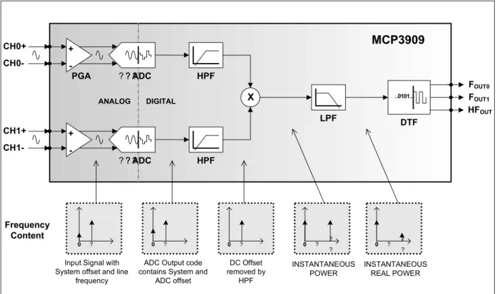
For the waveform output, it can be used serially to gather 16-bit voltage channel and current channel A/D data, or 20-bit wide multiplier output data. Both chan-nels use 16-bit, second-order, delta-sigma ADCs that oversample the input at a frequency equal to MCLK/4, allowing for wide dynamic range input signals. A Programmable Gain Amplifier (PGA) increases the usable range on the current input channel (Channel 0). Figure 4-1 represents the simplified block diagram of the MCP3909, detailing its main signal processing blocks.
Two digital high-pass filters cancel the system offset on both channels such that the real-power calculation does not include any circuit or system offset. After being high-pass filtered, the voltage and current signals are multiplied to give the instantaneous power signal. This signal does not contain the DC offset components, such that the averaging technique can be efficiently used to give the desired active-power output.
4.1
Active Power
The instantaneous power signal contains the active power information; it is the DC component of the instantaneous power. The averaging technique can be used with both sinusoidal and non-sinusoidal wave-forms, as well as for all power factors. The instanta-neous power is thus low-pass filtered in order to produce the instantaneous real-power signal.
A digital-to-frequency converter accumulates the instantaneous active real power information to produce output pulses with a frequency proportional to the average real power. The low-frequency pulses present at the FOUT0 and FOUT1 outputs are designed to drive electromechanical counters and two-phase stepper motors displaying the real-power energy consumed. Each pulse corresponds to a fixed quantity of real energy, selected by the F2, F1 and F0 logic settings. The HFOUT output has a higher frequency setting and less integration period such that it can represent the instantaneous real-power signal. Due to the shorter accumulation time, it enables the user to proceed to faster calibration under steady load conditions (see
Section 4.8 “Active Power FOUT0/1 and HFOUT Output Frequencies”). HPF ... 1 0 1 0 .. DTF -+ ? ?? ?ADC -+ PGA LPF HPF X CH0+ CH0-CH1+ CH1-? CH1-?CH1-? CH1-?ADC FOUT0 FOUT1 HFOUT INSTANTANEOUS POWER INSTANTANEOUS REAL POWER 0 ? 0 ?
MCP3909
DC Offset removed by ADC Output codecontains System and Input Signal with
System offset and line
0 ? ? ? 0 ? ? ? 0 ? Frequency Content ANALOG DIGITAL
MCP3909
4.2
Analog Inputs
The MCP3909 analog inputs can be connected directly to the current and voltage transducers (such as shunts or current transformers). Each input pin is protected by specialized ESD structures that are certified to pass 5 kV HBM and 500V MM contact charge. These struc-tures also allow up to ±6V continuous voltage to be present at their inputs without the risk of permanent damage.
Both channels have fully differential voltage inputs for better noise performance. The absolute voltage at each pin relative to AGND should be maintained in the ±1V range during operation in order to ensure the measure-ment error performance. The common-mode signals should be adapted to respect both the previous condi-tions and the differential input voltage range. For best performance, the common-mode signals should be referenced to AGND.
The current channel comprises a PGA on the front-end to allow for smaller signals to be measured without additional signal conditioning. The maximum differen-tial voltage specified on Channel 0 is equal to ±470 mV/ Gain (see Table 4-1). The maximum peak voltage specified on Channel 1 is equal to ±660 mV.
4.3
16-Bit Delta-Sigma A/D Converters
The ADCs used in the MCP3909 for both current and voltage channel measurements are delta-sigma ADCs. They comprise a second-order, delta-sigma modulator using a multi-bit DAC and a third-order SINC filter. The delta-sigma architecture is very appropriate for the applications targeted by the MCP3909 because it is a waveform-oriented converter architecture that can offer both high linearity and low distortion performance throughout a wide input dynamic range. It also creates minimal requirements for the anti-aliasing filter design. The multi-bit architecture used in the ADC minimizes quantization noise at the output of the converters without disturbing the linearity.Each ADC has a 16-bit resolution, allowing wide input dynamic range sensing. The oversampling ratio of both converters is 64. Both converters are continuously con-verting during normal operation. When the MCLR pin is low, both converters will be in Reset and output code 0x0000h. If the voltage at the inputs of the ADC is larger than the specified range, the linearity is no longer specified. However, the converters will continue to pro-duce output codes until their saturation point is reached. The DC saturation point is around 700 mV for Channel 0 and 1V for Channel 1, using internal voltage reference. The output code will be locked past the sat-uration point to the maximum output code.
The clocking signals for the ADCs are equally distrib-uted between the two channels in order to minimize phase delays to less than 1 MCLK period (see
Section 3.2 “High-Pass Filter Input Logic Pin (HPF)”). The SINC filters main notch is positioned at MCLK/256 (14 kHz with MCLK = 3.58 MHz), allowing the user to be able to measure wide harmonic content on either channel. The data ready signals used for syn-chronization of the part with a MCU will come at a rate of MCLK/256 and a pipeline delay of 3 data readys is required to settle the SINC 3rd order digital filter. The magnitude response of the SINC filter is shown in Figure 4-2.
FIGURE 4-2: SINC Filter Magnitude
Response (MCLK = 3.58 MHz).
TABLE 4-1: GAIN SELECTIONS
G1 G0 CH0 Gain CH0 VoltageMaximum
0 0 1 ±470 mV 0 1 2 ±235 mV 1 0 8 ±60 mV 1 1 16 ±30 mV -120 -100 -80 -60 -40 -20 0 0 5 10 15 20 25 30 Frequency (kHz) N o rm al Mo de R e jec tion ( d B )
MCP3909
4.4
Ultra-Low Drift V
REFThe MCP3909 contains an internal voltage reference source specially designed to minimize drift over tem-perature. This internal VREF supplies reference voltage to both current and voltage channels ADCs. The typical value of this voltage reference is 2.4V ±100 mV. The internal reference has a very low typical temperature coefficient of ±15 ppm/°C, allowing the output frequen-cies to have minimal variation with respect to tempera-ture since they are proportional to (1/VREF)².
The output pin for the voltage reference is REFIN/OUT. Appropriate bypass capacitors must be connected to the REFIN/OUT pin for proper operation (seeSection 6.0 “Applications Information”). The voltage reference source impedance is typically 4 kΩ
which enables this voltage reference to be overdriven by an external voltage reference source.
If an external voltage reference source is connected to the REFIN/OUT pin, the external voltage will be used as the reference for both current and voltage channel ADCs. The voltage across the source resistor will then be the difference between the internal and external voltage. The allowed input range for the external volt-age source goes from 2.2V to 2.6V for accurate mea-surement error. A VREF value outside of this range will cause additional heating and power consumption due to the source resistor, which might affect measurement error.
4.5
Power-On Reset (POR)
The MCP3909 contains an internal POR circuit that monitors analog supply voltage AVDD during operation. This circuit ensures correct device startup at system power-up and system power-down events. The POR circuit has built-in hysteresis and a timer to give a high degree of immunity to potential ripple and noise on the power supplies, allowing proper settling of the power supply during power-up. A 0.1 µF decoupling capacitor should be mounted as close as possible to the AVDDpin, providing additional transient immunity (seeSection 6.0 “Applications Information”). The threshold voltage is typically set at 4V, with a toler-ance of about ±5%. If the supply voltage falls below this threshold, the MCP3909 will be held in a Reset condi-tion (equivalent to applying logic ‘0’ on the MCLR pin). The typical hysteresis value is approximately 200 mV in order to prevent glitches on the power supply. Once a power-up event has occurred, an internal timer prevents the part from outputting any pulse for approx-imately 1s (with MCLK = 3.58 MHz), thereby prevent-ing potential metastability due to intermittent resets caused by an unsettled regulated power supply. Figure 4-3 illustrates the different conditions for a
FIGURE 4-3: Power-On Reset Operation.
4.6
High-Pass Filters and Multiplier
The active real-power value is extracted from the DC instantaneous power. Therefore, any DC offset compo-nent present on Channel 0 and Channel 1 affects the DC component of the instantaneous power and will cause the real-power calculation to be erroneous. In order to remove DC offset components from the instan-taneous power signal, a high-pass filter has been intro-duced on each channel. Since the high-pass filtering introduces phase delay, identical high-pass filters are implemented on both channels. The filters are clocked by the same digital signal, ensuring a phase difference between the two channels of less than one MCLK period. Under typical conditions (MCLK = 3.58 MHz), this phase difference is less than 0.005°, with a line fre-quency of 50 Hz. The cut-off frefre-quency of the filter (4.45 Hz) has been chosen to induce minimal gain error at typical line frequencies, allowing sufficient set-tling time for the desired applications. The two high-pass filters can be disabled by applying logic ‘0’ to the HPF pin.FIGURE 4-4: HPF Magnitude Response
(MCLK = 3.58 MHz). AVDD 5V 4.2V 4V 0V DEVICE MODE RESET PROPER OPERATION RESET NO PULSE OUT Time 1s -40 -35 -30 -25 -20 -15 -10 -5 0 0.1 1 10 100 1000 Frequency (Hz) N o rm a l M o de Re je ct io n (d B)
MCP3909
The multiplier output gives the product of the twohigh-pass filtered channels, corresponding to instanta-neous real power. Multiplying two sine wave signals by the same ω frequency gives a DC component and a 2ω component. The instantaneous power signal contains the real power of its DC component, while also contain-ing 2ω components coming from the line frequency multiplication. These 2ω components come for the line frequency (and its harmonics) and must be removed in order to extract the real-power information. This is accomplished using the low-pass filter and DTF converter.
4.7
Active Power Low-Pass Filter and
DTF Converter
For the active power signal calculation, the MCP3909 uses a digital low-pass filter. This low-pass filter is a first-order IIR filter, which is used to extract the active real-power information (DC component) from the instantaneous power signal. The magnitude response of this filter is detailed in Figure 4-5. Due to the fact that the instantaneous power signal has harmonic content (coming from the 2 components of the inputs), and since the filter is not ideal, there will be some ripple at the output of the low-pass filter at the harmonics of the line frequency.
The cut-off frequency of the filter (8.9 Hz) has been chosen to have sufficient rejection for commonly-used line frequencies (50 Hz and 60 Hz). With a standard input clock (MCLK = 3.58 MHz) and a 50 Hz line fre-quency, the rejection of the 2ω component (100 Hz) will be more than 20 dB. This equates to a 2ω component containing 10 times less power than the main DC com-ponent (i.e., the average active real power).
FIGURE 4-5: LPF1 Magnitude Response
(MCLK = 3.58 MHz).
The output of the low-pass filter is accumulated in the digital-to-frequency converter. This accumulation is compared to a different digital threshold for FOUT0/1 and HFOUT, representing a quantity of real energy mea-sured by the part. Every time the digital threshold on FOUT0/1 or HFOUT is crossed, the part will output a pulse (See Section 4.8 “Active Power FOUT0/1 and HFOUT Output Frequencies”).
The equivalent quantity of real energy required to out-put a pulse is much larger for the FOUT0/1 outputs than the HFOUT. This is such that the integration period for the FOUT0/1 outputs is much larger. This larger integra-tion period acts as another low-pass filter so that the output ripple due to the 2ω components is minimal. However, these components are not totally removed, since realized low-pass filters are never ideal. This will create a small jitter in the output frequency. Averaging the output pulses with a counter or a MCU in the appli-cation will then remove the small sinusoidal content of the output frequency and filter out the remaining 2
ripple.
HFOUT is intended to be used for calibration purposes due to its instantaneous power content. The shorter integration period of HFOUT demands that the 2ω com-ponent be given more attention. Since a sinusoidal sig-nal average is zero, averaging the HFOUT signal in steady-state conditions will give the proper real energy value. -40 -35 -30 -25 -20 -15 -10 -5 0 0.1 1 10 100 1000 Frequency (Hz) N o rma l M o d e R e je c tion ( d B )
MCP3909
4.8
Active Power F
OUT0/1and HF
OUTOutput Frequencies
The thresholds for the accumulated energy are differ-ent for FOUT0/1 and HFOUT (i.e., they have different transfer functions). The FOUT0/1 allowed output fre-quencies are quite low in order to allow superior inte-gration time (see Section 4.7 “Active Power Low-Pass Filter and DTF Converter”). The FOUT0/1 output frequency can be calculated with the following equation:
EQUATION 4-1: FOUT FREQUENCY
OUTPUT EQUATION
For a given DC input V, the DC and RMS values are equivalent. For a given AC input signal with amplitude of V, the equivalent RMS value is V/ sqrt(2), assuming purely sinusoidal signals. Note that since the real power is the product of two RMS inputs, the output fre-quencies of AC signals are half of the DC inputs ones, again assuming purely sinusoidal AC signals. The constant FC depends on the FOUT0 and FOUT1 digital settings. Table 4-2 shows FOUT0/1 output frequencies for the different logic settings.
The high-frequency output HFOUT has lower integra-tion times and, thus, higher frequencies. The output fre-quency value can be calculated with the following equation: FOUTHz 8.06 V 0V1G F C VREF 2 ---= Where:
V0 = the RMS differential voltage on Channel 0
V1 = the RMS differential voltage on Channel 1
G = the PGA gain on Channel 0 (current channel)
FC = the frequency constant selected VREF = the voltage reference
TABLE 4-2: ACTIVE POWER OUTPUT FREQUENCY CONSTANT FC FOR FOUT0/1 (VREF= 2.4V)
F1 F0 FC (Hz) FC (Hz) (MCLK = 3.58 MHz) FOUT Frequency (Hz) with Full-Scale DC Inputs FOUT Frequency (Hz) with Full-Scale AC Inputs 0 0 MCLK/221 1.71 0.74 0.37 0 1 MCLK/220 3.41 1.48 0.74 1 0 MCLK/219 6.83 2.96 1.48 1 1 MCLK/218 13.66 5.93 2.96
MCP3909
EQUATION 4-2: ACTIVE POWER HFOUT
FREQUENCY OUTPUT EQUATION
The constant HFC depends on the FOUT0 and FOUT1
digital settings with the Table 4-3.
The detailed timings of the output pulses are described in the Timing Characteristics table (see Section 1.0 “Electrical Characteristics” and Figure 1-1).
4.8.1 MINIMAL OUTPUT FREQUENCY
FOR NO-LOAD THRESHOLD
The MCP3909 also includes, on each output fre-quency, a no-load threshold circuit that will eliminate any creep effects in the meter. The outputs will not show any pulse if the output frequency falls below the no-load threshold. This threshold only applies to the pulse outputs and does not gate any serial data coming from either the A/D output or the multiplier output. The minimum output frequency on FOUT0/1 and HFOUT is equal to 0.0015% of the maximum output frequency (respectively FC and HFC) for each of the F2, F1 and F0 selections (see Table 4-2 and Table 4-3); except when F2, F1, F0 = 011. In this last configuration, the no-load threshold feature is disabled. The selection of FC will determine the start-up current load. In order to respect the IEC standards requirements, the meter will have to be designed to allow start-up currents compatible with the standards by choosing the FC value matching these requirements. For additional applications infor-mation on no-load threshold, startup current and other meter design points, refer to AN994, "IEC Compliant Active Energy Meter Design Using The MCP3905/6”, (DS00994).
TABLE 4-3: OUTPUT FREQUENCY CONSTANT HFC FOR HFOUT (VREF= 2.4V)
HFOUTHz 8.06V0V1GHFC VREF 2 ---= Where:
V0 = the RMS differential voltage on Channel 0
V1 = the RMS differential voltage on Channel 1
G = the PGA gain on Channel 0 (current channel)
HFC = the frequency constant selected VREF = the voltage reference
F2 F1 F0 HFC HFC (Hz) HFC (Hz)
(MCLK = 3.58 MHz)
HFOUT Frequency (Hz) with full scale AC Inputs
0 0 0 64 x FC MCLK/215 109.25 27.21 0 0 1 32 x FC MCLK/215 109.25 27.21 0 1 0 16 x FC MCLK/215 109.25 27.21 0 1 1 2048 x FC MCLK/27 27968.75 6070.12 1 0 0 128 x FC MCLK/216 219.51 47.42 1 0 1 64 x FC MCLK/216 219.51 47.42 1 1 0 32 x FC MCLK/216 219.51 47.42 1 1 1 16 x FC MCLK/216 219.51 47.42
MCP3909
5.0
SERIAL INTERFACE
DESCRIPTION
5.1
Dual Functionality Pin And Serial
Interface Overview
The MCP3909 device contains three serial modes that are accessible by changing the pin functionality of the NEG, F2, F1, and F0 pins to SDO, SCK, SDI and CS, respectively.
These modes are entered by giving the MCP3909 device a serial command on these pins during a time window after device reset or POR. During this window of time, F2 acts as SCK, F1 acts as SDI and F0 acts as CS. Once a serial mode has been entered, the device must be reset to disable mode functionality, or change to another serial mode. This is done by using MCLR pin or power on reset event.
During serial mode entry and the three serial modes, data is clocked into the device on the rising edge of SCK and out of the device on the falling edge of SCK. The SPI data can be access at up to 20 MHz. This speed enables quick data retrieval in between conver-sion times. For 3-phase metering applications with multiple ADCs, this fast communication is essential to allow for power calculation windows between conver-sions, as shown in Figure 5-3.
After a serial mode has been entered, all blocks of the MCP3909 device are still operational. The PGA, A/D converters, HPF, multiplier, LPF, and other digital sec-tions are still functional, allowing the device to have true dual functionality in energy metering systems.
FIGURE 5-1: Dual Functionality Pins for
the MCP3909. FOUT0 DGND NEG/SDO 1 2 3 4 24 23 22 21 20 19 18 17 5 6 7 8 FOUT1 NC CLKOUT CLKIN DVDD HPF AVDD NC CH0+ CH0- CH1-CH1+ HFOUT 16 9 G0 MCLR 15 14 10 11 G1 F0/CS REFIN/OUT AGND 13 12 F1/SDI F2/SCK tSAMPLE tLINE_CYC SDO DR
Phase A,B,C I & V Data
16 bits DR
tSAMPLE IRQ
IRQ
MCP3909
FIGURE 5-3: Dual Functionality Pin Serial Mode Entry Protocol.
5.2
Serial Mode Entry Codes
The MCP3909 devices contains three different serial modes with data presented in 2's complement coding. • Multiplier Output
• Dual Channel Output • Filter Input
After entering any of these modes the active power calculation block is still functional and presents output pulses on FOUT0, FOUT1, and HFOUT. For this reason, the F2, F1, F0 output frequency selection constant can be changed with multiple command bytes for serial mode entry.
The command bytes to enter these modes are described in Table 5-1. D3 D2 D1 D0 D5 D4 D7 D6 1 2 3 4 5 6 7 8 MCLR tWINSET tWINDOW F1 / SDI F2 / SCK F0 / CS
TABLE 5-1: ENTRY CODES
Command
D7...D0 Serial Mode
Internal State of F2, F1, F0 Constants Frequency Selection During Serial Mode (1)
F2 F1 F0
1 0 1 0 0 0 0 1 Multiplier Output 0 F1 pin 1
1 0 1 0 1 0 0 1 Multiplier Output 1 F1 pin 1
1 0 1 0 0 1 0 0 Dual Channel Output Pre HPF1 0 F1 pin 1
1 0 1 0 1 1 0 0 Dual Channel Output Post HPF1 1 F1 pin 1
1 0 1 0 1 0 1 0 Filter Input 1 0 F0 pin
1 0 1 0 1 1 1 0 Filter Input 1 1 F0 pin
1 0 1 0 0 0 1 0 Filter Input 0 0 F0 pin
1 0 1 0 0 1 1 0 Filter Input 0 1 F0 pin
Leav-MCP3909
5.3
Multiplier Output Mode
Multiplier mode allows the user to retrieve the output of the multiplier on the MCP3909 device. Data is pre-sented in a 20 bit (19 bit + sign) protocol, MSB first. A data ready flag (DR) is output for every MCLK/256 clock cycles and a new multiplier output value is ready. If the multiplier value is not clocked out of the device it will be over-written. Data is clocked out on the rising edge of SCK.
EQUATION 5-1:
FIGURE 5-4: Multiplier Output Mode.
TABLE 5-2: MULTIPLIER OUTPUT MODE CODING
Binary Decimal 0 1 1 1 1 1 1 1 1 1 1 1 1 1 1 1 1 1 1 1 +524287 0 1 1 1 1 1 1 1 1 1 1 1 1 1 1 1 1 1 1 0 +524286 0 0 0 0 0 0 0 0 0 0 0 0 0 0 0 0 0 0 0 0 0 1 1 1 1 1 1 1 1 1 1 1 1 1 1 1 1 1 1 1 1 -1 1 0 0 0 0 0 0 0 0 0 0 0 0 0 0 0 0 0 0 1 -524287 1 0 0 0 0 0 0 0 0 0 0 0 0 0 0 0 0 0 0 0 -524288
Multiplier Code
CH
0
+CH
0
––
CH
1
+–
CH
1
–
V
REF2
---
524288 8.06
G
=
F1 / SDI D3 D2 D1 D0 Hi-z Hi-z D16 D17 1 2 3 17 18 19 20 Hi-z X 20 X 20 4 DR D19 D18 0 F2 / SCK NEG / SDO F0 / CS SIGN MSB LSBMCP3909
5.4
Dual Channel Output Mode
This mode allows the user to retrieve the individual channel information from the ADC outputs. The ADC outputs of both channels are synchronized together and their data ready is represented by the data ready pulse on SDO. If the ADC output values are not clocked out of the device, they will be over-written. A 32-bit data word is given, each channel is 16 bits (15 bits + sign), presented in 2's complement coding. Channel 1 comes first then channel 0.
A data ready flag (DR) is output for every MCLK / 256 clock cycles and a new filter output value is ready. If the dual channel output values are not clocked, and is not clocked out of the device, they will be over-written. The following formulas relate the channel input volt-ages to their respective output code. The code locks to +32767 on the positive side, and to -32768 on the negative side.
EQUATION 5-2:
5.5
High-Pass Filter Control
There are two options for the channel output data. The first options collects the channel data pre-high pass filter, or the output of the SINC filter of the delta sigma modulator. The second option collects the channel data post high pass filter. It is important to note that the HPF pin controls the state of the high pass filter for this second option. If the HPF pin is low, the post high pass filter mode will output all zero's. This HPF pin must be
Channel 1 Code VIN+ VIN-– VREF --- 32768 8.06 0.47 0.66 --- =
Channel 0 Code VIN+ VIN-– VREF --- 32768 8.06 0.66 0.47 --- PGA =
TABLE 5-3: CHANNEL OUTPUT MODE
CODING Binary Decimal 0 111 1111 1111 1111 + 32,767 0 111 1111 1111 1110 + 32,766 0 000 0000 0000 0000 0 1 111 1111 1111 1111 -1 1 000 0000 0000 0001 - 32,767 1 000 0000 0000 0000 - 32,768
MCP3909
FIGURE 5-5: Dual Channel Output Mode.
5.6
Filter Input Mode
The filter input mode allows the user to feed the MCP3909 device an input to the LPF1. Data is received MSB first. The MCP3909 will treat this data as if it were the output of the multiplier and will LPF and D-F the result as normal, giving the resulting out-put frequency on HFOUT, FOUT0 and FOUT1. See Tables 4-2 and4-3 for transfer functions of the output frequencies.
When using filter input mode, the user must wait for the data ready flag (DR) to appear on SDO before attempting to clock in data to the device. The user can not access either the multiplier output or the dual channel output while in this mode.
FIGURE 5-6: Filter Input Mode.
D15 D14 D1 D0 Hi-z Hi-z D16 D17 1 2 15 17 18 31 32 Hi-z X 32 X 32 16 DR D31 D30 F1 / SDI F2 / SCK NEG / SDO F0 / CS X 16 X 16 X 16 X 16 Channel 1 Channel 0 D3 D2 D1 D0 Hi-z D16 D18 D17 1 2 3 17 18 19 20 X 20 X 20 4 D19 Hi-z DR F1 / SDI F2 / SCK NEG / SDO F0 / CS
MCP3909
5.7
Using the MCP3909 with
Microcontroller (MCU) SPI Ports
With microcontroller SPI ports, it is required to send groups of eight bits. It is also required that the micro-controller SPI port be configured to clock out data on the falling edge of clock and latch data in on the rising edge, or vice versa depending on the mode.5.7.1 SPI MODE DEFINITIONS
The following table represents the standard SPI mode terminology, the respective PIC bit settings, and a description of compatibility for the MCP3909 device. The MCP3909 works in SPI mode 0,1 mode, that is the data is clocked out of the part on the rising edge and clocked in on the falling edge of SCK.
TABLE 5-4: SPI MODE COMPATIBILITY
Standard SPI Mode Terminology
PIC Control Bits
State MCP3909
Compatibility Description
CKP CKE
0,0 0 1 — Idle state for clock is low level, transmit (from PIC)
occurs from active to idle clock state
0,1 0 0
√
Idle state for clock is low level, transmit (from PIC)occurs from idle to active clock state
1,0 1 1 — Idle state for clock is high level, transmit (from PIC)
occurs from active to idle clock state
1,1 1 0 — Idle state for clock is high level, transmit (from PIC)
MCP3909
FIGURE 5-7: Multiplier Output Mode 1 SPI Communication using 8-bit segments (Mode 0,1: SCK idles low).
1 2 3 4 5 6 7 8 9 10 11 12 13 14 15 16
D19 D15 D14 D13 D12 D11 D10 D9 D8 MCU latches data from
Data is clocked out on rising edges of SCK
Device on falling edges of SCK
Don’t Care X X X X X X X D15 D14 D13 D12 D11 D10 D9 D8 D19 D18 D17 D16 X X
MCU Transmit Buffer MCU Receive Buffer
X
Data is stored into the MCU receive register after transmission of the first 8 bits
Data is stored into the MCU receive register after transmission of the second 8 bits
D18 D17 D16 X X X X X 17 18 19 20 21 22 23 24 D2 D1 D0 X X D3 D2 D1 D0 X X
MCU Transmit Buffer MCU Receive Buffer
Data is stored into the MCU receive register after transmission of the third 8 bits
D3 X X X D7 D6 D5 D4 Don’t Care
X = Don’t Care Bits N = Null Bits 0 0 0 0 D7 D6 D5 D4 F1 / SDI F2 / SCK NEG / SDO F0 / CS F0 / CS F2 / SCK F1 / SDI NEG / SDO X X
MCP3909
FIGURE 5-8: Dual Channel Output Mode SPI Communication using 8-bit segments
(Mode 0,1: SCK idles low).
1 2 3 4 5 6 7 8 9 10 11 12 13 14 15 16
D14 D13 D12 D11 D7 D6 D5 D4 D3 D2 D1 D0 MCU latches data from
Data is clocked out on rising edges
Device on falling edges of SCK
Don’t Care
D7 D6 D5 D4 D3 D2 D1 D0 D11 D10 D9 D8
MCU Transmit Buffer MCU Receive Buffer
CH0 Data is stored into the MCU receive register after transmission of the first 8 bits
CH0 Data is stored into the MCU receive register after transmission of the second 8 bits
D15 D10 D9 D8
D15 D14 D13 D12
17 18 19 20 21 22 23 24 25 26 27 28 29 30 31 32 MCU latches data from
Data is clocked out on rising edges
Device on falling edges of SCK
Don’t Care
MCU Transmit Buffer MCU Receive Buffer
CH1 Data is stored into the MCU receive register after transmission of the third 8 bits
CH1 Data is stored into the MCU receive register after transmission of the fourth 8 bits
CHANNEL 0 CHANNEL 1 D14 D13 D12 D11 D7 D6 D5 D4 D3 D2 D1 D0 D15 D10 D9 D8 F1 / SDI F2 / SCK NEG / SDO F0 / CS F1 / SDI F2 / SCK NEG / SDO F0 / CS X X X X X X X X X X X X X X X X X X X X X X X X X X X X X X X X D7 D6 D5 D4 D3 D2 D1 D0 D11 D10 D9 D8 D15 D14 D13 D12