ELC 4383 RF/Microwave Circuits I
Laboratory 3: Optimization Using Advanced Design System Software
Note: This lab procedure has been adapted from a procedure written by Dr. Tom Weller at the University of South Florida for the WAMI program and from related procedures written for the WAMI Laboratory. It has been modified for use at Baylor University by Dr. Charles Baylis.
This laboratory exercise is a software exercise and should be completed individually (i.e. you will not have a lab partner).
Printed Name:
Please read the reminder on general policies and sign the statement below. Attach this page to your Post-Laboratory report.
General Policies for Completing Laboratory Assignments:
For each laboratory assignment you will also have to complete a Post-Laboratory report. For this report, you are strongly encouraged to collaborate with classmates and discuss the results, but the descriptions and conclusions must be completed individually. You will be graded primarily on the quality of the technical content, not the quantity or style of presentation. Your reports should be neat, accurate and concise (the Summary portion must be less than one page). Laboratory reports are due the week
following the laboratory experiment, unless notified otherwise, and should be turned in at the start of the laboratory period. See the syllabus and/or in-class instructions for additional instructions regarding the report format.
This laboratory report represents my own work, completed according to the guidelines described above. I have not improperly used previous semester laboratory reports, or cheated in any other way.
ELC 4383 – RF/Microwave Circuits I
Laboratory 3: Optimization Using Advanced Design System Software1 Laboratory Assignment:
Overview
This laboratory assignment provides an initial exposure to Advanced Design System (ADS), a software simulation tool from Agilent Technologies. In this exercise, two objectives will be accomplished:
1) Exposure to ADS
2) Equivalent Circuit Modeling
In this exercise, you will have the opportunity to represent a real-life inductor and capacitor by equivalent circuit models: more complicated circuit schematics that represent the “real” behavior of the circuit elements. This is an important part of the RF/microwave design process, as “real-life” elements contain non-idealities that influence frequency-dependent behavior. Parasitics, as these non-idealities are called, cause the behavior of a circuit element to deviate from its ideal behavior, usually at high frequencies. When the components to be used in building a design are modeled correctly, these non-idealities can be seen before the design is fabricated and necessary adjustments to produce desired circuit behavior can be made.
You will go through a session with the course instructor to introduce you to some of the basics of ADS. It should be kept in mind that ADS is a very complex simulator and its capabilities are enormous. The goal of this laboratory exercise is to familiarize you with some of the basic operations of the software.
Procedure
You will be modeling a 4.3 pF capacitor and a 16.0 nH inductor using “measured” data. You will need the following substrate parameters as you proceed through the simulations:
Substrate Parameters: H = 60 mils
Relative Dielectric Constant = 3.7 Loss Tangent = 0.003
Conductor Thickness = 1.7 mils Microstrip Taper Dimensions:
Capacitor: L = 72 mils, W1 = 138 mils, W2 = 28 mils Inductor: L = 72 mils, W1 = 138 mils, W2 = 27 mils
1
Dr. Tom Weller originally developed this laboratory procedure for the University of South Florida RF/Microwave Circuits I course and it was later modified by Dr. Charles Baylis for use at Baylor University. Parts of USF WAMI Lab Procedures 1, 2, 3, 6, and 10 were also used in constructing this assignment.
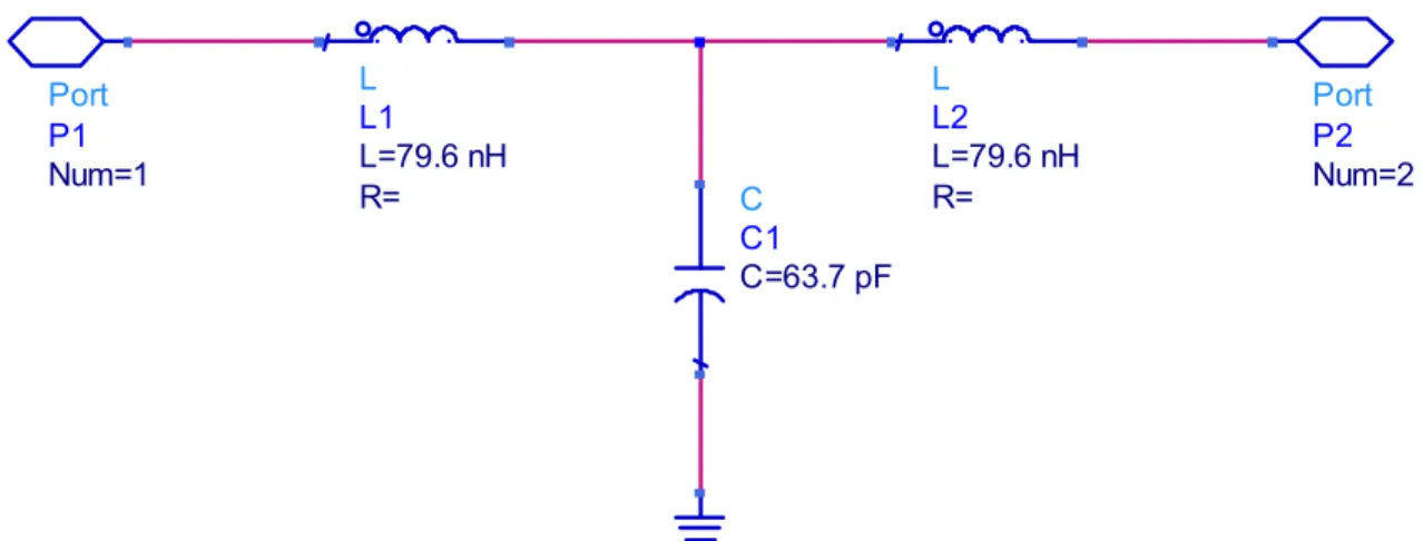
A. Construction and Simulation of a Lowpass Filter S_Param SP1 Step=0.01 GHz Stop=3 GHz Start=0.03 GHz S-PARAMETERS C C1 C=63.7 pF L L2 R= L=79.6 nH L L1 R= L=79.6 nH Term Term2 Z=50 Ohm Num=2 Term Term1 Z=50 Ohm Num=1
Figure 1: Ideal low pass filter with terminations.
1. Create a new project in ADS. Select File/New project. Click on the Browse button to find the home directory where you would like to store your project. Note that there should be no spaces in your project file path or file name. If there are spaces in the path or file name, ADS will report an error and will not save the project. Type in the project name. This title should end in _prj . Select Length Unit to be millimeters. Click OK.
2. On the left side of the schematic window, select the pull-down menu on the upper left of the screen and choose “Lumped Components” from the component palette. This allows different types of components to be placed in the schematic. Leave the setting on “Lumped Components.”
3. Click on the inductor in the Lumped Components palette. Then move the mouse into the schematic and place it on the schematic. You can press the Escape key when you have completed this task to end this function.
4. Double click on the inductor. Click on the ‘L’ parameter and modify its value to 79.6 nH. All of the remaining parameters are set correctly. Click OK to exit the menu.
5. Place a shunt capacitor to the right of the series inductor. You will have to use the Ctrl-R function to rotate the capacitor appropriately. Double-click on the capacitor and change the value of the ‘C’ parameter to 63.7 pF.
6. Add another 79.6 nH inductor in shunt to the right of the series capacitor. This completes the creation of a series-L, shunt-C, series-L filter.
7. The circuit will now be configured for S-parameter simulation. At the top left, change the palette to Simulation-S_Param. Click on “Term” and add two terminations to the network: the first should be at the left-hand side and the second should be at the right-hand side. Leave the Z setting at 50 Ohms for each termination.
8. Add an SP block from the same palette to the schematic. Double-click on the block and change the start frequency to 0.03 GHz, the stop frequency to 3.0 GHz, and the step to 0.01 GHz. The appropriate number of points will automatically appear as 298 points. Click Apply then OK to exit.
9. Click on the lowest bar of the menu immediately above the schematic on the ground symbol. Add a ground symbol below each of the terminations and also below the shunt capacitor.
10. There is a wire symbol on the same bar as the ground symbol. Use wire segments to connect all of the circuit elements appropriately. Your circuit should appear as the circuit shown in Figure 1.
11. Click on the Simulate button Shown Below in Figure 2. A popup window will appear to provide status updates on the simulation.
Figure 2: Simulate Button
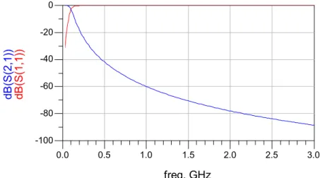
12. Following completion of the simulation, a data display window should automatically pop up. If it does not, the data display icon that is two icons to the right of the simulation icon can be selected. Choose the rectangular plot icon from the first row, second column of the plot palette and place this in the data display window. After it is placed, a pop-up window will provide options for placement in the graph. Select S(1,1) and click Add. Then select S(2,1) and click Add. Select dB from the popup window and click OK. Click OK again. The plot should appear as shown below:
0.5 1.0 1.5 2.0 2.5 0.0 3.0 -80 -60 -40 -20 -100 0 freq, GHz dB (S (1 ,1 )) dB (S (2 ,1 ))
You can print this plot by going to File Æ Print, or you can select it and paste the picture of the graph into a Word document. Provide this printout in your laboratory report and explain why the plot makes sense in terms of what you would expect from a low pass filter.
B. Referencing Sub-Circuits from a Higher Level Schematic
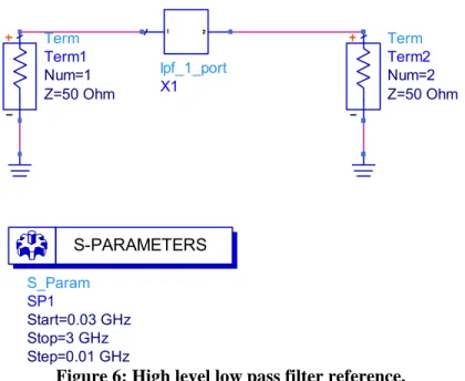
1. In Part A, terminations were used to obtain S-parameter simulation results. In this section, we will use “ports” to reference a circuit from a “higher-level” schematic. Take the low-pass filter design from Part A and save the design as lpf_1_port.dsn. Do not change the save path, ADS automatically saves all designs to the proper folder in the current project.
2. In lpf_1_port.dsn, remove the terminations and replace them with ports (available on the lower toolbar above the schematic). Remove the S-parameter simulation block. Save your design. The resulting schematic should look as follows:
Figure 4: Ideal low pass filter with input and output ports.
Port P2 Num=2 Port P1 Num=1 C C1 C=63.7 pF L L2 R= L=79.6 nH L L1 R= L=79.6 nH
3. Create a higher-level circuit called lpf_higherlevel.dsn. Click on the “Library Books” icon Æ Projects
Æ project name on the toolbar above the schematic, and select lpf_1_port. Right click the lpf_1_port and
select drop component then click to drop this two-port network in the schematic. Create the S-parameter simulation block as in Section A and run a simulation with the same frequency settings.
Figure 6: High level low pass filter reference. S_Param SP1 Step=0.01 GHz Stop=3 GHz Start=0.03 GHz S-PARAMETERS Term Term2 Z=50 Ohm Num=2 Term Term1 Z=50 Ohm Num=1 lpf_1_port X1
4. Plot the results and attach a printout to your laboratory report
C. Simulating Two Different Circuits Simultaneously in the Same Schematic Window
1. Create the following one-port circuit and save the design as matckt_fake.dsn. The transmission line
can be found in the Tlines-Ideal palette.
R
R1
R=100 Ohm
TLIN
TL1
F=2 GHz
E=90
Z=70.7 Ohm
Port
P1
Num=1
Figure 7: Ideal schematic for matcktb.dsn.
2. Change the load resistor value to 200 Ohms and the characteristic impedance of the transmission line
to 100 Ohms and save this circuit as matcktb_fake.
3. Create a higher-level schematic as matckt_lab. Use the library books icon to reference both of the
circuits from matckt_lab. Set up the following simulation. S11 will represent the input reflection coefficient to matckt_fake, and S22 will represent the input reflection coefficient to matcktb_fake.
Figure 8: High level schematic for matching circuits. S_Param SP1 Step=0.01 GHz Stop=3 GHz Start=30 kHz S-PARAMETERS Term Term2 Z=50 Ohm Num=2 Term Term1 Z=50 Ohm Num=1 matckt_fake X1 matcktb_fake X2
4. Run the simulation and plot the reflection coefficients on top of each other in a new display window by opening a graph and selecting both S(1,1) and S(2,2) in dB. Attach a plot to your laboratory report.
D. Equivalent Circuit Modeling of Capacitor
1. You will need to create a schematic that references 2-port S-parameter data in a .s2p file format. Open a new design window and title it “cap_data_4p3pf_xxx.dsn”, where xxx are your initials.
2. Now open the “Data Items” palette and place a two-port (S2P) box into the schematic. The box will have three “wires” to connect.
3. Using Windows Explorer, place the S-parameter data file for the 4.3 pF capacitor (CAP_035_R60_4p3.s2p) into the Data folder under your project directory.
4. Double click on the 2-port box and click “Browse” next to the File Name box. Select CAP_035_R60_4p3.s2p. Make sure the file type is Touchstone.
Port
P2
Num=2
Port
P1
Num=1
S2P
SNP1
File="CAP_035_R60_4p3.s2p"
2 1 RefFigure 9: Lower level capacitor model.
6. Create a new .dsn file. Call this file cap_model_4p3pF_xxx, where xxx are your initials. 7. Create the equivalent circuit model for the capacitor shown below in Figure 7. You will use transmission line elements and substrate (MTAPER, MSUB) from the Tlines-Microstrip palette and lumped circuit elements. Place a VAR block in the circuit from the toolbar immediately above the schematic. Use ports as shown.
Figure 10: Equivalent capacitor circuit model.
VAR VAR1 R1=1 {o} L1=1 {o} C3=0.1 {o} C2=1 {o} C1=4.3 {o} Eqn Var C C2 C=C1 pF MSUB MSub1 Rough=0 mm TanD=0.003 T=1.7 mil Hu=1.0e+033 mm Cond=1.0E+50 Mur=1 Er=3.7 H=60 mil MSub MTAPER Taper2 L=72 mil W2=28 mil W1=138 mil Subst="MSub1" MTAPER Taper1 L=72 mil W2=28 mil W1=138 mil Subst="MSub1" CC4 C=C2 pF C C3 C=C3 pF R R1 R=R1 Ohm L L1 R= L=L1 nH C C1 C=C2 pF Port P2 Num=2 Port P1 Num=1
8. Double-click on the VAR block. Select “Tune/Opt/Stat/DOE Setup”. This will allow you to set the optimization ranges for the model parameters. Set the optimization ranges as shown in the following schematic. Note that the initial value for C1 is 4.3 pF, the nominal capacitance value. The optimization ranges are shown below in Table 1.
Variable Initial Value Optimization Range C1 4.3 0 to 10 C2 1 0 to 2 C3 0.1 0 to 5 L1 1 0 to 5 R1 1 0 to 5
Table 1: Capacitor model variable initial and optimization values.
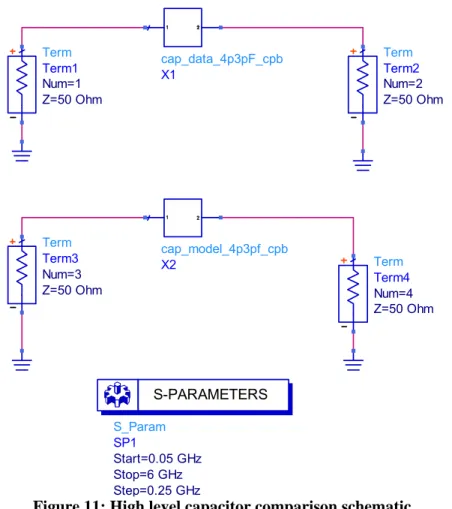
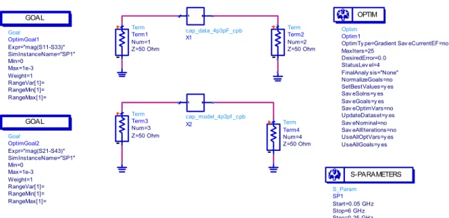
9. Create a higher level schematic named “cap_main_4p3pF”. Place references to the data and model
circuits in the schematic. Add an S-parameter simulation block to enable S-parameter simulations from 0.05 GHz to 6 GHz in steps of 0.25 GHz. The schematic should appear as follows:
Figure 11: High level capacitor comparison schematic.
S_Param SP1 Step=0.25 GHz Stop=6 GHz Start=0.05 GHz S-PARAMETERS cap_model_4p3pf_cpb X2 Term Term2 Z=50 Ohm Num=2 Term Term4 Z=50 Ohm Num=4 Term Term3 Z=50 Ohm Num=3 Term Term1 Z=50 Ohm Num=1 cap_data_4p3pF_cpb X1
10. Now add optimization capabilities. The goal is to adjust the parameters (capacitances, inductances, and resistances) of the equivalent circuit schematic to allow the S-parameter data generated by the model to match the measured S-parameter data as closely as possible. Select the Optimum/Stat/Yield/DOE palette and place two “Goals” blocks into the schematic. In addition, place an “Optim” block into the schematic.
Figure 12: High level capacitor comparison schematic with optimization blocks. Optim Optim1 Sav eCurrentEF=no UseAllGoals=y es UseAllOptVars=y es Sav eAllIterations=no Sav eNominal=no UpdateDataset=y es Sav eOptimVars=no Sav eGoals=y es Sav eSolns=y es SetBestValues=y es NormalizeGoals=no FinalAnaly sis="None" StatusLev el=4 DesiredError=0.0 MaxIters=25 OptimTy pe=Gradient OPTIM Goal OptimGoal2 RangeMax[1]= RangeMin[1]= RangeVar[1]= Weight=1 Max=1e-3 Min=0 SimInstanceName="SP1" Expr="mag(S21-S43)" GOAL Goal OptimGoal1 RangeMax[1]= RangeMin[1]= RangeVar[1]= Weight=1 Max=1e-3 Min=0 SimInstanceName="SP1" Expr="mag(S11-S33)" GOAL S_Param SP1 Step=0.25 GHz Stop=6 GHz Start=0.05 GHz S-PARAMETERS cap_model_4p3pf _cpb X2 Term Term2 Z=50 Ohm Num=2 Term Term4 Z=50 Ohm Num=4 Term Term3 Z=50 Ohm Num=3 Term Term1 Z=50 Ohm Num=1 cap_data_4p3pF_cpb X1
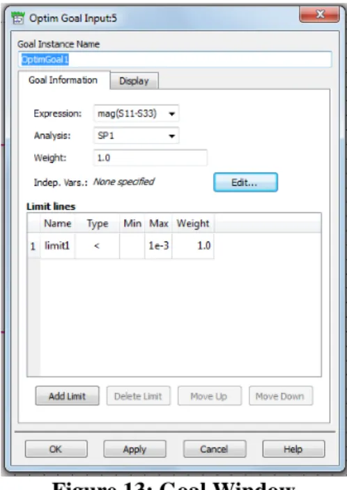
11. Double-click on the first Goal block. It is necessary to choose the expression that the optimizer will minimize. We would like to minimize the vector difference between S11 of the data circuit and S11 of the model circuit. S33 corresponds to S11 of the model circuit. Thus, type mag(S11-S33) in the “Expression” box of the Information tab in the Goal block dialog window.
12. Select SP1 as the Analysis.
13. Change the limit1 Type to inside and specify the Min as 0 and the Max as 1e-3; also, set the Weight as 1.
14. In the second goal block, minimize the vector difference between the S21 values of the measured and model data by entering “mag(S21-S43)” in the “Expression” area. Change limit1 type to inside and use a weight of 1.
Figure 13: Goal Window
15. Double click on the Optim block. Select the Setup tab and select Gradient from the “Optimization Type” pull-down menu. In many cases, it is best to perform a Random optimization first and then use gradient for fine-tuning (a good example of this is when you are not sure of the “ballpark” values of your equivalent circuit parameters). Usually gradient is used when you know you are reasonably close to your optimum solution.
16. As the “Stopping Criteria,” select 100 as the Number of Iterations.
17. Click Apply then OK to exit the window. The schematic should be the same as the schematic shown in Figure 9.
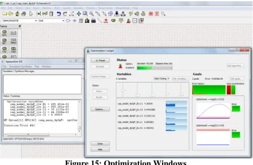
18. Before optimizing, de-activate the “OPTIM” block by use of the “X” that is the second command from left on the upper toolbar above the schematic window. Then perform an S-parameter simulation to view the comparison between the measurement data and the model before optimization. Set up two rectangular plots: one showing measurement versus model data for |S11| in dB and measured versus model data for |S21| in dB, and a second comparing the phase of S11 and S21. Attach these plots to your report.
19. Now activate the “OPTIM” block and click the optimize button. The optimization will be performed. The optimization cockpit window will be similar to that shown in Figure 15.
Figure 14: Optimize Button
20. After the optimization is complete, click “Update Design” in the optimization cockpit window. Notice that the variable values shown in this window are different from the initial values specified in the
Figure 15: Optimization Windows
21. Examine the parameter values. If any of the parameter values is close to a limit, click “edit
variables” in the optimization cockpit and adjust the limit values. Next, deactivate the OPTIM block, and simulate. View the simulation plots, and if the results are not acceptable, activate the OPTIM block run the optimization again. Continue until excellent correspondence between measured and model data is achieved. Provide the final values of your parameters in your report.
To summarize, you should provide the following for the capacitor results: 1) Schematics for data, model, and upper level simulation
2) Comparisons of S11 (dB and phase) and S21 (dB and phase) for initial values and final optimized values
3) Final optimized equivalent circuit model parameter values
E. Equivalent Circuit Modeling of Inductor
Repeat the steps to set up an optimization for the 16.0 nH inductor. Your starting equivalent circuit model for the inductor should appear as follows. All substrate and taper line parameters are the same as for the capacitor. The optimization ranges are as follows shown below in Table 2.
Figure 10: Equivalent inductor model schematic. VAR VAR1 R1=1 {o} L1=16.0 {o} C3=0.1 {o} C2=1 {o} Eqn Var L L1 R= L=L1 nH MSUB MSub1 Rough=0 mm TanD=0.003 T=1.7 mil Hu=1.0e+033 mm Cond=1.0E+50 Mur=1 Er=3.7 H=60 mil MSub MTAPER Taper2 L=72 mil W2=28 mil W1=138 mil Subst="MSub1" MTAPER Taper1 L=72 mil W2=28 mil W1=138 mil Subst="MSub1" CC4 C=C2 pF C C3 C=C3 pF R R1 R=R1 Ohm C C1 C=C2 pF Port P2 Num=2 Port P1 Num=1 Variable Initial Value Optimization Range C2 1 0 to 2 C3 0.1 0 to 2 L1 16 0 to 30 R1 1 0 to 5
Table 2: Inductor model variable and optimization values
Provide the following for your report:
To summarize, you should provide the following for the capacitor results: 1) Schematics for data, model, and upper level simulation
2) Comparisons of S11 (dB and phase) and S21 (dB and phase) for initial values and final optimized values
3) Final optimized equivalent circuit model parameter values
For Your Report:
SUMMARY – As usual, provide a summary of no more than one-half page describing the laboratory. DISCUSSION OF RESULTS:
(1) How do the actual measured results for a capacitor compare to the results you would expect for an ideal capacitor? What about for the inductor?
(2) Attempt to make some correlations between physical construction of the components and their equivalent circuit models.