V. N. Kushnir,1S. L. Prischepa,1C. Cirillo,2A. Vecchione,2C. Attanasio,2M. Yu. Kupriyanov,3and J. Aarts4
1State University of Informatics and RadioElectronics, P. Browka 6, Minsk 220013, Belarus
2CNR-SPIN Salerno and Dipartimento di Fisica “E.R. Caianiello”, Universit`a degli Studi di Salerno, Fisciano (Sa) IT-84084, Italy 3Nuclear Physics Institute, Moscow State University, Moscow 119992, Russia
4Kamerlingh Onnes Laboratory, Leiden University, P.O. Box 9504, NL-2300 RA Leiden, The Netherlands
(Received 13 June 2011; revised manuscript received 10 October 2011; published 7 December 2011) The coupling of two superconductors (S) through a ferromagnet (F) can lead to either a zero- or aπ-phase difference between the superconducting banks. Most research in this area is performed on trilayer S/F/S film structures, in which two-order parameter configurations are possible. Increasing the number of layers and junctions leads to a larger number of possible configurations with, in principle, different properties such as the superconducting transition temperatureTc. Here we study the behavior of a series of multilayers made of superconducting Nb and ferromagnetic Pd81Ni19. We find that for the individual layer thicknesses used, the
transition widthTcincreases with increasing number of bilayers in the multilayer, in a well-defined manner. That the broadening is not simply due to increased disorder in the larger stacks, it is shown from x-ray diffraction, which finds very sharp interfaces for all samples; and from the effect of the magnetic field on the transition, which shows a considerable sharpening. We can make a connection with the various order parameter configurations using a matrix formulation of quasiclassical theory based on the Usadel equations and show that these different configurations take part in the Josephson networks, which are building up in the transition to the superconducting state.
DOI:10.1103/PhysRevB.84.214512 PACS number(s): 74.78.Fk, 74.45.+c
I. INTRODUCTION
When combining a superconducting (S) and a ferromag-netic (F) thin film, it is well known that the superconduct-ing correlations induced in the ferromagnet are spatially inhomogeneous.1 In SFS junctions, by choosing the appro-priate value for the F-layer thicknessdF, this can lead to a
so-calledπstate, in which the phase of the superconducting order parameter changes overπ when going from one side of the junction to the other. This is by now a well-established effect, with experimental consequences such as strong variations of the junction critical current as a function of temperature,2or spontaneous currents occurring in a superconducting ring with an SFS junction.3 Obviously the SFS trilayer can only have two ground states: one without phase change, and one with a phase change (equivalent to a sign change or a node) in the pair amplitude. The two states have a different critical temperature Tc, leading to the well-known Tc oscillations as function of
dF.4When more junctions are added to the stack, the number
of possible modes can be expressed in terms of a primary building block1
2dF/dS/ 1
2dF(withdSthe S-layer thickness) as
Ntri+1, whereNtri is the number of blocks. More than one
node is now possible, which distinguishes the S/F case from multilayers with normal metals, and S/F multilayers from an SFS trilayer. Each mode can be characterized by its own critical temperature. A first attempt to clarify such new issues was recently published.5Incidentally, forTcthe well-known limit
to the problem is the infinite multilayer (IM) with periodic boundary conditions. With this approach, calculations were for instance made of the upper critical field behavior in S/N superlattices,6 while for the F case it actually led to the prediction of oscillatory Tc(dF).7,8 On general grounds, the
infinite multilayer Tc with a symmetrical periodic solution
furnishes the upper limit forTcof a system with a finite number
of blocks.
In this work we compare the nucleation of superconduc-tivity in samples with different symmetries, where different modes can play a weaker or a stronger role. For the preparation we use weakly ferromagnetic Pd81Ni19 and superconducting
Nb, and choose a valuedF somewhat lower than the value
where the 0–π transition in a simple S/F/S junction is expected.9In particular we compare samples with fixedd
F,dS,
and IM symmetry, consisting ofNtri building blocks defined above, with samples consisting of a starting F layer and Nbi(F/S) bilayers{notation [F/Nbi(S/F)]}. Such samples we
call asymmetric in the sense that they do not possess the IM symmetry, even though they possess a mirror plane. A sketch of both types of multilayers is given in Fig.1. We find that this difference in symmetry (where actually only the outer layers have different thicknesses) has clearly observable effects on the nucleation, both seen in the width of the resistive transition Tc and in its shape. For the symmetric samples, Tc is
small (≈50 mK) and hardly changes with increasing Ntri.
For the asymmetric samples, Tc gradually increases until
a maximum width of around 2 K is reached aroundNbi=9,
after which it becomes constant. We also find the occurrence of steps in the resistance. In one particular sample withNbi=9,
the number of steps even comes close to the number of possible modesNbi. However, in a magnetic field the broad transitions sharpen up again. Next we demonstrate that both the increasing Tc as well as its final value can be directly connected to
the increasing number of modes. For this we use a matrix formulation of the quasiclassical theory on basis of the Usadel equation. We use measurements on bilayer building blocks as input parameters, calculate theTc values of the different
modes, and extract in this way a highest and lowest value ofTc
for a multilayer, which can be connected to the measuredTc.
V. N. KUSHNIRet al. PHYSICAL REVIEW B84, 214512 (2011)
F S F S F S F Z
X
0
dS dS dS
dF/2 dF dF dF/2
F S F S F S F Z
X
0
dS dS dS
dF dF dF dF
FIG. 1. Left: symmetric multilayer consisting of building blocks
1 2dF/dS/
1
2dF (infinite multilayer symmetry). Right: asymmetric
multilayer consisting of a starting F layer andNbi(F/S) bilayers. In both cases the mirror axis of the multilayers is indicated.
which are formed throughout the transition.10 Moreover, we demonstrate that this network formation is reinforced fordF
values close to the 0–π transition.
The paper is organized as follows. First we describe sample preparation and characterization by x-ray reflectometry in order to demonstrate the structural integrity of the samples. Next we give the results of measurements of the resistance R as function of temperature T for both symmetric and asymmetric multilayers around the superconducting transition, and we show measurements of the dependence of R on an applied magnetic field Ha at a fixed temperature below Tc
for asymmetric samples. Then we develop the theoretical framework and we give a detailed example of the evolution of order parameter configurations as function of F-layer thickness for a fictitious five-bilayer asymmetric sample. That allows a discussion of our results in terms of such configurations, and the demonstration that the increasing transition width is connected to the increasing number of possible modes. We end with another experimental example ofTc broadening in
asymmetric multilayers using blocks of Cu41Ni59/Nb.
II. EXPERIMENT
The samples consist of Si/[Pd81Ni19/Nbi(Nb/Pd81Ni19)] and
were grown on Si(100) substrates by diode sputtering in an ultrahigh vacuum system as described in Ref.9. Three series were grown; two asymmetric ones called MAn and MBn, withn the number of bilayers, which runs from 5 to 9 for MA and from 3 to 14 for MB; and one symmetric set called MSn consisting of blocks of 12dF/dS/12dF and n running
from 1 to 9. The layer thicknesses nominally grown were dS=18.7 nm (MAn) or 16.0 nm (MBn, MSn), and dF =
2.2 nm (all). The latter is somewhat lower than the value of 3.1 nm where the 0–π transition in a simple S/F/S junction is expected, but the results show that this deviation is not critical. The number of 3.1 nm needs some explanation, which will be given in Appendix A. Magnetization measurements at 10 K confirmed the presence of ferromagnetism. The resistance R was measured as function of temperature T using a four-probe technique, with indium contact pads put in line on the top of the (unstructured) samples. The structural properties were characterized by x-ray reflectometry (XRR). Since the structural quality is important, we show in Fig.2 the result for the symmetric sample MS2 and the asymmetric sample MA9. The data were fitted using the Parrat and Nevot-Croce recursion relation, which takes into account the electron density height fluctuations at the interface.11,12Within the fit procedure the roughness of each single layer was
FIG. 2. (Color online) Measured x-ray reflectometry spectrum (upper) and numerical simulations (lower; shifted downward for clarity) for (a) sample MS2 and (b) sample MA9.
supposed to be independent on the roughness of other layers (the case of uncorrelated roughness13). Fitted values for the layer thicknesses came out very closely to the nominal values. For MS2,dext
PdNi =1.0 nm,dPdNi =2.0 nm,dNb=15.8 nm; for
MA9, the values were 2.2, 2.2, and 18.7 nm, respectively. In the framework of this model we deduce that the thickness of Nb and PdNi layers is constant in the multilayer structures, while the values of the root-mean-square roughness are in general smaller for the internal layers (0.4–0.8 nm) and higher for the bottom and the capping layers (0.8–1.1 nm). Samples MBnhave the same nominal characteristics, but theirTcs were
somewhat lower, probably due to slightly thinner Nb layers.
III. RESULTS
A. R(T) of symmetric and asymmetric multilayers Figures 3(a) and 3(b) show R/Rn(T), the resistance
normalized to a value just aboveTcfor several MSnand MBn
samples, respectively. For the MS series, the transitions are very sharp, no more than 50 mK wide. Most of them show a small step which lowersRby no more than 10%, followed by the main transition.
FIG. 3. (Color online) Normalized resistive transitions for differ-ent Nb/PdNi multilayers. (a) From the series MSn. The sample with the highestTchas a single S layer; the other ones havenfrom 2 to 9. (b) From the series MB, as indicated. Also shown is the transition for sample MA9 and the sample MA9-35 with the middle S layer having a thickness of 35 nm (see text).
difference is due to only changing the outer (F) layers from a thickness of 1 nm to a thickness of 2 nm. In the broad transitions, hints can be seen of more steps. To make this more clear, also shown in Fig. 3(b) is R(T) for MA9, which is the best example of such a multistep transition. Indications of similar broadening of R(T) curves of S/F hybrids can be found,14–17 but to our knowledge were never explicitly investigated. One more curve is shown in Fig.3(b)of a sample similar to MA9, but now with a central (S) layer of 35 nm. This sample again shows a very sharp transition. In Fig.4we show the variation of the transition widthTc=T(0.9Rn)−
T(0.1Rn) for the samples MBn, which we consider the central
result of our work. The plot shows that the zero-resistance value is reached around 4.4–4.5 K and does not vary much through the series, but that the transition width increases and becomes constant again aboveNbi=9, where it is 1.5 K.
B. The field dependence of sample MA9
In order to better understand the origin of the transition widening in asymmetric multilayers, best shown by sample MA9, we also measuredR both as function ofT in a fixed magnetic field Ha, oriented parallel to the layers; and as
function ofHa for fixedT, as shown in Figs.5(a)and5(b).
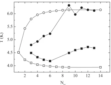
FIG. 4. The transition width for the samples MBnvs number of bilayersNbi. Experiment : shown are the temperatures for 0.9Rn (closed circles) and 0.1Rn(closed squares), withRnthe normalized resistance. Theory: open squares (circles) correspond to the maximum (zero) node state.
The curves in fixed field show a shift, but theR(T) behavior is essentially unchanged from the zero-field behavior, with multiple steps visible. The curves at fixed temperature behave differently and sharpen up appreciably in higher applied fields, from about 1 T to less than 0.2 T.
IV. THEORETICAL FRAMEWORK A. Formulation of the model
In order to explain these observations, a model was developed to calculate Tc of the different order parameter
configurations in finite multilayers. The onset of the critical state, in the diffusive limit and neglecting paramagnetic and spin-orbit effects, is described by a system of linearized Usadel equations1,18for the S and F layers (takingk
B=h¯ = 1): −π TcSξS2Fn(z)+ |ωn|Fn(z)=π T λ
ωm|ωD
Fm(z), (1)
−π TcS(ξF∗)2Fn(z)+[|ωn| +iEexsgn(ωn)]Fn(z)=0. (2)
Here,TcSis the bulk critical temperature of the superconductor,
ωn=π T(2n+1) are the Matsubara frequencies [n=0, ±1, . . . ,nD(T)], withnD(T) the integer part of the expression
(ωD/2π T −0.5) and ωD the Debye frequency, λ is the
effective electron-electron interaction constant,Fn(z) are the
Usadel anomalous Green functions, andEexis the exchange field energy. Thezaxis is taken perpendicular to the layers, while thexyplane atz=0 coincides with the mirror plane of the sample. Furthermore,ξS,ξF∗ are the dirty limit coherence
lengths in the S(F) metal, given by DS,F/(2π Tcs), with
DS,F the diffusion coefficients in S(F). These equations are
supplemented by matching and boundary conditions:19
ρ−1(zi+)Fn(z+i )=ρ−1(z−i )Fn(z−i ), (3)
Fn(z+i )=Fn(z−i )+γbξS
ρF
ρ(z−i )F
n(z−i ), (4)
V. N. KUSHNIRet al. PHYSICAL REVIEW B84, 214512 (2011)
FIG. 5. (Color online) Field dependence of the resistive transition of sample MA9. (a) ResistanceRas function of in-plane applied field
Ha at temperatures (left to right)T =4.25, 4.14, 4.05, 3.94, 3.82, 3.68, 3.54, 3.36, 3.25, 3.10, 2.94, 2.87, 2.74, 2.63, 2.51, 2.24, 2.13, 1.99, and 1.96 K. (b)R(T) for fields (right to left)Ha =0, 0.4, 0.5, 0.6, 0.7, 0.8, 0.9, 1.0, and 1.1 T.
Here L is the overall thickness of the multilayer, zi (i=
1,2, . . . ,2Nbi) are the zcoordinates of the interfaces,z±i ≡
zi±0, and ρ(z)=ρF,S for z in F, S, with ρF,S the
low-temperature specific resistance of the F, S layer. The parameter γb is defined as (2 F)/(3tbξF∗), with F the electron mean
free path in the ferromagnet and 0< tb <∞the transparency
parameter. For solving the set of equations the matrix method is used.20 The details of the calculations are described in AppendixB. With this model, values forTccan be calculated
for each order parameter configuration, since these are the eigenvalues of the matrix equations. The number ofTcvalues
is obviously given byNbi. They will be calledT(k), whereT(0)
denotes the configuration with zero nodes (the first symmetric solution), andT(Nbi−1)the configuration withN
bi−1 nodes.
B. An example: The five-bilayer system
To demonstrate the applicability of our approach, and in order to make the main features of the studied multilayers more transparent, we start with the examination of the sim-plest generic F/[5(S/F)] structure, an asymmetric multilayer consisting of five bilayers and a closing F layer. It contains
FIG. 6. (Color online) Eigenvalues of the critical temperatureT(k)
of the F/[5(S/F)] structure as a function of F layer thicknessdF, calculated for dS=4.67ξS. Also shown are the solutions for the infinite multilayerTc0andTcπ.
the smallest amount of blocks necessary to demonstrate the effects we have observed experimentally in more complex systems. We need materials constants for the calculation, and we have chosen them close to ones of Nb/PdNi bilayers9; namely, ρS/ρF =0.29, γbξF∗/ξF =0.28, and ξF =0.5ξS,
where ξF ≡ √
DF/Eex is the characteristic decay length of
the order parameter. We also take the thickness of the S layer large enough (dS=4.7ξS) in order to satisfy the conditions
of the single mode approximation.21 Figure 6 shows the thickness dependence of eigenvaluesT(k)(d
F) for five-bilayer
system. Also shown are the results for the infinite multilayer calculation, with the symmetric solutionTc0(solid gray line)
and the antisymmetric solutionTcπ (dashed gray line). The
eigenvalues T(k) are numbered according to the number of zeros of appropriate eigenvector functions (k)(z) (see AppendixBfor details).
It is clearly seen that there is an intersection of all the curves T(k)(d
F) (k=0, . . . ,4), which occurs in a narrow
regions in the vicinity of 0–π crossoverdF∗ ≈1.35ξF. In the
intervaldF < dF∗ the hierarchy inT(
k)isT(k+1)< T(k), while
for dF > dF∗ this is changed to the opposite T(k+1)> T(k).
For dF < dF∗, the zero-node state occurs, as described by
eigenvector function (0)(z) shown in Fig. 7(a). Above d∗
F
the system goes into the four-node state, which is basically aπ state, and described by the eigenvector function (4)(z) [Fig.7(b)].
Now let us focus on the immediate proximity to the point of 0–π crossover and understand the evolution the order parameter is going through. Figure 8 shows the detailed variation ofT(k) around the crossing point at dF∗. Looking closely, all curves evolve in a nonmonotonous fashion. The solutionsT(0,1)show a jump down, the solutionsT(3,4)show
a jump up, andT(2) shows a kink atd∗
F. However, there is
continuity in the variation of the eigenvalues in the sense that at the degeneracy point the variation inT(0)is continued
FIG. 7. Real+(z) and imaginary [−i−(z)] parts of eigenvector functions (a) (0)(z) and (b) (4)(z) calculated for d
F =0.7ξF≈ 0.52dF∗anddF =2.2ξF≈1.63dF∗, respectively.
T(1), and T(4) in T(0). The evolution of the eigenfunctions reflect this change in the sense that, in the vicinity of the degeneracy point, they start to take on the shape of the continuation.
For instance, the eigenfunction(0)(z) transform from the shape atdF= 0.7ξFgiven in Fig.7(a)to the one atdF =1.33ξF
(very close to the degeneracy point) shown in Fig.9(a). The similarity to a two-node function is becoming apparent, which is the way in which the eigenvalue continues. Similarly, the eigenvalue with the proper function(4)(z) is a continuation
of the one with(2)(z) and atdF =1.37ξF (just beyond the
degeneracy point)(4)(z) still shows strong resemblance to a two-node function as can be seen in Fig.9(c).
Figure 9 is also meant to make another point; namely, how the ground state of the system, casu quo the highest eigenvalue (which isTc) evolves arounddF∗. Figures9(a)–9(c)
present those eigenfunctions which in turn determineTcwhen
increasing dF from 1.33ξF up to 1.37ξF; namely, (0)(z),
(1)(z), and(4)(z). An interesting feature of the crossover
FIG. 8. (Color online) Eigenvalues of critical temperatureT(k)of
F/[5(S/F)] structure as a function of F layer thickness in immediate proximity to the point of 0–πcrossover (see Fig.6).
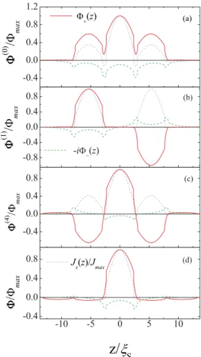
FIG. 9. (Color online) Real+(z) and imaginary [−i−(z)] parts of eigenvector functions and supercurrent densityJx(z) calculated for the F/[5(S/F)] multilayer for (a)dF =1.33ξF, (b) and (d)dF = 1.35ξF, and (c)dF =1.37ξF.
is that upon approachingdF∗, superconductivity is practically suppressed in the outward layers, while exactly at the crossover it disappears in the central layer. However, this solution is only marginally lower in energy than the solution emerging from (0,2,4)(z) given in Fig. 9(d). Another interesting feature is
the behavior of the spatial distribution of the supercurrent density Jx(z), which shows weak countercurrents flowing
along the central ferromagnetic layers [see Fig.9(a)]. It means that a measurement current will actually be accompanied by countercurrents.
C. Engineering an order parameter
V. N. KUSHNIRet al. PHYSICAL REVIEW B84, 214512 (2011)
FIG. 10. (Color online) Eigenvector functions and supercurrent densityJx(z) calculated for the F/[5(S/F)] multilayer with (a) enlarged thickness of the two central F layers and (b) with reduced thickness of the central S layer.
determines the multilayer critical temperature. Our numerical calculations confirm this statement. Figure10gives the spatial distribution of the eigenfunctions calculated for two particular structures of the F/[5(S/F)] model system, which has a central S layer. In the first case [Fig.10(a)], the thicknesses of the F layers directly contacting the central S layer aredF =2.2ξF,
while the other F layers have dF =ξF. In the second case
[Fig.10(b)], the central S layer thicknessdS=2ξS, while the
other S layers havedS=4.67ξS. In the first case, the ground
state becomes(2)(z), while in the second it is(1)(z). It is
important to note that also in these configurations (as also shown in Fig. 10) the application of a measuring current into the structure will be accompanied by generation of countercurrents.
Obviously, in the presence of structural inhomogeneities in any true structure consisting ofNbi (F/S) bilayers, it will be energetically favorable for the countercurrents to be closed by forming current loops having the smallest characteristic dimension. It means that such a multilayer is unstable against the formation of clusters of current loops in the transition from the normal to the superconducting state. Moreover, for the set of parameters under which a multilayer is close to the 0 toπ transition such current loops (stretching over varying numbers of bilayer blocks) should, in the transition, leave fingerprints of the otherwise hidden eigenvaluesT(k)of smaller blocks within
the full structure. This we believe to be is what we essentially observe.
V. ANALYSIS AND DISCUSSION
We use the theoretical model developed above to study quantitatively the variation of Tc as found in the series
MBn as well as in the stepped structure in MA9. The parameters to be chosen and varied are the usual ones for proximity effect problems. Fixed areTcS =9.2 K (the bulk
value for Nb) and ωD=275 K. Fitting parameters then in
principle are the proximity parameterγ =ρSξS/(ρFξF) and
the transparency parametertb. However, the fitting strategy is
not straightforward for the multilayers, since it is not simply Tcwhich is to be fitted. We therefore use a slightly different
approach, and determine the necessary parameters using the basic multilayer building blocks MS1 and MS2, which do have a well-determined Tc and a transition width of 50 mK. We
optimize the following parameters around the values found in Ref. 9: ξS=5.6 nm (5.6 nm), ξF∗ =5.0 nm (6.2 nm),
p=ρS/ρF =0.15 (0.26), and γb=0.22 (0.13), where the
values in brackets are the ones used in Ref.9. The current parameter set is quite close to the previous one, which gives confidence in the procedure. We then use these parameters to calculate the setsTnfor the series MBn. The values for the
T(0)≈T
c0(no nodes) andT(8)≈Tcπ(largest number of nodes)
are given in Fig.4.
The first striking conclusion is that the transition widths for largeNbiare roughly given by the spread ofT(k). In particular,
the upper limit is very well reproduced by the zero-node solutions (open circles in Fig. 4). The lower limit (open squares) is the maximum nodal state. The critical temperature for the lower limit is always less than the measured values, for reasons to be discussed below. Also clear is that below Nbi=5, the transition singles out only one mode. Before
discussing the behavior of these samples in more detail, we turn to the multistep transition of sample MA9, shown in Fig.3 and enlarged in Fig.11. The typical behavior of our
FIG. 11. Normalized resistive transition for sample MA9. Ver-tical lines mark the positions of allT(k)values as calculated using
sample we examined whether all nineT(k)s can be reasonably
fitted in the transition. This turns out to work surprisingly well. Using ξS=5.2 nm (5.6 nm), ξF∗ =5.2 nm (5.0 nm),
p=ρS/ρF =0.10 (0.15), and γb=0.16 (0.22) (with the
values in parentheses now the ones used in fitting the MBn series), we findT(k) values as plotted in Fig.11. We do not
claim that we literally observe theseT(k)s. The point is rather
that this sample spans the full transition width of about 2.5 K allowed by its physical parameters, which means that for MA9 the transition to superconductivity starts with the 0-node state and ends with the maximum nodal configuration.
The unequivocal message from the experiments is that our large-Nbi multilayers have transition widths which are
connected to the different possible order parameter configura-tions, starting with the 0-node symmetric one. Still, it isnot
as if the system sequentially samples them; in that case the highest of the possibleTcs in the system would determine the
transition temperature. The picture is a bit more subtle, and for the discussion we refer to a recent study we performed on the transition width in simple S/F/S trilayers made with Nb and Cu41Ni59, where dF was varied through the 0–π
transition region.10 In that region, similar broadenings were found as in the multilayers under discussion, although the values ofTc were significantly less, not more than 0.5 K.
For the trilayers we proposed a model in which, under the influence of small variations in thickness, interface roughness, and exchange energies, the system in the transition actually has to be viewed as a network of S-N-S and S-F-S junctions. At the onset of superconductivity, superconducting islands start to form in the S layers, separated by still normal regions in the same layer, while the islands are also connected to islands in other layers through the weak F material. Local loops between two S layers (1 and 2) may now emerge of type S1-N1-S1-F-S2-N2-S2-F-S1, containing two S-F-S junctions.
If one of these goes into aπ state, the loop can maintain a circulating Josephson current which works against the growth of the S islands and broadens the transition. Of course, once the S islands coalesce, the circulating currents disappear and the system is in a well-defined state with respect to the phases. Obviously a similar mechanism should be at work in our multilayers, where the F-layer thickness is in the region of allowing π states. But now the multilayer allows a larger variety of networks to be formed on the basis of order parameter configurations with numbers of nodes up toNbi−1.
The picture which then emerges is that the first networks which occur below the onset of superconductivity are like 0-node configurations. Going down in the transition, loops between two adjacent S layers survive longest, which is like the full-nodal configuration, although this configuration is not necessarily reached. For that, the structure should have the correct periodical structure, and if that condition is not fulfilled, the system separates in different subblocks having a smaller number of nodes and a higher Tc. In our case the F-layer
thickness is not optimal, and we usually findTcfor the system
above that was predicted by the full nodal solution. It is worth noting that a similar model of Josephson networks with 0 and πcontacts was considered almost 20 years ago in connection with the paramagnetic Meissner effect (“Wohlleben effect”)
FIG. 12. (Color online) Resistance R vs temperature T for two different sets of multilayers consisting of building blocks Cu0.41Ni0.59(3 nm)/Nb(30 nm), and in different applied magnetic
fields; from right to left: (0, 0.25, 0.5, 0.75, 1) T. (a) is an asymmetric set of type F/[9(S/F)]; (b) is a symmetric set where the outer F layers have half the thickness of the inner ones.
in high-Tc ceramics.23–26 The main difference with our work
is that the finite S/F multilayer can spontaneously divide into fragments with differentTcs.
The measurements of the field dependence of the transition performed on sample MA9 [see Fig. 5(a)] are in line with this picture. The variation of the widths of the transition as a function of applied Ha are given in the inset of Fig. 11.
They show that for decreasing temperature,Tccontinuously
V. N. KUSHNIRet al. PHYSICAL REVIEW B84, 214512 (2011) Finally, to show the generality of our results, we prepared
a multilayer set on the basis of the weak ferromagnet Cu0.41Ni0.59(called CuNi), also used in earlier experiments.27
The asymmetric sample consisted of nine blocks CuNi(3 nm)/ Nb(30 nm), with a closing layer of CuNi(3 nm) cov-ered by Nb(2 nm) to prevent oxidation. The symmet-ric sample had outer layers of 1.5 nm CuNi. The re-sults in Fig. 12 sketch exactly the same picture as for the multilayers with PdNi. The thickness of the CuNi layer is close to the transition to the π state, and the asymmetric sample has a transition width of about 0.5 K, which sharpens to 0.2 K in a field of 1 T. The symmetric sample shows transition widths of less then 0.1 K. The smaller widths in the asymmetric case compared to the PdNi samples is probably due to the somewhat larger thickness of the Nb layers, which result in a Tc around 7.5 K. In conclusion,
we have worked out the concept of different possible order parameter configurations in S/F multilayers. We have used this in analyzing the increasing transition width in S/F multilayers in terms of simultaneously emerging superconducting islands and Josephson junction networks, and we have shown that this width can actually be quantitatively predicted on the basis of the possible Tcs of the system as given by the different
configurations. We also showed how the model we developed allows us to engineer different order parameter configurations. It would seem that this property of S/F multilayers could lead to novel devices if they can be brought to switch between different configurations, in particular between zero, one, and two nodes. This will be an area of future research.
ACKNOWLEDGMENTS
The work has been partially supported by RFBR-BFBR Grants No. 12-02-90010 (M.Yu.K.) and No. F10R-063 (V.N.K. and S.L.P.), by the Italian MIUR-PRIN 2007 project “Propriet`a di trasporto elettrico dc e ac di strutture ibride stratificate su-perconduttore/ferromagnete realizzate con materiali tradizion-ali”(C.C. and C.A.), by the CNR within the CNR Short Term Mobility Program (C.C.), and by the “Stichting voor Fundamenteel Onderzoek der Materie (FOM)” (J.A.). J.M. v.d Knaap is acknowledged for the preparation of the Nb/CuNi multilayers. The research leading to these results and the final preparation of the manuscript has received funding from FP7/2007-2013 under Grant No. 264098-MAMA. Support from the ESF-programme “Nanoscience and Engineering in Superconductivity” (NES) is also acknowledged.
APPENDIX A:dFAT THE 0–πTRANSITION
Generally, many factors (among which, e.g., the trans-parency of the interfaces and the strength of the magnetic scattering) determine the thickness dF,cr at which an S/F
multilayer crosses over from the 0 state to the π state, and it is not possible to give a simple estimate in terms of what is actually a complex coherence lengthξF1+iξF2,
where ξF1 sets the decay length andξF2 sets the oscillation
length of the order parameter. We neglect magnetic scattering, as we did above, so that both lengths are given by ξF
(and the oscillation wavelength by λF =2π ξF). Under that
assumption, an estimate can be given for some simple cases.
In the case of an S/F bilayer, Fominovet al.21find for a fully transparent interface that 4dF,cr/λF ≈0.7, which means the
ratiodF,cr/ξF =0.35π =1.1. It was argued in Ref. 21 that
this result can be qualitatively understood in terms of a simple interference picture which yields dF,cr/ξF =(π/4)≈1.55,
which still overestimates the actual value by about 40%. If the interface is less than fully transparent, the ratio goes down, but also the minimum inTc(dF) disappears. For the case of the
infinite S/F multilayer with fully transparent interfaces, the calculations by Radovicet al. yielded dF,cr/ξF ≈1,8 while
Buzdin1 finds the first 0–π transition to occur atd
F,cr/ξF ≈
1.18. Again, when the interface transparency decreases, the ratio goes down. Note that for the case of the asymmetric five-layer system above, we finddF,cr/ξF ≈1.35, still quite
close to the (symmetric) infinite multilayer case.
Next to the minimum inTc, also the minimum in the critical
currentIc,min, can be used to find the crossover. NearTc this
minimum is found at the samedF,cr as for theTc minimum;
namely at 1.18ξF,1 and at somewhat lower value for lower
temperatures. Also here, the introduction of insulating (I) barriers, leading to SIFS or SIFIS configurations, can strongly lower the value of the crossover thickness.1,28 The bottom line is that in general, the crossover value depends on many parameters, with few simple rules.
Experimentally, values forξF in Pd1−xNix are as follows.
For x =0.12, Khaire et al. find an oscillation length ξF2
of 4.4 nm from the critical current in S/F/S junctions with relatively clean layers. Baladi´e and Buzdin findξF =3.0 nm
by reanalyzing the data of Kontos et al.29,30 in the correct SIFS junction geometry. For x =0.14, Cirillo et al. found ξF =3.4 nm from aTcanalysis of S/F bilayers,31and Matsuda
et al. found ξF =3.5 nm, also from the Tc of bilayers.32
Forx=0.19, the value of the present samples, Cirilloet al.
found aTcminimum around 3.0 nm in bilayers. Neglecting
magnetic scattering, and noting that the interface transparency in these bilayers is rather high, this yielded a value ofξF =
2.8 nm9; similarly, a T
c study of SFS trilayers also yielded
ξF =2.8 nm.33Note the more or less monotonic decrease of
ξF with increasing Ni concentration. For a symmetric infinite
multilayer with highly transparent interfaces, the crossover can therefore be expected somewhat below the full transparency value of 1.2ξF =3.4 nm. We estimate the transparency effect
to yield 3.1 nm. The thickness used in the experiment is a little bit lower than that, but this does not appear to be critical.
APPENDIX B: THEORETICAL DETAILS
It is convenient to write the solution of boundary problem (1)–(5) in the matrix form20
Y(z)=Rˆ(z)Y(−L/2), (B1)
where Y(z) is the direct sum +(z)⊕+(z)⊕−(z)⊕ −(z), where ±(z)=(±,0±,1· · ·±,nD+1)
tr are (n
D+
1)-dimensional vector functions (by the symbol tr we denote here the transposition operation) related to Fn by ±,n =
(Fn±F−n−1)/2, and ˆR(z) is the matrizant of the system
ˆ
R24,13(L/2)(−L/2)=0. (B2)
Here=+⊕−is a column vector, while
ˆ
R24,13 =
ˆ
R2,1Rˆ2,3
ˆ
R4,1Rˆ4,3
, (B3)
where ˆRα,β(α,β=1,2,3,4) are (nD+1)×(nD+1) matrix
blocks of matrix ˆR.
The condition of existence of nontrivial solutions of the system (B2) gives the characteristic equation in the form
det[ ˆR24,13(L/2)]=0. (B4)
The matrizant ˆRin Eq. (B4) can be found in explicit form and is expressed in terms of the product of the matrizants of S-( ˆS) and F-( ˆM) layers and the matrices ˆSF, ˆF S determined by
the matching conditions (3), (4). In particular for the structures F/Nbl(S/F) the matrizant, which is connected vectorsY(−L/2)
andY(L/2), has the form
ˆ
R(L/2)=Mˆ(dF)[ ˆF SSˆ(dS) ˆSFMˆ(dF)]Nbl. (B5)
Matrices ˆS, ˆM, and ˆSF(F S)can be written as
ˆ
S(z)=
ˆ
CSˆ+(z) ˆCtr 0ˆ
ˆ
0 Sˆ−(z)
(B6)
and matrices ˆS+(z) and ˆS−(z) in (B6) are given by
ˆ
S±(z)=
diag[cosh(k±nz)] diag[(kn±)−1sinh(kn±z)] diag[kn±sinh(kn±z)] diag[cosh(k±nz)]
.
(B7)
Here diag[an] is diagonal matrix with the main
diago-nal elements a0,a1, . . . ,anD; kn+=ξS−1 √
−2T μn/TcS, kn−=
ξS−1√(2n+1)T /TcS, whereμn≡μn(T) are the roots of the
equation
ψ
ωD
2π T +μ+1
−ψ
1 2+μ
= ψ
ωD
2π TcS +
1 −ψ 1 2 , (B8)
whereψ(t) is the digamma function. The matrix ˆCin (B6) has the form
ˆ C=
ˆ
C 0ˆ
ˆ
0 Cˆ
,
where ˆCis an orthogonal matrix, which is intended by vectors
cnm=
2sm
2n+1+2μm
, (B9)
containing the normalized coefficients
sm= nD
l=0
4 (2l+1+2μm)2
−1/2
. (B10)
ˆ
M(z)= Re[ ˆm(z)] ıIm[ ˆm(z)]
ıIm[ ˆm(z)] Re[ ˆm(z)] , (B11)
where
ˆ
m(z)=
diag[cosh(κnz)] diag[(κn)−1sinh(κnz)]
diag[κnsinh(κnz)] diag[cosh(κnz)]
,
(B12)
and the characteristic lengthsκnare given by the following
formula:
κn=
1 ξF∗
ıEex+ωn
π TcS
. (B13)
Finally, from (3) and (4) it follows:
ˆ
F S(SF) =
ˆ
PF S(SF) 0ˆ
ˆ
0 PF Sˆ (SF)
, (B14)
where
ˆ
PF S=
ˆ
1 γbξF∗p−11ˆ
ˆ
0 p−11ˆ
, PSFˆ =
ˆ
1 γbξF∗1ˆ
ˆ
0 p1ˆ=.
(B15)
In (B15) the parameter p is the ratio of normal resistivities ρS/ρF, and the unit and zero matrices have (nD+1)
dimen-sionality.
Thereby, the equations (B1)–(B15) determine the full solution of the boundary problem (1)–(5). From the char-acteristic equation (B4) and from Eq. (B2) one can get the T(k) eigenvalue set and the corresponding eigenvectors (k)(−L/2), respectively. After that, making use of (B1),
it is possible to find the eigenvector functions (k)(z). The
largest eigenvalue from theT(k) eigenvalue set is the critical
temperatureTcof multilayer structure.
In an experiment, to get information aboutTc, it is necessary
to apply a measurement (transport) currentJx in the direction
parallel to the S-F boundary planes,for example, along the OX axis. To find out the spatial distribution of this current in the direction perpendicular to the S-F interfaces direction (OZ) we should take into account that this current is small. In first approximation we can then neglect the suppression of the ± functions by this current and need not take into consideration the items in Eqs. (1) and (2) which are responsible for this depairing effect. We can further suppose that the existence ofJxcan be described by introducing factors
exp(ikx) independent ofωin all±functions with the wave vectorkis proportional to the condensate superfluid velocity. Substitution of that form of solution into an expression for the supercurrent density1,34,35
J= 4π T
ieρ(z)(+
∗tr∇
+−−∗tr∇−−c.c.), (B16)
results inJx(z) in the form
Jx(z)=
8kπ T eρ(z)(+
∗tr
+−−∗tr−). (B17)
V. N. KUSHNIRet al. PHYSICAL REVIEW B84, 214512 (2011) can conclude that for everyT(k)there is a well-defined spatial
current distributionJ(k)
x (z). It is necessary to mention that the
existence of−(z) component in (B17) under certain condi-tions may lead to an alternation of sign ofJx(z) with change of
coordinatez, that is to generation of countercurrents in the S-F multilayer structures. This effect is the consequence of the ex-istence of exchange interactions in F layers. In S-N multilayers −(z) is identically zero and these countercurrents do not exist.
1A. I. Buzdin,Rev. Mod. Phys.77, 935 (2005).
2V. A. Oboznov, V. V. Bol‘ginov, A. K. Feofanov, V. V. Ryazanov,
and A. I. Buzdin,Phys. Rev. Lett.96, 197003 (2006).
3A. Bauer, J. Bentner, M. Aprili, M. L. Della-Rocca, M. Reinwald,
W. Wegscheider, and C. Strunk,Phys. Rev. Lett.92, 217001 (2004).
4I. A. Garifullin,J. Magn. Magn. Mater.240, 571 (2002).
5P. H. Barsic, O. T. Valls, and K. Halterman,Phys. Rev. B75, 104502
(2007).
6S. Takahashi and M. Tachiki,Phys. Rev. B33, 4620 (1986). 7A. I. Buzdin and M. Yu Kupriyanov, Pisma Zh. Eksp. Teor. Fiz.52,
1089 (1990) [JETP Lett.52, 487 (1990)].
8Z. Radovi´c, M. Ledvij, L. Dobrosavljevi´c-Gruji´c, A. I. Buzdin, and
J. R. Clem,Phys. Rev. B44, 759 (1991).
9C. Cirillo, A. Rusanov, C. Bell, and J. Aarts,Phys. Rev. B 75,
174510 (2007).
10S. L. Prischepa, C. Cirillo, C. Bell, V. N. Kushnir, J. Aarts,
C. Attanasio, and M. Yu. Kupriyanov,Pis’ma Zh. Eksp. Teor. Fiz.
88, 431 (2008)[JETP Lett.88, 375 (2008)].
11L. G. Parrat,Phys. Rev.95, 359 (1954).
12L. Nevot and P. Croce,Rev. Phys. Appl.15, 761 (1980). 13A. P. Payne and B. M. Clemens,Phys. Rev. B47, 2289 (1993). 14C. L. Chien, J. S. Jiang, J. Q. Xiao, D. Davidovic, and D. H. Reich,
J. Appl. Phys.81, 5358 (1997).
15Y. Obi, M. Ikebe, and H. Fujishiro,Phys. Rev. Lett. 94, 057008
(2005).
16W.-C. Chiang, J. G. Lin, K. H. Hsu, D. S. Hussey, and D. V. Baxter,
J. Magn. Magn. Mater.304, E97 (2006).
17V. Shelukhin, A. Tsukernik, M. Karpovski, Y. Blum, K. B. Efetov,
A. F. Volkov, T. Champel, M. Eschrig, T. L¨ofwander, G. Sch¨on, and A. Palevski,Phys. Rev. B73, 174506 (2006).
18K. D. Usadel,Phys. Rev. Lett.25, 507 (1970).
19M. Y. Kuprianov and V. F. Lukichev, Zh. Eksp. Teor. Phys.94, 139
(1988) [Sov. Phys. JETP67, 1163 (1988)].
20V. N. Kushnir and M. Yu. Kupriyanov, Pis’ma v Zh. Eksp. Teor.
Fiz.93, 597 (2011).
21Ya. V. Fominov, N. M. Chtchelkatchev, and A. A. Golubov,Phys.
Rev. B66, 014507 (2002).
22A. Buzdin and A. E. Koshelev,Phys. Rev. B67, 220504 (2003). 23W. Braunisch, N. Knauf, V. Kataev, S. Neuhausen, A. Gr¨utz,
A. Kock, B. Roden, D. Khomskii, and D. Wohlleben,Phys. Rev. Lett.68, 1908 (1992).
24F. V. Kusmartsev,Phys. Rev. Lett.69, 2268 (1992).
25S. V. Panyukov and A. D. Zaikin,Physica B203, 527 (1994). 26D. Khomskii,J. Low Temp. Phys.95, 205 (1994).
27M. Flokstra and J. Aarts,Phys. Rev. B80, 144513 (2009). 28A. S. Vasenko, A. A. Golubov, M. Yu. Kupriyanov, and M. Weides,
Phys. Rev. B77, 134507 (2008).
29A. Buzdin and I. Baladi´e,Phys. Rev. B67, 184519 (2003). 30T. Kontos, M. Aprili, J. Lesueur, F. Genet, B. Stephanidis, and
R. Boursier,Phys. Rev. Lett.89, 137007 (2002).
31C. Cirillo, S. L. Prischepa, M. Salvato, C. Attanasio, M. Hesselberth,
and J. Aarts,Phys. Rev. B72, 144511 (2005).
32K. Matsuda, H. Niwa, Y. Akimoto, T. Uemura, and M. Yamamoto,
IEEE Trans. Appl. Supercond.17, 3529 (2007).
33V. N. Kushnir, S. L. Prischepa, J. Aarts, C. Bell, C. Cirillo, and
C. Attanasio,Eur. Phys. J. B80, 445 (2011).
34A. A. Golubov, M. Yu. Kupriyanov, and E. Il’ichev,Rev. Mod.
Phys.76, 411 (2004).
35F. S. Bergeret, A. F. Volkov, and K. B. Efetov,Rev. Mod. Phys.77,

![FIG. 6. (Color online) Eigenvalues of the critical temperature T (k) of the F/[5(S/F)] structure as a function of F layer thickness d F , calculated for d S = 4.67ξ S](https://thumb-us.123doks.com/thumbv2/123dok_us/8271416.2190798/4.911.102.413.101.616/online-eigenvalues-critical-temperature-structure-function-thickness-calculated.webp)
![FIG. 10. (Color online) Eigenvector functions and supercurrent density J x (z) calculated for the F/[5(S/F)] multilayer with (a) enlarged thickness of the two central F layers and (b) with reduced thickness of the central S layer.](https://thumb-us.123doks.com/thumbv2/123dok_us/8271416.2190798/6.911.106.415.99.567/eigenvector-functions-supercurrent-calculated-multilayer-enlarged-thickness-thickness.webp)

