C-Cube Microsystems
PhyCDTM
PlavCDTM
CL480 MPEG System
Decoder User's Manual
C-Cube
ii C-Cube Microsystems
C-Cube Microsystems reserves the right to change any products described herein at any time and without notice. C-Cube Microsystems assumes no responsibility or liability arising from the use of the prod-ucts described herein, except as expressly agreed to in writing by C-Cube Microsystems. The use and purchase of this product does not convey a licence under any patent rights, copyrights, trademark rights, or any other intellectual property rights of C-Cube Microsystems. Trademark Acknowledgment:
PlayCD is a trademark of C-Cube Microsystems.
C-Cube and the corporate logo are registered trademarks of C-Cube Mi-crosystems.
© C-Cube Microsystems 1994 All rights reserved
C-Cube Microsystems 1778 McCarthy Boulevard
Milpitas, CA 95035 Telephone (408) 944-6300
Fax (408) 944-6314
Customer Comments and Feedback:
If you have any comments about this document, send them to the C-Cube Technical Publications Department at the address listed above, or send e-mail to:
Preface
This manual is the primary source of technical information for the op-eration and programming of the C-Cube CL480 MPEG System Decod-er.
This manual is intended for:
o System designers and managers who are evaluating the CL480 for possible use in a system.
o Design, software and system engineers developing a decoding system using the CL480 for whom a comprehensive programming background as well as a detailed understanding of MPEG com-pression is assumed.
In particular, . readers should understand the MPEG standard: Coded Representation of Picture, Audio and Multimedia/Hypermedia
Informa-tion, ISO 11172. This document is available from the American
Nation-al Strandards Institute (ANSI), 11 West 42nd St., New York, NY 10036, (212) 642-4900.
This manual is divided into three main sections:
o Section I, General Information, presents an introduction to the CL480 and the MPEG standard that it implements.
o Section II, Hardware, describes signals, operational information for the external interfaces of the CL480, registers, and detailed electrical and mechanical specifications.
Audience
Related
Publications
Organization
Conventions
iv C-Cube Microsystems
o Section III, Software, describes the CL480's microcode, and in-cludes an alphabetical listing of all macro commands available to the programmer. Note: the microcode information in this manual applies to CL480 version 2.0.
Please note the following notation examples and conventions used in this manual: Notation Examples Ox1c3 110112 IMEM
VIE, Res
IMEM[3] CPU_cntI[O] IMEM[0][15] IMEM[3][2:0]
Explanation
"Ox" prefix indicates a hexadecimal number. "2"subscript indicates a binary number.
Four-letter mnemonics indicate on-chip memories, starting with a letter to indi-cate function of memory, and ending with "MEM." For example, IMEM is the CL480's instruction memory.
This format indicates a register name. The first part of a register name is a group specifier, given in all upper-case. The second part (separated from the first by an underscore and given in alilower-casel is a register specifier, indi-cating the function performed by the register within the group. In the examples shown, CPU_cntl and CD_cntl are separate registers, even though both have the same register specifier, "cnt/."
Italicized acronyms or abbreviations (initial or all capsl indicate bit field names within registers or data words.
Square bracket notation similar to C language array subscripting indicates words within memories, and bits within words and registers. IMEM[3], for ex-ample, is the 16-bit word at address 3 within 1M EM, while CPU_cntl[O] is bit 0 of the CPU_cntl register. Similarly, IMEM[0][15] is the most significant bit of the word at IMEM address O.
Ranges of bits are indicated by numbers separated by a colon such as the three bits HMEM[3][2:0]. Ranges of words within a memory are indicated by numbers separated by a dash such as the eight words HMEM[O-7].
RESERVED or Indicates bit fields within registers which are not defined. RESERVED bit fields
Res may return any value when read and must be written with 0 (or 1 if so speci-fied). Writing the incorrect value to a RESERVED CL480 register bit will cause indeterminate behavior. In addition, all CL480 registers which are not explicitly given names are also RESERVED, and accessing these registers may cause in-determinate results on current or future CL480 implementations.
leftBorder Bold-face type represents macro command arguments.
return ( ) ; C-style syntax presented in courier typeface represents program pseudocode and equations.
Contents
Section
I. General Information1 Introduction
1.1 PlayCD Family 1-1
1.2 CL480 Features 1-2
1.2.1 Flexible Video Interface with High-Quality Video Output 1-2 1.2.2 Low Voltage, Low Power Operation in Small Package 1-3 1.2.3 Powerful, Easy-to-Use Microcode 1-3
1.3 Functional Description 1-4
1.3.1 Host Interface 1-5
1.3.2 CD Interface 1-5
1.3.3 DRAM/ROM Interface 1-5
1.3.4 Video Interface 1-5
1.3.5 Audio Interface 1-5
1.4 Consumer Electronics Application 1-6
2 MPEG Overview
2.1 MPEG Stream Structure 2.1.1 MPEG Stream Structure
2-2 2-2
vi C-Cube Microsystems
2.1.2 General Decoding Process 2.1.3 Video Stream Data Hierarchy 2.2 Inter-picture Coding
2.2.1 Picture Types
2.2.2 Video Stream Composition 2.2.3 Motion Compensation 2.3 Intra-picture (Transform) Coding 2.4 Synchronization
2.4.1 System Clock References 2.4.2 Presentation Time Stamps
Section II. Hardware
3 Signal Descriptions
3.1 Global Interface 3.2 Host Interface 3.3 CD Interface 3.4 DRAM Interface 3.5 Video Interface 3.6 Audio Interface 3.7 Programmable I/Os4 Host Interface Functional Description
4.1 Functional Overview4.2 Host Interface Registers
4.2.1 Host Interface Address Registers 4.2.2 Host Interface Data Registers 4.2.3 Accessing Host Interlace Registers 4.2.4 DRAM/ROM Access
4.2.5 Code FIFO Access 4.2.6 Internal Register Access 4.3 CL480 Read/write Operations
4.3.1 Host Write 4.3.2 Host Read
5 Local DRAM/ROM Interface
5.1 General Description 5-2
5.1.1 DRAM: Amount and Organization 5-2
5.1.2 ROM: Amount and Organization 5-3
5.2 DRAM Memory Bus Interface 5-3
5.2.1 DRAM Address Mapping 5-4
5.2.2 DRAM Interface Connections 5-4
5.3 ROM Memory Bus Interface and liming 5-5
5.3.1 DRAM_ROMTA Register 5-6
5.4 DRAM Memory Bus Timing 5-7
5.4.1 DRAM Page-Mode Read Timing 5-7
5.4.2 DRAM Page-Mode Write Timing 5-8
5.4.3 DRAM Refresh Timing 5-10
5.4.4 DRAM_REF Register 5-10
5.5 Memory Design Guidelines 5-11
6 CD Interface
6.1 General Description 6-1
6.1.1 Mode Functions 6-2
6.1.2 Mode Selection 6-2
6.2 Signal Interface 6-3
6.3 Disc and Signal Formats 6-4
6.3.1 CD Interface Input Signal Format 6-4
6.3.2 Compact Disc Sector Format 6-6
6.3.3 Data Alignmentfor CD-ROM 6-7
6.4 Design and Operation Considerations 6-8 6.4.1 Effects of Varying CD-DSP Speed 6-8
6.4.2 Maximum BCK Frequency 6-8
6.4.3 Maximum Rate for Error Correction 6-8 6.4.4 ROM Accesses during MPEG Decode and Display 6-8
7 Video Display Interface
7.1 Digital Video Standards 7.2 Video Display Unit 7.3 Timing Generation
7.3.1 (VSYNC or CSYNC)/HSYNCNCK Out 7.3.2 VSYNC/HSYNCNCK In
7.4 Video Operation and Design Guidelines 7.4.1 How to Set Video Output Mode 7.4.2 Aspect Ratio Limitations
7-2 7-3 7-3 7-5 7-5 7-6 7-6 7-6
7.4.3 CD-I Pixel Output 7-6 7.4.4 Transferring Video Data Via Host Bus 7-6 7.4.5 Vertical Interpolation and Full-Screen Playback Mode 7-6
8 Audio Interface
8.1 General Description 8-1
8.2 Signal Interface 8-2
8.2.1 Controling the Audio Output Level 8-2 8.2.2 Using Emphasis Flags to Identify the Data Stream 8-3
8.2.3 Low Power Operation 8-3
8.3 Clocking Modes 8-3
8.4 Operation and Design Guidelines 8-4
8.4.1 Audio Buffer Underflow 8-4
8.4.2 DA-XCK and Cycle Jitters 8-4
9 Electrical and Physical Specifications
9.1 Operating Conditions 9-1
9.1.1 Duty Cycle 9-2
9.1.2 Power Pin Supply Voltages 9-2
9.1.3 Power-up and Power-down Constraints 9-3
9.2 AC liming Characteristics 9-3
9.2.1 Host Bus Interface liming 9-5
9.2.2 DRAM/ROM Bus liming 9-6
9.2.3 CD Interface liming 9-11
9.2.4 Video Bus liming 9-14
9.2.5 Audio Bus Timing 9-18
9.3 Package Specifications 9-19
9.3.1 Pin List 9-22
9.3.2 Package Drawings 9-24
10 Registers
10.1 CL480 Register Categories 10-2
10.1.1 Direct-access Registers 10-3
10.1.2 Indirect-access Registers 10-4
10.2 Host Interface Register 10-5
10.3 Internal CPU Registers 10-6
10.3.1 CPU Execution Registers 10-6
10.3.2 IMEM Access Registers 10-6
10.4 CD Interface Registers 10-8
10.5 DRAM Interface Registers 10-10
10.6 Audio Interface Registers 10.7 Video Interface Register
Section III. Software 11 Microcode Overview
11.1 Process Configurations 11.1.1 Microcode-Load 11.1.2 Initialization 11.1.3 Command Process 11.1.4 Bitstream Input Process 11.1.5 Decode Process 11.1.6 Output Process 11.2 Error Handling 11.3 Interrupts 11.4 Starting Operation
11.5 Bitstream Buffer Under- 10verfiow 11.6 Programmable II0s
11.7 Fast-Forward and Fast-Reverse
12 Macro Commands
12.1 High Priority Commands 12.2 Low Priority Commands
12.2.1 Command FIFO 12.2.2 User Data FIFO 12.3 Writing Macro Commands 12.4 Macro Command Groups
12.4.1 Set-type Commands 12.4.2 Play-type Commands 12.4.3 Control Commands 12.5 Macro Command Reference
DisplayStill()
DisplayStill(startl, start2)
DisplayStill (start1, start2, stop1, stop2) DumpData() FlushBitstreamO Freeze() InquireBufferFullness() Pause() Play()
Play(start1, start2, stop1, stop2)
xC-Cube Microsystems
ResetO ScanO
SetBorderColorO SetErrorlevelO SetlnterruptMask() SetMuteO
SetStreamsO SetVideoFormatO SetWindowO SingleStepO SlowMotionO
A CL480 Design Guidelines
A.1 Choosing a Microcontroller and Crystal A.2 Initialization and ROM
A.3 Pull-up/Pull-down
12-23 12-24 12-25 12-26 12-27 12-29 12-30 12-31 12-32 12-33 12-34
1-1 Block Diagram of the CL480
1-2 CL480 in Consumer Electronics Configuration 2-1 General MPEG Decoding System
2-2 MPEG Data Hierarchy
2-3 Location of Luminance and Chrominance Values 2-4 Macroblock Composition
2-5 Forward Prediction 2-6 Bidirectional Prediction
2-7 Typical Display Order of Picture Types 2-8 Video Stream versus Display Ordering 2-9 Transform Coding Operations
2-10 SCR Flow in MPEG System 3-1 Bus Connection Diagram 3-2 Global Signals
3-3 Host Interface Signals 3-4 CD-Decoder Interface Signals 3-5 DRAM Interlace Signals 3-6 Video Interlace Signals 3-7 Audio Interlace Signals 4-1 CL480 Host Interlace
Figures
1-4 1-6 2-3 2-3 2-4 2-5 2-6 2-7 2-8 2-8 2-11 2-12 3-2 3-2 3-4 3-5 3-7 3-9 3-10 4-1
4-2 DRAM/ROM Address Formed by Host Address Registers 4-4 4-3 Sending Coded Data on CD Interface 4-5 4-4 Sending Coded data on Host Interface 4-5 4-5 C-FIFO Register Address Formed by A_MSB 4-6 4-6 Internal Register Address Formed by A_MSB 4-6 4-7 Host Interface local Register, Write Operation 4-8 4-8 Host Interface local Register, Read Operation 4-9
5-1 DRAM Interface 5-2
5-2 local DRAM/ROM Implementation with 256K x 16 DRAMs 5-5
5-3 ROM Access Timing 5-6
5-4 DRAM Page-Mode Read Timing 5-8
5-5 DRAM Page-Mode Write Timing 5-9
5-6 CAS-before-RAS Refresh Cycle 5-10
6-1 CD-Decoder Interface 6-1
6-2 System Block Diagram Showing Bypass of ROM Decoder 6-3
7-1 VCKversusHSYNC 7-4
7-2 VSYNC/HSYNCNCK Out Mode 7-5
7-3 VSYNC/HSYNCNCK In 7-5
8-1 Audio Interface Block Diagram 8-1
8-2 Audio Interface Clocking Modes 8-4
9-1 Host Interface local Register, Write Operation 9-5 9-2 Host Interface local Register, Read Operation 9-6
9-3 local DRAM Bus Timing 9-7
9-4 local DRAM CAS-before-RAS Refresh 9-8 9-5 CD Input Timing: 32-bit CD-BCK, Data latch Timing High 9-11 9-6 CD Input Timing: 32-bit CD-BCK, Data latch Timing low 9-11 9-7 CD Input Timing: 24-bit CD-BCK, Data latch Timing High 9-12 9-8 CD Input liming: 24-bit CD-BCK, Data latch liming Low 9-12 9-9 CD Input liming: 16-bit CD-BCK, Data latch Timing High 9-13
9-10 liming - VOE and VD 9-14
9-11 liming - VCK in at 27 MHz and VD (pixel data) 9-14
9-12 VSYNC Out versus HSYNC Out 9-15
9-13VSYNC In versus HSYNC In 9-15
9-14 VCK Out versus HSYNC Out 9-16
9-15 VCK In versus HSYNC In 9-16
9-16 VCK In versus HSYNC Out 9-16
9-17 VCK Out versus HSYNC In 9-17
9-18 VCK Out versus CSYNCNSYNC Out 9-17
9-19 VCK In versus CSYNCNSYNC Out 9-17
9-20 Audio Interface Timing Modes 9-18
9-21 Cl480 PQFP Pinout Diagram 9-20
9-22 Plastic Quad Flat Pack Physical Dimensions 9-24
10-1 IMEM Write Data Flow
10-2 Binary Representation of Conversion Coefficients 11-1 CL480 Microcode Process Configurations 11-2 CL480 Decoding Process Configuration 11-3 Mask Bit Allocation
10-7 10-17 11-2 11-3 11-8
Tables
4-1 Register Address Bits Used to Access DRAM, C-FIFO, and GBUS 4-2 4-2 Summary of Host Interface Local Registers 4-3
4-3 Memory Address Map 4-4
4-4 Internal Registers Decoded by A_MSB 4-7
5-1 DRAM Address Mapping 5-4
6-1 BCK/Data Rate/LRCK Comparison for the CD-Decoder 6-3 7-1 VD[23:0] Pin Assignments for RGB and YCbCr Data 7-3
8-1 Audio Interface Signals 8-2
8-2 Audio Attenuation Based on SetMute() or HOST_ENA=O 8-2 8-3 Relationship between XCK, BCK and LRCK for 44.1 KHz 8-4
9-1 Absolute Maximum Ratings 9-1
9-2 Operating Conditions 9-2
9-3 DC Characteristics 9-2
9-4 liming Characteristics - Local Register Write 9-5 9-5 liming Characteristics - Local Register Read 9-6 9-6 liming Characteristics - Local DRAM Bus 9-9
9-7 CD Input liming 9-13
9-8 liming Characteristics: VOE and VD 9-14 9-9 liming Characteristics: VCK and VD 9-14 9-10 liming Characteristics: VCK, HSYNC, and CSYNCNSYNC 9-17 9-11 liming Characteristics: VCK, HSYNC, and CSYNCNSYNC 9-18
xvi C-Cube Microsystems
9-12liming Characteristics: Audio 9-13 Host Bus Interface Pins 9-14 CD Interface Pins 9-15 Global Interface Pins
9-16 DRAM/ROM Bus Interface Pins 9-17 Audio Bus Interface Pins 9-18 Video Bus Interface Pins 9-19 Power and Miscellaneous Pins
9-20 Plastic Quad Flat Pack Physical Dimensions 10-1 CL480 Registers (listed by category) 10-2 Direct-access Registers
10-3 Indirect-access Registers 10-4 CD_cntl Register Bit Selection 10-5 CD_cnfg Register Bit Selection 10-6 DRAMjaddr Register IDs 10-7 Video Register IDs 11-1 Macro Command Summary 11-2 CL480 Interrupt Summary 12-1 Macro Command Summary 12-2 Mask Bit Assignments
12-3 Audio Attenuation Based on SetMuteO
Chapter 1
Introduction
1.1
The CL480 is an MPEG-l audio/video decoder and the first member of C-Cube's PlayCDTM family. Designed for consumer electronics prod-ucts and multimedia PCs, the CL480 reduces system cost by requiring only 4Mbits of DRAM, providing CD-ROM decoding, and providing a serial CD interface. The CL480 reduces development time and effort by performing system stream processing and audio/video synchronization. The CL480 provides high-quality output through its advanced video post-processing, sophisticated error concealment and support for high-resolution still pictures. The chip is particularly well suited for video CD players because it provides glueless interfaces to the CD-DSP, audio DAC and NTSCIPAL encoder.
PlayeD Family
The CL480 processes:
D CD-ROM data, CD-DA data, and constrained-parameters
MPEG-1 video bitstreams (typically SIF-resolution) in real time. D MPEG audio (Layer I or II) bitstreams.
The CL480 also features an extensive microcode set supplied with the hardware.
CL480 Features
1.2
CL480 Features
The CL480 has these key features:
o Integrates on one chip: MPEG audio and video decoding, video timing generation, and CD-ROM decoding functions
o Fully supports Video CD 2.0 and 1.1, Karaoke CD 1.0 and CD-I Green Bookl
o Accepts MPEG-l system streams or CD data streams with no ex-ternal parsing required
o Decodes and synchronizes SIF-resolution MPEG video and two channels of MPEG Layer 1 or 2 audio
o Resolutions include 352x240 at 30 Hz, 352x288 at 25 Hz, and 384x240 at 24 Hz
o Audio sample rates include 32, 44.1 and 48 kHz
o Decodes still images with coded resolutions up to 704x576 while decoding MPEG audio
o Requires only 4 Mbits of DRAM, even for PAL systems
o Accepts compressed data from 4-pin CD interface or from 8-bit host interface
o Glueless interfaces to CD-DSP, DRAM, ROM, audio DACs, and NTSCIP AL encoder
1.2.1 Flexible Video Interface with High-Quality Video Output
o Interpolates two different fields from each decoded frame to re-duce flicker and improve image quality on interlaced displays
o Performs frame-rate conversion so that display rate (typically 50 or 60 Hz) is independent of coded frame rate (typically 24, 25 or 30Hz)
o Performs horizontal interpolation of decoded video using a seven-tap filter
o Provides RGB or YCbCr video output using on-chip color space converter
o Supports HSYNC and VSYNC as inputs or outputs
1. The CL480 can implement CD-I but does not have all of the re-quired microcode. To work in the current type of CD-I systems, the CL480 requires a glue chip between its host interface and a 68000.
o Supports VCK input or generates VCK output by dividing GCK (40.5 MHz) by 3/2
o Optionally generates NTSC and PAL composite sync 1.2.2 Low Voltage, Low Power Operation in Small Package
o Operates with a supply voltage of 2.7 to 3.6 volts o Can accept 5-volt inputs
o Consumes less than 1 watt when decoding audio and video o Automatically divides GCK by 4t 8t or 16 to reduce power when
decoding MPEG audio only or when in CD-DA pass-through mode
o Packaged in a 128-pin small-outline PQFP (18mm x 18mm body) 1.2.3 Powerful, Easy-to-Use Microcode
o Performs audio/video synchronization
o Provides high-quality error concealment for bitstream errors o Performs error correction of CD-ROM data at 2.8 Mbps when not
decoding MPEG
o Supports low-cost systems with no host processor
o Can initialize itself from ROM connected to the DRAM interface o Provides high-level macro commandst allowing the host to
moni-tor and control the input, decode and output processes: o Play - Decodes and displays at normal rate
o SlowMotion - Decodes and displays at slower rate o SingleStep - Decodes and displays next picture o Scan - Decodes and displays next I-picture
o DisplayStill- Decodes and displays high-resolution still picture with audio
o Pause - Freezes display and decoding process o Freeze - Freezes display but continues decoding
o DumpData - Performs error correction on CD-ROM data o SetStreams - Selects which streams to decode
o SetWindow - Sets video window size and location o SetBorderColor - Sets border color
o SetErrorLevel - Sets error level for DisplayStill
CL480 Features
Functional Description
1.3
Functional Description
Host Data
...
Serial Bitstream 1 1
I·
1 1 1 1 1 1 1 1 1 1 1 1 1 ~ 1 1 1 1 1 1-o SetMute - Sets audi-o mute and attenuati-on
o SetVideoFormat - Sets format to NTSC, PAL or progressive o SetInterruptMask - Enables/disables interrupts to host o FlushBitstream - Discards contents of bitstream buffer o InquireBufferFullness - Measures data in bitstream buffers o Reset - Initializes the CL480 and its microcode
o Provides 13 interrupts, providing the host feedback on bitstream transition, display, and decoding processes
The CL480 decodes audio and video using a combination of hardwired coprocessors and a programmable RISC CPU, as shown in Figure 1-1. The coprocessors contain special-purpose logic to efficiently perform operations such as Huffman decoding. The RISC CPU is a general-pur-pose processor that controls the coprocessors and assists in the decoding process.
The microcode for the CPU is stored in DRAM and is loaded into on-chip memory as needed. During power-up, the microcode can either be loaded into DRAM by a host processor or can be read from a ROM con-nected to the CL480.
Host RISC Decompression
Interface CPU Coprocessors
1
Internal Bus1
1
t
..j Il
Video
1
Interface I ..
It 1
p Video Data
CD 1
DRAM/ROM 1
Interface
Interface 1
1 Audio
~ 1
j Interface 1 p Audio Data
1 1
- - - -
~---Figure 1-1
1-4 C-Cube Microsystems
DRAM and Optional ROM
[image:21.504.33.452.320.567.2]Each of the interface modules is described next. 1.3.1 Host Interface
The CL480's host interface is used to initialize the chip, supply com-pressed data, report status, and control operation. The CL480's host in-terface is based on an 8-bit bus tailored for low-cost applications; it minimizes pins while allowing the host to access DRAM, the code FIFO, and on-chip registers. These accesses are performed by writing the selected address to a series of three one-byte host address registers. Data is then read from or written to two one-byte data registers. 1.3.2 CD Interface
This interface is designed to receive serial compressed data from a CD-DSP. The CL480 supports six different input formats so that many of the popular CD-DSP chips can be used.
1.3.3 DRAMJROM Interface
The CL480's DRAMIROM interface provides a glueless interface be-tween the CL480 and external memory. It connects directly to fast page-mode DRAM, typically either one 256Kx16 DRAM or four 256Kx4 DRAMs. It can also be connected directly to an 8-bit ROM. The ROM access time can be programmed to be 3 to 34 GCKs. The ROM size re-quired for storing the CL480's MPEG microcode is less than 45 Kbytes. 1.3.4 Video Interface
The video interface performs horizontal and vertical interpolation of de-coded video. It accepts decompressed video data from the local DRAM and outputs it in:
o 24- or I5-bit RGB mode (formatted as BGR-BGR) o I6-bit YCbCr mode (formatted as CbY-CrY) o 8-bit YCbCr mode (formatted as Cb-Y -Cr-Y)
In YCbCr mode, pixels are output in 4:2:2 format, meaning luminance (Y) has twice the horizontal resolution of chrominance (Cb and Cr). 1.3.5 Audio Interface
The CL480 audio interface outputs decoded audio samples in bit-serial format and is able to control their attenuation. The CL480 also has a leftl right signal to indicate which channel is being output. The polarity of the leftlright signal and the order and number of bits per audio sample are programmable so that any of the popular audio DACs can be used.
Functional Description
Consumer Electronics Application
1.4
Consumer
Electronics
Application
The CL480 is designed for low-cost applications that include the con-sumer electronics market. In concon-sumer electronics products, such as the example shown in Figure 1-2, the CL480 typically receives a CD data stream from a CD-DSP chip via its 4-pin CD interface. This CD data stream could contain an MPEG-1 system stream, DA data or CD-ROM data.
Servo control
Host Front Function Panel Keys
Composite Video
Stereo Audio
p:::::::::=!
=
Additional components needed to make Video CD player from Audio CD playerFigure 1-2 CL480 in Consumer Electronics Configuration
Chapter 2
MPEG Overview
This chapter presents an overview of the Moving Picture Experts Group (MPEG) standard that is implemented by the CL480. The standard is of-ficially known as ISOIIEC Standard, Coded Representation of Picture, Audio and Multimedialhypermedia Information, ISO 11172. It is more
commonly referred to as the MPEG-l standard. 1
MPEG addresses the compression, decompression and synchronization of video and audio signals. The MPEG video algorithm can compress video signals to an average of about 112 to 1 bit per coded pixel. At a compressed data rate of 1.2 Mbits per second, a coded resolution of 352 x 240 at 30 Hz is often used, and the resulting video quality is compa-rable to VHS. Image quality can be significantly improved by using a more highly-compressed data rate (for example, 2 Mbits per second) without changing the coded resolution.
1. For documentation, contact the American National Standards Insti-tute (ANSI), 11 West 42nd St., New York, NY 10036, (212) 642-4900.
MPEG Stream Structure
2.1 MPEG Stream Structure
This section explains the structure of an MPEG system stream and in-troduces some concepts used in the rest of the chapter.
2.1.1 MPEG System Stream Structure
In its most general form, an MP EO system stream is made up of two lay-ers:
o The system layer contains timing and other information needed to demultiplex the audio and video streams and to synchronize audio and video during playback.
o The compression layer includes the audio and video streams.
2.1.2 General Decoding Process
Figure 2-1 shows a generalized decoding system for the audio and video streams.
The system decoder extracts the timing information from the MPEG system stream and sends it to the other system components. (Section 2.4, Synchronization, has more information about the use of timing in-formation for audio and video synchronization.) The system decoder also demultiplexes the video and audio streams from the system stream, and sends each to the appropriate decoder.
The video decoder decompresses the video stream as specified in Part 2 of the MPEG standard. (See Section 2.2, Inter-picture Coding, and Sec-tion 2.3, Intra-picture Coding, for more informaSec-tion about video com-pression.)
The audio decoder decompresses the audio stream as specified in Part 3 of the MPEG standard.
Video decompressed Decoder - . video
MPEG
System
system ---.. Decoder 1 - - - / stream
[image:26.505.51.443.312.531.2]Audio decompressed Decoder - . audio
Figure 2-1 General MPEG Decoding System
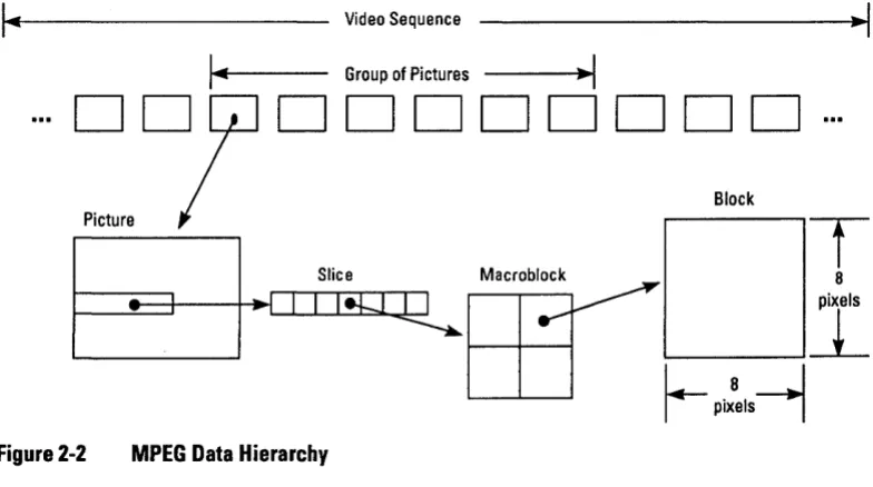
2.1.3 Video Stream Data Hierarchy
The MPEG standard defines a hierarchy of data structures in the video stream as shown schematically in Figure 2-2.
Video Sequence
Group of Pictures
~
I
MPEG Stream Structure
~I
...
~.D'
,---,e
1.
1DDDDDDDD
Block
T
8Slice Macroblock
II~~
pixels,---,l
r-
Pi:.I!--1
Figure 2-2 MPEG Data HierarchyMPEG Stream Structure
Video Sequence
Begins with a sequence header (may contain additional sequence head-ers), includes one or more groups of pictures, and ends with an end-of-sequence code.
Group of Pictures
A header and a series of one or more pictures intended to allow random access into the sequence.
Picture
The primary coding unit of a video sequence. A picture consists of three rectangular matrices representing luminance (Y) and two chrominance (Cb and Cr) values. The Y matrix has an even number of rows and col-umns. The Cb and Cr matrices are one-half the size of the Y matrix in each direction (horizontal and vertical).
Figure 2-3 shows the relative x-y locations of the luminance and chrom-inance components. Note that for every four lumchrom-inance values, there are two associated chrominance values: one Cb value and one Cr value. (The location of the Cb and Cr values is the same, so only one circle is shown in the figure.)
o
0
•
o
0
o
0
•
o
0
o
0
•
o
0
o
0
•
o
0
@) = Cb, Cr value
o
0
•
o
0
o
0
•
o
0
o
=YvalueFigure 2-3 Location of Luminance and Chrominance Values
Slice
One or more "contiguous" macroblocks. The order of the macroblocks within a slice is from left to right and top to bottom.
Slices are important in the handling of errors. If the bitstream contains an error, the decoder can skip to the start of the next slice. Having more slices in the bitstream allows better error concealment but uses bits that could otherwise be used to improve picture quality.
Macroblock
A 16-pixel by 16-line section of luminance components and the corre-sponding 8-pixel by 8-line section of the two chrominance components. See Figure 2-3 for the spatial location of luminance and chrominance components. A macroblock contains four Y blocks, one Cb block and one Cr block as shown in Figure 2-4. The numbers correspond to the or-dering of the blocks in the data stream, with block 1 first.
y Cb Cr
CD
~ ~
CD
Figure 2-4 Macroblock Composition
Block
A block is an 8-pixel by 8-line set of values of a luminance or a chrom-inance component. Note that a lumchrom-inance block corresponds to one-fourth as large a portion of the displayed image as does a chrominance block.
MPEG Stream Structure
Inter-picture Coding
2.2
Inter-picture
Coding
Much of the information in a picture within a video sequence is similar to information in a previous or subsequent picture. The MPEG standard takes advantage of this temporal redundancy by representing some pic-tures in terms of their differences from other (reference) picpic-tures, or what is known as inter-picture coding. This section describes the types of coded pictures and explains the techniques used in this process. 2.2.1 Picture Types
The MPEG standard specifically defines three types of pictures: intra, predicted, and bidirectional.
Intra Pictures
Intra pictures, or I-pictures, are coded using only information present in the picture itself. I-pictures provide potential random access points into the compressed video data. I-pictures use only transform coding (as ex-plained in section 2.3 on page 10) and provide moderate compression. I-pictures typically use about two bits per coded pixel.
Predicted Pictures
Predicted pictures, or P-pictures, are coded with respect to the nearest previous 1- or P-picture. This technique is called forward prediction and is illustrated in Figure 2-5.
Like I-pictures, P-pictures serve as a prediction reference for B-pictures and future P-pictures. However, P-pictures use motion compensation (see section 2.2.3) to provide more compression than is possible with 1-pictures. Unlike I-pictures, P-pictures can propagate coding errors be-cause P-pictures are predicted from previous reference (1- or P-) pic-tures.
Forward Prediction
Figure 2-5 Forward Prediction
Bidirectional Pictures
Bidirectional pictures, or B-pictures, are pictures that use both a past and future picture as a reference. This technique is called bidirectional
prediction and is illustrated in Figure 2-6. B-pictures provide the most compression and do not propagate errors because they are never used as a reference. Bidirectional prediction also decreases the effect of noise by averaging two pictures.
Bidirectional Prediction
Figure 2-6 Bidirectional Prediction
2.2.2 Video Stream Composition
The MPEG algorithm allows the encoder to choose the frequency and location of I-pictures. This choice is based on the application's need for random accessibility and the location of scene cuts in the video se-quence. In applications where random access is important, I-pictures are typically used two times a second.
The encoder also chooses the number of B-pictures between any pair of reference (1- or P-) pictures. This choice is based on factors such as the amount of memory in the encoder and the characteristics of the material being coded. For example, a large class of scenes have two bidirectional pictures separating successive reference pictures. A typical arrangement of 1-, P-, and B-pictures is shown in Figure 2-7 in the order in which they are displayed.
Inter-picture Coding
Inter-picture Coding
1 second
2 B-pictures between reference (P) pictures
I-picture every 15th frame (112 second at 30 Hz)
A
+
Picture Type: I B B P B B P B B P B B P B BIB B P B B P B B P B B P B B Display order: 1 2 3 4 5 6 7 8 9 10 1112 13 14 15 16 17 18 19 20 2122 23 24 25 26 27 28 29 30
Figure 2-7 Typical Display Order of Picture Types
The MPEG encoder reorders pictures in the video stream to present the pictures to the decoder in the most efficient sequence. In particular, the reference pictures needed to reconstruct B-pictures are sent before the associated B-pictures. Figure 2-8 demonstrates this ordering for the first section of the example shown above.
Display Order
2 3 4 5 6 7
Video Stream Order
4 2 3 7 5 6
Figure 2-8 Video Stream versus Display Ordering
2.2.3 Motion Compensation
Motion compensation is a technique for enhancing the compression of P- and B-pictures by eliminating temporal redundancy. Motion com-pensation typically improves compression by about a factor of three compared to intra-picture coding. Motion compensation algorithms work at the macroblock level.
When a macroblock is compressed by motion compensation, the com-pressed file contains this information:
o The spatial vector between the reference macroblock(s) and the macroblock being coded (motion vectors)
o The content differences between the reference macroblock(s) and the macroblock being coded (error terms)
Not all information in a picture can be predicted from a previous pic-ture. Consider a scene in which a door opens: The visual details of the room behind the door cannot be predicted from a previous frame in which the door was closed. When a case such as this arises-i.e., a mac-roblock in a P-picture cannot be efficiently represented by motion com-pensation-it is coded in the same way as a macroblock in an I-picture using transform coding techniques (see Section 2.3, Intra-picture Cod-ing).
The difference between B- and P-picture motion compensation is that macroblocks in a P-picture use the previous reference (1- or P-picture) only, while macroblocks in a B-picture are coded using any combina-tion of a previous or future reference picture.
Four codings are therefore possible for each macroblock in a B-picture:
o Intra coding: no motion compensation
o Forward prediction: the previous reference picture is used as a ref-erence
o Backward prediction: the next picture is used as a reference
o Bidirectional prediction: two reference pictures are used, the pre-vious reference picture and the next reference picture
Backward prediction can be used to predict uncovered areas that do not appear in previous pictures.
Inter-picture Coding
Intra-picture (Transform) Coding
2.3
Intra-picture (Transform) CodingThe MPEG transform coding algorithm includes these steps: o Discrete cosine transform (DCT)
o Quantization
o Run-length encoding
Both image blocks and prediction-error blocks have high spatial redun-dancy. To reduce this redundancy, the MPEG algorithm transforms 8 x 8 blocks of pixels or 8 x 8 blocks of error terms from the spatial domain to the frequency domain with the Discrete Cosine Transform (DCT). Next, the algorithm quantizes the frequency coefficients. Quantization is the process of approximating each frequency coefficient as one of a limited number of allowed values. The encoder chooses a quantization matrix that determines how each frequency coefficient in the 8 x 8 block is quantized. Human perception of quantization error is lower for high spatial frequencies, so high frequencies are typically quantized more coarsely (i.e., with fewer allowed values) than low frequencies.
The combination of DCT and quantization results in many of the fre-quency coefficients being zero, especially the coefficients for high spa-tial frequencies. To take maximum advantage of this, the coefficients are organized in a zigzag order to produce long runs of zeros (see Figure 2-9). The coefficients are then converted to a series of run-amplitude pairs, each pair indicating a number of zero coefficients and the ampli-tude of a non-zero coefficient. These run-ampliampli-tude pairs are then coded with a variable-length code, which uses shorter codes for commonly oc-curring pairs and longer codes for less common pairs.
Some blocks of pixels need to be coded more accurately than others. For example, blocks with smooth intensity gradients need accurate coding to avoid visible block boundaries. To deal with this inequality between blocks, the MPEG algorithm allows the amount of quantization to be modified for each macroblock of pixels. This mechanism can also be used to provide smooth adaptation to a particular bit rate.
Quantization,
•
D~~~~~~e
• Zigzag Scan,II
Transform Run-length Coding
----~~~ ---~.~
Image Samples Frequency Coefficients
[image:34.504.53.365.81.173.2]Run-amplitude Symbols
Figure 2-9 Transform Coding Operations
The MPEG standard provides a timing mechanism that ensures syn-chronization of audio and video. The standard includes two parameters: the system clock reference (SCR) and the presentation time stamp (PTS).
The MPEG-specified "system clock" runs at 90 kHz. System clock ref-erence and presentation time stamp values are coded in MPEG bit-streams using 33 bits, which can represent any clock cycle in a 24-hour period.
2.4.1 System Clock References
A system clock reference is a snapshot of the encoder system clock which is placed into the system layer of the bitstream, as shown in Fig-ure 2-10. During decoding, these values are used to update the system clock counter in the CL480.
MPEG Encoder
t
Encoder System
Clock
MPEG system stream with SCRs and PTSs
r - - - ,
I
Video: .--__ ----. . / Decoder
System < s
I ·
DecoderI I
I
CL480~
Audio~
Decoder L _ _ _ _ _ _ _ _ _ _ _ -'Figure 2-10 SCR Flow in MPEG System
Synchronization
2.4
Synchronization
[image:34.504.53.358.409.565.2]Synchronization
2.4.2 Presentation Time Stamps
Presentation time stamps are samples of the encoder system clock that are associated with video or audio presentation units. A presentation unit is a decoded video picture or a decoded audio time sequence. The PTS represents the time at which the video picture is to be displayed or the starting playback time for the audio time sequence.
The decoder either skips or repeats picture displays to ensure that the PTS is within one picture's worth of 90 kHz clock tics of the SCR when a picture is displayed. If the PTS is earlier (has a smaller value) than the current SCR, the decoder discards the picture. If the PTS is later (has a larger value) than the current SCR, the decoder repeats the display of the picture.
Chapter 3
Signal Descriptions
This chapter describes the signals that comprise the external physical interface to the CL480. The information presented for each signal in-cludes the signal mnemonic and name, type (input, output, or bidirec-tional), and description. (Note: The overbar symbol denotes active low polarity.) For information about the functional operation of the CL480, including functional and timing waveforms, see Chapters 4,5,6, 7 and 8.
This chapter is divided into the following seven sections that corre-spond to the components that interface to the CL480:
o 3.1: Global Interface
o 3.2: Host Interface
o 3.3: CD Interface
o 3.4: DRAM Interface
o 3.5: Video Interface o 3.6: Audio Interface
o 3.7: Programmable IIOs
Figure 3-1 shows a diagram of the CL480 with all signals grouped to-gether.
Global Interface
Host Interface Signals
(See Figure 3-3.)
Global Signals
(See Figure 3-2.)
CD Interface Signals
(See Figure 3-6.)
Programmable I/Os (See Section 3.7)
..
..
p..
.
..
-
..
..
p..
..
p [image:37.504.51.446.68.574.2]..
,....
•
-.
..
p..
..
•
..
-
p Figure 3-1 CL480HSEL[2:0] OA-OATA
os
DA-LRCKRN/ OA-8CK
HD[7:0] DA-EMPH
DTACK OA-XCK
CFLEVEL CDDA_EMP
HOST_ENA OAC_EMP
INT
VD[23:0]
RESET HSYNC
CSYNCNSYNC GCK
VOE TEST
VDD3 VCK
VDDMAX VSS
MA[9:0] CD-DATA MD[15:8]/MA[17:10]
CD-LRCK MD[7:0]
CD-8CK RAS[1:0]
CD-C2PO UCAS/MA[19] CDDANCD LCAS/MA[18]
FMV_DET LCASIN
RESERVED UCASIN
RESERVED MWE
RESERVED MCE[1:0]
RESERVED ROM_ENA
Bus Connection Diagram
--.
---...
..
---...
•
..
•
..
..
•
..
-
,.-
..
.. .,.. -,. ---. -Audio Interface Signals(See Figure 3-7.)
Video Interface Signals
(See Figure 3-5.)
DRAM/ROM Interface Signals
(See Figure 3-4.)
3.1 Global Interface
The CL480 global signals are composed of the RESET, GCK, TEST, and power signals as shown in Figure 3-2.
Figure 3-2
3-2 C-Cube Microsystems
• RESET
• GCK
T
TESTRESET - Hardware Reset Input An external device asserts RESET (active low) to force the CL480 to execute a hardware reset. To be recognized, RESET must be asserted for at least ten complete GCK cycles. After a reset, the CL480 registers are in an indeterminate state, and the microcode should be reloaded as described in Chapter 11.
GCK - Global Clock Input
The CL480 uses GCK to clock the internal processor. This os-cillator is typically 40 MHz or 40.5 MHz. The host can write a register to internally divide the clock by 16 (2.5 MHz) to pro-vide a low-power sleep mode.
TEST-Test Input
This pin is used for chip testing. For normal operation, TEST must be held HIGH (deasserted).
VDD3-Power
2.7 to 3.6V internal power and output high voltage.
VSS-Power Ground.
VDDMAX - Power
Input
Input
Input Maximum input voltage connected to any CL480 pin. The VD-DMAX pin is connected to the N-well of the P-channel output transistor on 110 pads as shown in the figure below. The voltage of VDDMAX should be greater than or equal to the voltage driven on any input.
VDD3 (3.3V)
01
-9~-~~--VDDMAX (3.3V or 5V)
.---~--I/O PAD
-1
VSS (OV)
These signals are used to communicate between the CL480 and the host processor. Figure 3-3 shows how the data transfer signals of the CL480 connect to the host processor. The various modes of transferring data are discussed in Sections 4.2 and 4.3.
Host Interface
3.2
Host Interface
Host Interface
AOOR[2:0J p HSE1[2:0J
OS p OS
RNJ
..
-
RNJ*0[7:0J
-
-
HO[7:0JOTACK
.
T
OTACKProg. I/O .6
T
CFLEVEL'T HOST_ENA
T
--INT
-
INTHost Processor *Note: In ES1, R/W is RNI. CL480
Figure 3-3 Host Interface Signals
3-4 C-Cube Microsystems
HSEL[2:0] - Host Address Bus Inputs
This three-bit address bus selects one of five host interface reg-isters from which other resources within the CL480 may be ac-cessed.
I>S
-Data Strobe Input The host processor asserts DS to select the CL480 for a read or write operation. The falling edge of this signal triggers a new cycle.HD[7:0] - Host Data Bus Bidirectionals HD[7:0] comprises the 8-bit bidirectional host data bus. The host processor uses HD[7:0] to write data to the CL480's Code FIFO, internal registers, and local DRAM. The CL480 uses HD[7 :0] to send requested data to the host processor. The direc-tion is determined by RIW (RlW in ES l).
RIW - ReadlWrite Input
The host processor drives RIW low to initiate a write operation, and drives RIW high to initiate a CL480 read operation to the host data bus. (RIW polarity is reversed in ESl.)
DTACK is an open-drain signal, which allows it to be wire-ORed with other components on the host bus. It requires a pul-lup resistor of at least 1.SK ohms.
CFLEVEL - Coded Data FIFO Level Status Output When CFLEVEL is zero, the CL480 Coded Data FIFO has room for at least 44 bytes of compressed data. CFLEVEL is an open-drain signal. This allows it to be wire-ORed with other components on the host bus. It requires a pullup resistor of at least 1.SK ohms.
mT -
Interrupt Request OutputThe CL480 asserts INT to request an interrupt from the host processor. Interrupt events are determined from the Setlnter-ruptMaskO macro command. A I.SK pull-up should be added on this pin.
HOST_ENA-Host Enable Input
Enables the host interface. By disabling HOST_ENA (HOST_ENA=O), host interface pins may be used for control functions as described in Section 3.7 and 11.6.
The CL480's CD interface is dedicated to receiving the serial-bit output of a CD DSP. A 4-wire serial bus connects the CD DSP directly with the CL480 as shown in Figure 3-5.
CD-DSP Control Signals
CD
Figure 3-4
~ CD-DATA
~ CD-LRCK
~ CD-BCK
~ CD-C2PO RESERVED RESERVED RESERVED RESERVED
CL480 CD-Decoder Interface Signals
CDDA/VCD ~
FMV_DET
---.
CD Interface
3.3
CD Interface
DRAM Interface
3.4
DRAM
InterfaceCD-BCK - Bit Clock Input
BCK is the CD-Decoder bit clock. The CL480 can accept mul-tiple BCK rates as detailed in Table 6-1 of Chapter 6.
CD-DATA-Data Input
. The serial data input from the CD-DSP.
CD-LRCK - Left-Right Clock Input
CD-LRCK provides 16-bit word synchronization to the CL480 and has programmable polarity (either left or right channel high).
CD-C2PO - CD-ROM Data Input
This signals a corrupted byte (error byte flag MSB or LSB first). It is used when receiving CD-ROM data but is ig-nored in CD-DA pass-through mode. This signal is high when an error occurs.
CDDANCD- CDDAN·CD Enable Output
Outputs whether incoming data is CDDA versus V-CD: CDDA = 1, V-CD =0.
FMV _DET - FMV Detected Output
Indicates a CD-I bitstream. Outputs zero ifFMV is detected.
RESERVED - RESERVED These four pins are reserved.
Output
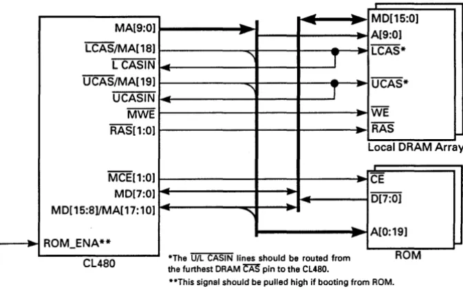
Figure 3-4 shows the signals that comprise the CL480's DRAM inter-face. The signal descriptions are presented following the figure. See Chapter 5 for more information about the DRAM memory architecture.
..
Figure 3-5
DRAM Interface
..
"" MD[15:0] MA[9:0] ""..
--
-A[9:0]
LCAS/MA[18]
--
---. LCAS*...
T
L CASIN--UCAS/MA[19] ...,
-
..
UCAS*T
-UCASIN
--MWE
..
-
WERAS[1:0] -'" RAS
"'"
Local DRAM Array
MCE[1:0]
-
CEMD[7:0]
-
D[7:0].. ~
MD[15:8]/MA[17:10]
"""
-""A[0:19] ROM_ENA**
CL480 the furthest DRAM * The U/L CASIN lines should be routed from CAS pin to the CL480.
--ROM
**This signal should be pulled high if a ROM is used.
DRAM Interface Signals
MA[9:0] - Memory Address Bus Outputs The CL480 multiplexes the row and column addresses on these signals to address up to one Mbyte of DRAM and uses address bits 9:0 for ROM addresses. See Chapter 5 for details of ad-dressing various DRAM components and DRAM array sizes.
MD[15:0] - Memory Data Bus Bidirectionals These signals comprise the memory data bus by which data is transferred between the CL480 and the local DRAMIROM ar-ray. AIl 16 bits are used in DRAM accesses, the direction of which is determined by the state of MWE.
For ROM accesses, MDATA[7:0] is the ROM data bus, and MDATA[15:8] becomes ROM address bits [17:10].
RAS[1 :0] - Row Address Strobe Outputs The CL480 asserts these signals to latch the row address into the DRAM array. RAS 1 (active low) latches the row address for bank 1, and RASO (low) latches the row address for bank O.
Video Interface
3.5
Video Interface
U<;AS-Upper Column Address Strobe
~ Lower Column Address Strobe
Output Output The CL480 asserts these signals to latch the column address into the DRAM array. UCAS (active low) latches the column address for the upper memory data byte, MD[15:8], and LCAS (active low) latches the address for the lower byte, MD[7:0]. UCAS is generated in response to the UDS input, and LCAS is generated in response to the LDS input.
Note: The LCAS and UCAS bits are also used as bits A[18] and A[19], respectively, in ROM accesses.
UCASIN -
Upper Data Latch EnableLcAsIN -
Lower Data Latch EnableInputs Inputs When the CL480 reads data from the local DRAM array, the data on MD[15:0] is latched into the CL480 on the rising edge of the two CAS IN signals. UCASIN latches data coming from the high data byte, MD[ 15: 8], and LCASIN latches data coming from the low data byte, MD[7:0]. Typically, these are connected to the UCAS and LCAS pins, respectively.
MWE - Write Enable Output
The CL480 asserts MWE (active low) during write operations (data transfer from CL480 to DRAM). The CL480 leaves MWE high during a read operation (DRAM to CL480).
MCE[1 :0] -Chip Enable Output
The CL480 asserts MCE (one for each ROM) during a read op-eration from ROM to the CL480.
ROM_ENA-Boot ROM Enable Input
Enables boot ROM. When this pin is high, the CL480 will ini-tialize itself with the data in ROM bank O.
The CL480's video interface outputs pixel data to the video display sub-system in ROB or YCbCr format. Figure 3-5 shows two possible con-figurations of the signals in the CL480's video interface: VSYNC/ HSYNC/VCK as outputs, and VSYNCIHSYNCNCK as inputs.
Note: depending on the video mode selected-RGB-24, YCb-Cr-16, and YCbCr-8-the pin count of the video interface varies, respectively, from 28, to 20, to 12 pins.
Operation of the video interface is discussed in Chapter 7.
VO /4/16/8
..
VCK ,
Video VSYNC
..
1
-
Unit HSYNC NTSC/PAL..
EncoderI
SignalI
VCK = 27 MHzGeneratorJ ,.
~
CL480
VO
Video Interface
I 24/16/8 ..
,
- NTSC/PAL Encoder [image:44.509.43.381.111.386.2]I
SignalI
GeneratorFigure 3-6
Video
---;::
Unit VSYNC
I
-.... HSYNC Video liming
...
+
VCK = 27 MHz GeneratorCL480
~
Video Interface Signals
VD[23:0] - Pixel Data Bus Outputs
The CL480 transmits pixel data to the video display subsystem using these signals. The definition of the signal lines differs for RGB and YCbCr formats as explained in Chapter 7.
HSYNC -
Horizontal Synchronization Bidirectional The CL480 begins outputting pixel data for a new horizontal line after the rising (inactive) edge ofHSYNC. HSYNC must be synchronous to VCK as shown in Chapter 7.VSYNC -
Vertical Synchronization Bidirectional The CL480 begins outputting the top border of a new field on the first HSYNC after the rising edge of VSYNC. VSYNC can be asynchronous with respect to VCK. See Chapter 7 for more information on the relationship of VSYNC to HSYNC.Audio Interfacte
3.6
Audio Interface
VOE - Video Output Enable Input
VOE must be asserted (active low) to enable the CL480 to drive the pixel bus, PD[23:0]. When VOE is deasserted, the CL480 puts the pixel bus in a high-impedance state (Note: This signal is active high in ESI).
VCK - Video Clock Bidirectional
VCK is derived from GCK and can be either an input or an out-put signal (which is independent of the direction ofVSYNC and HSYNC). VCK does not need to be synchronous with GCK.
The CL480's audio interface provides the reconstructed audio samples to the audio DACs. This bus complies with the usual three-wire (DA-BCK, DA-DATA, DA-LRCK) audio output. It also takes as input two external sources, DA-XCK and CDDA_EMP, and outputs DAC_EMP.
Figure 3-7
DA-DATA
-DA-LRCK
..
Audio DACs
DA-BCK
-DAC_EMP
- .
DA-XCK..
CDDA_EMPCL480
Audio Interface Signals
DA-DATA-Data Output
This signal outputs bit serial audio samples based on the DA-BCK clock.
DA-LRCK - Left-Right Clock Output
This signal identifies the channel for each audio sample.
DA-BCK - Bit Clock Output
DA-BCK is the audio bit clock. Divided by 8 from DA-XCK, it can be either 48 or 32 times the sampling clock.
DAC_EMP - Output Emphasis Flag Output In CD-DA pass-through mode, this signal is routed to the audio DACs.
DA-XCK - External Audio Frequency Clock Input Used to generate DA-BCK and DA-LRCK, DA-XCK can be ei-ther 384 or 256 times the sampling frequency.
CDDA_EMP - Input Emphasis Flag Input In CD-DA pass-through mode, this imput is directly routed to the DAC_EMP output pin.
Programmable I/Os
The CL480 provides programmable JlOs that may be used for control.
These IIOs become available by disabling the host interface
~:ogrammable
I/Os
(HOST_ENA=O) so that host interface pins may be used for controlfunctions as shown in the following tables.
Pin Name HSEL[O] HSEL[1 ]
Name/Function STOP/PLAY: 1 = Pause,
a
= PlaySCAN: 1 = Scan
vo
Note: In the table below, HD[O] and HD[I] perform the same functions normally set by SetMute().
HD[D] (MUTED)
a
1a
HD[1] (MUTE1) Attenuation on the PCM Samples
a
OdBo
-12 dB-00 (20 ms soft mute)
-12 dB
Programmable liDs
4
Host Interface
Functional
Description
The CL480's host interface, shown in Figure 4-1, is intended to provide a simple interface to an eight-bit microcontroller. The host interface provides three distinct functions:
o Coded data input (coded data may be sent through the host inter-face if the CD interinter-face is not used for this purpose)
o Local DRAMIROM access
o Internal register access
CL480
Host
CFlEVEL
Figure 4-1 CL480 Host Interface
4.1
Functional
Overview
Host Interface Registers
The host communication functions also include device initialization and microcode loading (if the ROM is not used). Host accesses to the CL480 can be asynchronous to GCK.
4.2
As shown in Figure 4-1, the host processor accesses CL480 resourcesHost Interface
by writing to address registers and reading or writing to data registers.Registers
A combination of five host interface registers are used:- - - 0 Three 8-bit address registers: A_MSB, A_MB, A_LSB
o Two 8-bit data registers: D_LSB and D_MSB
4.2.1 Host Interface Address Registers
The CL480's address registers allow the host to access the CL480's C-FIFO, local DRAM array or internal GBUS registers by setting A_MSB [7 :6], as shown in Table 4-1.
Table 4-1 Register Address Bits Used to Access DRAMJROM, C-FIFO, and GBUS
A_MSB[7:6] Data From/To
00 C-FIFO
01 DRAM/ROM (No autoincrementl
10 GBUS
11 DRAM/ROM (Autoincrementl
Thus the address register specifies which of four types of operations the CL480 can perform:
o Write to Code FIFO
o Read/write to GBUS (internal registers)
o Read/write to DRAM (external memory)
o Read/write to DRAM (external memory) with auto-increment ad-dressing
4.2.2 Host Interface Data Registers
The two host 8-bit data registers, D_LSB and D_MSB, are buffers be-tween the host bus and internal modules.
Transfers from the data registers to the destination specified by the ad-dress registers are triggered on the write operation to D _MSB and the read operation from D_MSB. Therefore, the write and read sequences are as follows:
o Write:
o Set address registers
o Write D_LSB register
o Write D_MSB register
DRead:
o Set address registers
DRead D _MSB register
DRead D_LSB register
Note: For back-to-back transactions to the C-FIFO, DRAM and internal registers, only the address bytes that differ from earlier transaction( s) need to be re-written a second time.
4.2.3 Accessing Host Interface Registers
The host accesses each of the five host interface registers by issuing a bus access with HSEL[2:0] set appropriately, as shown in Table 4-2.
Table 4-2 Summary of Host Interface Local Registers
HSEU2:0]' Register Name Contents
001 A_LSB Address, byte 0 (LSB)
010 A_MB Address, byte 1
011 A_MSB Address, byte 2(MSB)
100 D_LSB Data, byte 0 (LSB)
101 D_MSB Data, byte 1 (MSB)
1. Note: 000, 110 and 111 are illegal combinations which should not be used.
4.2.4 DRAMIROM Access
Bit 4 of A_LSB determines whether DRAM (set to 0) versus ROM (set to 1) is selected.
Host Interface Registers
Host Interface Registers
DRAM Access
When bit 6 of A_MSB is set to 1, the host sets A_MSB, A_MB, and A_LSB to form a 21-bit memory address as shown in Figure 4-2.
14
ROM Address ~r-
DRAM Address---J
DRAM171615 8 7 1 0
L...-_ _ _ _ _ _ _ _ • Auto-increment: 1
=
enabled, 0=
disabledFigure 4-2 DRAM/ROM Address Formed by Host Address Registers
This 21-bit memory address is a 16-bit word address, not a byte address. The address map is shown in Table 4-3.
Table 4-3 Memory Address Map
A_MSB[4] A_MSB[3] A_MSB[2] Memory Accessed
1 ROM Bank 1
1 0 ROM Bank 1
0 1 ROM Bank 0
0 0 ROM Bank 0
0 1 unused
0 0 unused
0 0 1 DRAM Bank 1
0 0 0 DRAM Bank 0
For DRAM accesses, bit 7 of Host address register A_MSB controls au-toincrementing. When autoincrementing is enabled (bit 7
=
1), each 16-bit data transfer between the host and the CL480 causes the DRAM ad-dress to be incremented to the next word.ROM Access
For access of ROM bank 0 versus 1, see Table 4-3. 4.2.5 Code FIFO Access
Host bus coded data may be sent to the CL480 in one of two basic modes:
o Serial mode (through the CD interface), as shown in Figure 4-3 and described further in Chapter 8.
o Parallel mode (through the host interface), as shown in Figure 4-4 and described in this section.
CL480
Figure 4-3 Sending Coded Data on CD Interface
CL480
Host Bus Host
Figure 4-4 Sending Coded Data on Host Interface
Host Interface Registers
Host Interface Registers
In code FIFO accesses through the Host interface, the Host specifies A_MSB[7:6]=00 as shown in Figure 4-6. Then the words written to D_MSB and D_LSB will transfer to the Code FIFO.
15 Coded Data FIFO 0
7 6 5
1
\
l
I
0
I
1 I 10101 X
D_MSB D_LSB
Figure 4-5 C-FIFO Register Address Formed by A_MSB
The CL480 can sustain a coded data input transfer rate of up to 2.5 Mbytes per second through the D _MSB and D _LSB registers. The C-FIFO holds 31 words, each of which is 16-bits wide.
4.2.6 Internal Register Access
If the Host specifies A_MSB [7 :6]= 1 0, then the access is an internal reg-ister access, as shown in Figure 4-6.
15 Selected Register
o
\
J
'---_---'I 1'---_---'
A_MSB D_MSB D_LSB
Figure 4-6 Internal Register Address Formed by A_MSB
Internal registers that are accessible by the host are listed in Table 4-3.
Host Interface Registers
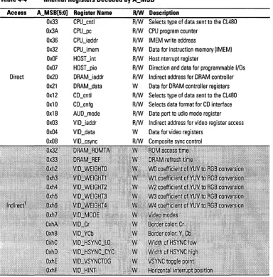
[image:54.505.44.428.120.510.2]Note: Registers are defaulted to the correct value through microcode initialization unless otherwise noted in the Con-figuration Area description given in Section 12.3.
Table 4-4 Internal Registers Decoded by A_MSB
Access A_MSB[5:0] Register Name R/W Description
Ox33 CPU_cntl Rm Selects type of data sent to the CL480
Ox3A CPU_pc Rm CPU program counter
Ox36 CPUjaddr Rm IMEM write address
Ox32 CPUjmem Rm Data for instruction memory (lMEM) OxOF HOSTjnt Rm Host nterrupt register
Ox07 HOST_pia Rm Direction and data for programmable liDs
Direct Ox20 DRAMjaddr Rm Indirect address for DRAM controller Ox21 DRAM_data W Data for DRAM controller registers Ox12 CD_cntl Rm Selects type of data sent to the CL480 Oxl0 CD_cnfg Rm Selects data format for CD interface OxlB AUD_mode Rm Data port to udio mode register Ox03 VIDjaddr Rm Indirect address for video register access Ox04 VID_data W Data for video registers
OxOB VID_csync Rm Composite sync control
1. Indirect register addresses are written to either DRAMjaddr or VlOjaddr.
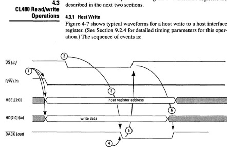
CL480 Read/write Operations
CL480 read and write operations using the host interface registers are
4.3
described in the next two sections.CL480 Read/write
os (in)
RtW(in)
HSEL[2:0]
HO[7:0] (in)
[image:55.507.27.469.75.366.2]OACK(ou~
Figure 4-7
Operations
4.3.1 HostWriteFigure 4-7 shows typical waveforms for a host write to a host interface register. (See Section 9.2.4 for detailed timing parameters for this oper-ation.) The sequence of events is:
Host Interface Local Register, Write Operation
1. The host drives RIW low to indicate a write operation. It also drives the host register address onto HSEL[2:0] and the write data onto HD[7:0].
2. When the HD[7:0], RIW and HSEL[2:0] lines have settled, the host processor asserts DS.
3. In response to the assertion of DS, the CL480 begins the write sequence and sometime later generates a DACK signal. 4. The CL480 latches the data when DACK goes low.
5. In response to the assertion of DACK, the host deasserts DS. 6. The CL480 responds by releasing DACK. This completes the
write cycle.
CL480 Read/write Operations
4.3.2 Host Read
Figure 4-7 shows typical waveforms for a host read from a host inter-face register. (See Section 4.4 for detailed timing parameters for this op-eration.) The sequence of events is:
CD
CD
os lin)
---~\~---~/~---RiW(in)
SEL[2:0]
HO[7:0] (in)
OACK(out)
Figure 4-8 Host Interface Local Register, Read Operation
1. The host drives RIW high to indicate a read operation and drives the host register address onto HSEL[2:0].
2. When the RIW and HSEL[2:0] lines have settled, the host pro-cessor asserts DS to indicate to the CL480 that a host bus read access is in progress.
3. In response to the assertion of DS, the CL480 holds DACK deasserted (high) until it can respond to the read request. Be-cause the CL480 is performing arbitration of its internal data buses during register access, DACK assertion is delayed at least one GCK cycle.
4. When the data is available, the CL480 asserts DACK and drives the data.
5. The host deasserts DS when the data has been read.
6. In response to the deassertion of DS, the CL480 releases DACK and D[7:0].
CL480 Read/write Operations
Chapter 5
DRAM/ROM
Interface
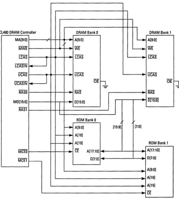
This chapter describes the local DRAMIROM Interface bus, shown in Figure 5-1, and how it is used. It details all of the signals necessary to connect the CL480 to a DRAM array and optional ROM.
The sections in this chapter are:
o 5.1, General Description
o 5.2, DRAM Memory Bus Interface
o 5.3, ROM Memory Bus Interface and Timing
o 5.4, DRAM Memory Bus Timing o 5.5, Memory Design Guidelines