DSD 890
User Guide
Copyright © 1983
All rights reserved. No part of this book may be reproduced in any form or by any means without prior written permission of Data Systems Design, Inc.
WARRANTY
Data Systems Design products are warranted against
defects in materials and workmanship. For DSD products sold in the U.S.A., this warranty applies for ninety (90) days from date of shipment.* DSD will, at its option, either repair or replace either equipment or components which prove to be defective during the warranty period. This warranty includes
labor, parts, and surface travel costs of system modules or components. Freight charges for other than surface travel or for complete systems returned for repair are not included in this warranty. Equipment returned to DSD for repair must be shipped freight prepaid and accompanied by a Material Return Authorization number issued by DSDCustomer Service. Repairs necessitated .by shipping damage, misuse of the equipment, or by hardware, software, or interfacing not provided by DSD are not covered by this warranty.
PREFACE
This guide provides user information for the Data Systems Design (DSD) 890, Winchester and Tape Storage System, and con-tains the following information:
• Chapter 1: Brief description and features
• Chapter 2: Specifications and operational requirements
• Chapter 3: Physical and functional descriptions
• Chapter 4: Unpacking instructions, controls and
indica-tors, installation instructions, and acceptance tests
• Chapter 5: Operating instructions
• Chapter 6: User maintenance
• Chapter 7: Field troubleshooting and service information
• Appendix A: GEMEXR Software User Guide
• Appendix B: DSDBR Software User Guide
• Appendix C: TSEXR Software User Guide
• Appendix D: RLEXR Software User Guide
• Appendix E: Bootstrap Program Listing
The material in this manual is subject to change without
notice. The manufacturer assumes no responsibility for any
errors, which may appear in this manual.
SAFETY
Operating and maintenance personnel must always observe sound safety practices. Do not replace components, or attempt
repairs to this equipment with the power turned on. Under cer-tain conditions, dangerous voltage potentials may exist when the power switch is in the off position, because of charges retained on capacitors. To avoid injury, always remove power before attempting repair procedures.
Data Systems Design, Inc. will accept no responsibility for injury or damage sustained as a result of operation or maintenance of this equipment with the covers removed and the power applied.
WARNING
This equipment generates, uses, and can radiate radio fre-quency energy and if not installed and used in accordance with
the instructions manual, may cause interference to radio com-munications. It has been tested and found to comply with the
limits for a Class A computing device pursuant to Subpart J of Part 15 of FCC Rules, which are designed to provide reasonable protection against such interference when operated in a com-mercial environment. Operation of this equipment in a
residen-tial area is likely to cause interference in which case the user at his own expense will be required to take whatever measures may be required to correct the interference.
CAUTION
Do not operate system until you have:
• Released the lock on the Winchester drive (spindle lock).
• Rotated the head lock actuator to RUN position.
Both locks are secured in a locked position before ship-ment from the factory. See Chapter 4 for detailed procedures covering installation and checkout of equipment.
IMPORTANT
Table of Contents 1. 1.1 1.2 1.3 2. 2.1 2.2 2.3 2.4 3. 3.1 3.2 3.3
4.
4.1 4.2 4.34.4
4.5 4.6INTRODUCTION
.
.
.
.
. . .
.
. .
. . .
.
.
.
.
. .
.
. . .
. .
.
.
. .
.
General InformationSystem Overview
. . . .
.
. .
. .
.
.
.
. . .
.
. .
. .
.
. . .
.
.
. . .
. . .
.
.
. . .
. . .
.
Fea tures •.•.•.••••••••••••••.•••••••••••.••••••••
SPECIFICATIONS
. . . .
.
. . .
. . . .
.
.
. . .
.
.
.
.
. . .
General Information ••••••••••••••••••••••••••••••System Modules ••••••••••••••••••••••••••••••••••• Recording Characteristics •••••••••••••••••••••••• Cable and Connector Requirements ••••••••••••••••• SYSTEM DESCRIPTION
. . .
. . .
. .
.
.
.
. . . .
.
. . .
.
.
.
. .
General Information ••••••••••••••••••••••••••••••Introduction . . . • . • . . .
Functional Description ••••••••••••••••••••••••••• 3.3.1 Disk Drive Emulation •••••••••••••••••••••• 3.3.2 Non-Interleaved Data Transfer ••••••••••••• 3.3.3 Error Detection and Correction •••••••••••• 3.3.4 Disk Flaw Management •••••••••••••••••••••• 3.3.5 Tape Drive Emulation •••••••••••••••••••••• 3.3.6 Tape Cartridge Storage Capacity ••••••••••• INSTALLATION
. .
.
. . . .
.
. .
.
. .
. .
.
. .
. .
. . .
.
.
.
.
. . .
.
General Information •••••••••••••••••••••••••••••• Unpacking and Inspection ••••••••••••••••••••••••• Controls and Indicators •••••••••••••••••••••••••• 4.3.1 Status Panel •••••••••••••••••••••••••••••• 4.3.2 Operator Panel •••••••••••••••••••••••••••• Power Requirements ••••••••••••••••••••••••••••••• Mechanical Preparations ••••••••••••••••••••••••••Installation . . . .
4.6.1 Cabinet Installation
.
. . .
. .
.
. .
. . .
.
. . .
. .
4.6.2 Cabling.
. .
.
. .
. . . .
.
.
. . .
. . .
. . .
.
.
4.6.3 Configuring Controller Board ••••••••••••••4.6.4
4.6.3.1 Bootstrapping Options •••••••••••• 4.6.3.2 Device Options ••••••••••••••••••• 4.6.3.3 Interrupt Priority Options ••••••• 4.6.3.4 DMA Request Monitor Option ••••••• 4.6.3.5 Error Correction Option •••••••••• Mounting Controller •••••••••••••••••••••••
5. 5.1 5.2 5.3 5.4 5.5 5.6 5.7 6. 6.1 6.2 6.3 6.4 7. 7.1 7.2 7.3 7.4 7.5 7.6 7.7 7.8 7.9
4.6.7 Installing Software Programs •••••••••••••• 4.6.7.1 Transfer Using Floppy •••••••••••• 4.6.7.2 Transfer Using RL02 •••••••••••••• 4.6.7.3 Transfer Using TSV05 ••••••••••••• OPERATING INSTRUCTIONS
. . .
. . .
.
.
.
. .
. . . .
.
.
. .
. . .
. .
General Information ••••••••••••••••••••••••••••••Introduction . . . • . . .
Applying Power ••••••••••••••••••••••••••••••••••• Loading the Cartridge •••••••••••••••••••••••••••• Unloading the Cartridge ••••••••••••••••••••••••••
Bootstrapping . . . • . . . • . . .
Backup and Restore Operations •••••••••••••••••••• 5.7.1 Creating Backups •••••••••••••••••••••••••• 5.7.2 Restoring Disk Data ••••••••••••••••••••••• USER MAINTENANCE
. .
.
.
. . .
. .
. . .
. .
.
.
.
.
. . .
.
.
. . .
General Information •••••••••••••••••••••••••••••• Proper ventilation ••••••••••••••••••••••••••••••• Cleaning the Cabinet ••••••••••••••••••••••••••••• Quick Troubleshooting Chart •••••••••••••••••••••• FIELD TROUBLESHOOTING AND REPAIRS. . .
. . . .
. .
.
.
.
. .
.
.
General Information •••••••••••••••••••••••••••••• Maintenance Philosophy ••••••••••••••••••••••••••• Preventive Maintenance ••••••••••••••••••••••••••• Winchester Disk Formatting ••••••••••••••••••••••• Bad-Track Map Updating ••••••••••••••••••••••••••• Diagnostic Tools ••••••••••••••••••••••••••••••••• 7.6.1 Power-On Confidence Tests •••••••••••••••••7.6.2
7.6.1.1 Winchester POCs •••••••••••••••••• 7.6.1.2 Tape Drive POCs ••••••••••••••• 7.6.1.3 POCs Results
. . .
.
. .
.
. .
.
.
.
. . .
HyperDiagnostics •••••••••••••••••••••••••• 7.6.2.1 Controls and Indicators •••••••••• 7.6.2.2 Description •••••••••••••••••••••• 7.6.2.3 Operation ••••••••••••••••••••••••Troubleshooting •••.••••••••••••••••••••••••••••
Replacement Procedures •••••••••••••••••••••••••••
7.8.1 Preparation . . . • • . . . • . . .
7.8.2 Replacing Modules ••••••••••••••••••••••••• Maintenance Assistance ••••••••••••••••••••••••••• APPENDIX A: GEMEXR UTILITY PROGRAM •••••••••••••••••••••
List of Figures
Figure 2-1. Syste~ Modules ••••••••••••••••••••••••••••
Figure 3-1. DSD 8240 Controller Board ••••••••••••••••• Figure 3-2. Controller Architecture ••••••••••••••••••• Figure 3-3. DSD Winchester/RL02 Emulation ••••••••••••• Figure 3-4. Two-Port RAM Buffer Data Transfer ••••••••• Figure 4-1. Status Panel •••••••••••••••••••••••••••••• Figure 4-2. Operator Panel •••••••••••••••••••••••••••• Figure 4-3. Winchester Spindle and Head Lock •••••••••• Figure 4-4. Front Bezel Removal ••••••••••••••••••••••• Figure 4-5. Cabinet and Board Cabling ••••••••••••••••• Figure 4-6. DSD 8240 Jumpers •••••••••••••••••••••••••• Figure 4-7. Bootstrapping Options ••••••••••••••••••••• Figure 4-8. Device Options •••••••••••••••••••••••••••• Figure 4-9. Interrupt priority Options •••••••••••••••• Figure 4-10. DMA Request Monitor Option ••••••••••••••• Figure 4-11. Error Correction Option •••••••••••••••••• Figure 4-12. Common LSI-11 Backplanes ••••••••••••••••• Figure 4-13. Transferring Software Using Floppy ••••••• Figure 4-14. Transferring Software Using RL02 ••••••••• Figure 4-15. Transferring Software Using TSV05/TSll ••• Figure 5-1. Magnetic Tape Cartridge ••••••••••••••••••• Figure 5-2. Inserting the Cartridge ••••••••••••••••••• Figure 6-1. Fuse Location ••••••••••••••••••••••••••••• Figure 7-1. Tape Drive Cleaning ••••••••••••••••••••••• Figure 7-2. HyperDiagnostics Controls and Indicators •• Figure 7-3. HyperDiagnostics Procedure •••••••••••••••• Figure 7-4. Main Troubleshooting Path ••••••••••••••••• Figure 7-5. POC Failure ••••••••••••••••••••••••••••••• Figure 7-6. Bootstrapping Failure ••••••••••••••••••••• Figure 7-7. Power Distribution Diagram •••••••••••••••• Figure 7-8. Cabinet Exploded View •••••••••••••••••••••
List of Tables
Table 2-1. System Modules ••••••••••••••••••••••••••••• Table 2-2. System Specifications •••••••••••••••••••••• Table 2-3. Cabinet Specifications ••••••••••••••••••••• Table 2-4. Interface Specifications ••••••••••••••••••• Table 3-1. Block Size vs Tape Storage Capacity •••••••• Table 4-1. Status Panel--Indicators ••••••••••••••••••• Table 4-2. Operator Panel--Controls and Indicators •••• Table 4-3. DSD 8240 Jumpers ••••••••••••••••••••••••••• Table 5-1. Bootstrap Device Selection ••••••••••••••••• Table 6-1. Quick Troubleshooting Chart •••••••••••••••• Table 7-1. HyperDiagnostics Tests ••••••••••••••••••••• Table 7-2. HyperDiagnostics Error Codes ••••••••••••••• Table 7-3. Software Diagnostic Procedures ••••••••••••• Table 7-4. POC Error Codes •••••••••••••••••••••••••••• Table 7-5. Bootstrap Error Codes •••••••••••••••••••••• Table 7-6. Error Code Summary •••••••••••••••••••••••••
DATA SYSTEMS DESIGN
--
--~
I~---~DSD 89@ Winchester and Tape Storage System
1 INTRODUCTION
1.1. General Information
This chapter briefly describes the DSD 890 Winchester and Tape Storage System and outlines its features. Refer to Chapter 3 for a more comprehensive description.
1.2. System Overview
The DSD 890 is a mass storage system consisting of a main cabinet and an intelligent bus interface board. The system is fully compatible with DEC computers using LSI-ll bus confi-gurations and provides, in a rack-mount package, many value-added features not found in comparable DEC equipment. For example, the cabinet contains:
• An eight-inch Winchester (sealed bubble) disk drive. This
drive replaces three DEC RL02 cartridge disk volumes, storing up to 31.2 Mbytes of formatted data.
• A start/stop Tape drive that uses 1/4-inch tape
car-tridges. This drive stores up to 16.25 Mbytes of format-ted data on each cartridge and emulates DEC TSll/TSV05-class subsystems. The DSD Tape drive can be used to
obtain backup copies of Winchester disk data, restore the data, or load diagnostic programs distributed by DSD.
In addition, the cabinet contains its own power supply, a built-in bootstrapping program, and cooling fan. Switches and LEOs are conveniently located on the front panel to permit:
• individual write-protection of each of the three
Winches-ter volumes.
• control over Tape cartridge load/unload operations.
• rapid access to comprehensive HyperDiagnostics - a DSD
The cabinet is interfaced with DEC LSI-II computers via the DSD 8240 Controller board. This quad-wide board is
hardware compatible with all DEC LSI-II bus (Q-Bus) back-planes. The board is, both, a bus interface for the storage cabinet and an intelligent controller that emulates DEC RL02, and TSll/TSV05 auxiliary storage subsystems, allowing the user to fully utilize operating systems and application software distributed by DEC.
This board contains a high-speed direct memory access (DMA) microcontroller and three gate arrays that provide non-interleaved disk operations, transparent error correction, and optimum system throughput.
1.3. Features
The following list compiles features of the DSD 890 System: Winchester Drive
• Emulates three DEC RL02 disk pack subsystems.
• Provides three 10.4-Mbyte storage volumes.
• Contains built-in bootstrapping PROM.
• Supports 22-bit addressing modes.
• Provides HyperDiagnostics via Operator panel.
Tape Drive
• Emulates one DEC TS-ll/TSV05 (1/2-inch) tape subsystem.
• Provides up to 16.25 Mbytes of back-up storage on each
cartridge.
• Supports 22-bit addressing modes.
• Provides HyperDiagnostics via Operator panel.
Controller Interface Board
• Fully emulates DEC peripheral controllers.
• Provides software compatibility with DEC LSI-ll (Q-Bus)
computers.
• Provides compatibility with RT, RSX, TSX, TSX+, RSTS, and
UNIX operating systems.
• Uses one of two user-selectable methods for transferring
disk sector data: Two-way interleaving method afford flexibility, while non-interleaving method results in increased data throughput rate
• Supports simultaneous disk and tape operations with
max-imum throughput and minmax-imum degradation of either opera-tion.
• Corrects Winchester drive error bursts up to 11 bits long
using error correction coding (ECC) techniques.
• Detects Tape drive random errors using a 16-bit cyclic
redundancy coding (CRC) technique.
• Supports DSD diagnostic software for testing storage
dev-ices and media.
• Supports DSD software utilities for managing Winchester
media, for making backup copies of Winchester volumes on cartridge, and for restoring cartridge data to Winchester volumes.
• Uses state-of-the-art semiconductor technology on single
quad-wide controller board.
• Provides increased reliability and serviceability, at
reduced cost.
• Complies with LSI-ll bus bandwidth requirements.
• Provides automatic error retry for Winchester disk data.
• Provides access, via computer console, to DEC on-line
debugging techniques (ODT).
2 SPECIFICATIONS
2.1. General Information
This chapter outlines specifications and operational require-ments for the DSD 890 Winchester and Tape Storage System. Specifications include storage capacities, recording charac-teristics, and data transfer rates. Also provided is a listing of major components and the system physical dimensions.
Requirements include interface cabling, connectors, and power requirements. Environmental limitations are also stated.
2.2. System Modules
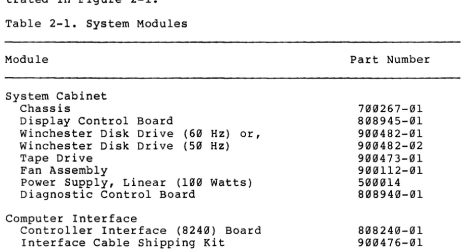
The DSD 890 System modules are listed in Table 2-1 and illus-trated in Figure 2-1.
Table 2-1. System Modules
Module
System Cabinet Chassis
Display Control Winchester Disk Winchester Disk Tape Drive
Fan Assembly
Board Drive Drive
(60 Hz) (50 Hz)
or,
Power Supply, Linear (100 Diagnostic Control Board
Watts)
Computer Interface
Controller Interface (8240) Board Interface Cable Shipping Kit
Part Number
700267-01 808945-01 900482-01 900482-02 900473-01 900112-01 500014 808940-01
[image:15.617.88.543.403.651.2]POWER SUPPLY
1/4" CARTRIDGE TAPE
STATUS DISPLAY CONTROL PANEL
[image:16.612.49.552.189.506.2]2 1 System Modules
Figure - .
COOLING FAN 31.2 Mbyte WINCHESTER DISK
DRIVE
SD 8240 QUAD·WIDE CgNTROLLER 1 INTERFACE
2 • 3 • Recording Characteristics
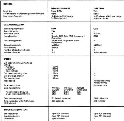
The Winchester drive records data using the modified frequency modulation (MFM) technique. The magnetic tape cartridge drive uses the group code recording (GCR) technique. Product specif-ications are listed in Tables 2-2 through 2-4.
Table 2-2. System Specifications
GENERAL
WINCHESTER DRIVE TAPE DRIVE
Emulates Three RL02s T5-11
Modifications to Operating System Software None None
Formatted Capacity 10.4 Mbyles/RL02 image 16.25 Mbyles (450 ft. cartridge. 31.2 Mbyles total 16 Kbyle blocks)
DATA ORGANIZATION
Recording technique MFM GCR
Bytes'disk sector 256
-Bytes,tape bloc\<
-
512-16KError detection Header CRC Data ECC. Transparent CRC Correction
Flaw management Spare track assignment is user -transparent
Recording density 6600 bpi 6400 bpi
Track density 345tpi
-Number of read/write heads 8 1
Number of tracks 512 4 (Serpentine)
SPEEDS
Disk seek lime (including head setting)
65 ms
Average
-Maximum 100 ms
-Track-to-track 15 ms
-Disk head switching time 20 ms
-Disk average latency 10 ms
-Disk start-up time 30 sec.
-Tape speed 30 ips (read/write)
70 ips (rewind)
Tape rewind time 3 minutes max.
Data transfer time WITHIN A WITHIN A ACROSS SECTOR CYLINDER ENTIRE DISK Non-interleaved Kbyte/s 542.5 396.8 352.7 2-way interleaved Kbytels 542.5 198.4 186.7
Data transfer length 5.1 Kwords maximum 256 to 8 Kwords Time to read or write RL02 Image 25.5 seconds 8.95 minutes (10.4 Mbytes)
ERROR RATES (W/O ECC)
Soft read errors 1 per 10'· bits read 1 per 10'· bits read Hard read errors 1 per 10" bits read 1 per 10" bits read
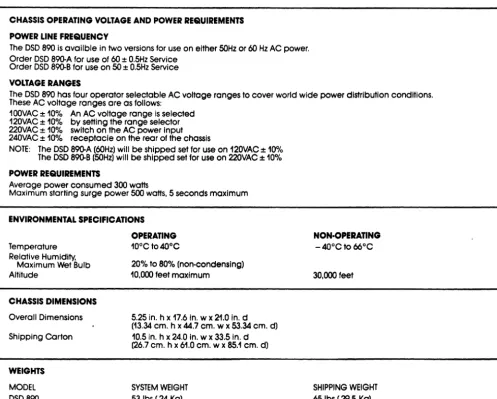
[image:17.618.63.568.206.696.2]-Table 2-3. Cabinet Specifications
CHASSIS OPERATING VOLTAGE AND POWER REQUIREMENTS
POWER LINE FREQUENCY
The DSD 890 is availble in two versions for use on either 50Hz or 60 Hz AC power. Order DSD 890-A for use of 60 ± 0.5Hz Service
Order DSD 890-B for use on 50 ± 0.5Hz Service
VOLTAGE RANGES
The DSD 890 has four operator selectable AC voltage ranges to cover world wide power distribution conditions. These AC voltage ranges are as follows:
100VAC ± 10% An AC voltage range is selected 120VAC ± 10% by setting the range selector 220VAC ± 10% switch on the AC power input 240VAC ± 10% receptacle on the rear of the chassis
NOTE: The DSD 890-A (60Hz) will be shipped set for use on 120VAC ± 10% The DSD 890-B (50Hz) will be shipped set for use on 220VAC ± 10%
POWER REQUIREMENTS
Average power consumed 300 watts
Maximum starting surge power 500 watts, 5 seconds maximum
ENVIRONMENTAL SPECIFICATIONS
OPERATING
Temperature Relative Humidify.
Maximum Wet Bulb Altitude CHASSIS DIMENSIONS Overall Dimensions Shipping Corton WEIGHTS MODEL DSD890
10°C to 40°C
20% to 80% (non-condensing) 10,000 feet maximum
5.25 in. h x 17.6 in. w x 21.0 in. d (13.34 cm. h x 44.7 cm. w x 53.34 cm. d) 10.5 in. h x 24.0 in. w x 33.5 in. d (26.7 cm. h x 61.0 cm. w x 85.1 cm. d)
SYSTEM WEIGHT 53 Ibs ( 24 Kg)
Table 2-4. Interface Specifications
LSI-11 INTERFACE
WINCHESTER DRIVE
Backplane Requirement One quad-wide Q-Bus slot Device Address
in any Q.Bus backplane
Standard 1m4400
Alternate 1m4420
Interrupt Address
Standard 160
Alternate 150
Bootstrap Address
Standard 1m3000
Alternate 1m1000
NON'()PERATING
- 40°C to 66°C 30,000 feet
SHIPPING WEIGHT 65 Ibs ( 29.5 Kg)
TAPE DRIVE
1m2520 1m2530
[image:18.623.49.547.100.499.2]2.4. Cable and Connector Requirements
The DSD 890 System is furnished with all internal cables installed and configured for proper operation. The DSD 8240 controller interface board is installed at the backplane of the host computer and connected to the system cabinet by three cable assemblies:
(a) A 50-pin Winchester control cable
(b) A 20-pin Winchester data cable
(c) . A 40-pin Tape cable
3 SYSTEM DESCRIPTION
3.1. General Information
This chapter describes the DSD 890 System. Emphasis is given to the DSD 8240 board, which provides computer interfacing and control of all data storage and retrieval operations.
3.2. Introduction
The DSD 890 is a mass storage system that consists of a Win-chester drive, a Tape drive, and a DSD 8240 Controller board.
Designed to support the DEC LSI-ll computer product line, the DSD 890 System emulates interface software of DEC RL02 and TSll/TSV05 subsystems.
The LSI-ll (Q-Bus) bus uses 44 lines. These lines are used by the central processing unit (CPU), main memory, and input/output (I/O) devices to communicate with each other.
Most lines are bidirectional and use terminations for maintaining a high (negated) transistor-transistor-logic (TTL)
level. Devices are connected to these lines via high impedance bus receivers and open collector drivers. A device can assert a line when its driver places a low TTL logic level on the line.
All devices on the bus communicate with each other in an asynchronous mode. For bus transactions between devices to occur, one device must become master and the other become slave. Some devices, such as main memory are always slave.
A device, such as disk or tape, can become master by asserting a DMA-request signal to request the data section of the bus. The CPU is responsible for arbitrating simultaneous requests and granting the bus to the device with highest priority.
This method is most useful when using mass storage dev-ices that move large blocks of data to and from main memory. DMA causes the least intervention from the CPU and it is con-sequently the most efficient data transfer method.
During DMA, the storage device needs to know the starting address in memory, the starting address in the storage device, the length of the transfer, and the type of operation. DMA starts after the CPU grants bus mastership to the highest priority DMA device requesting the bus.
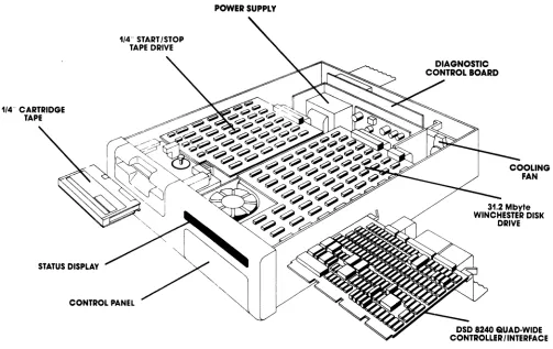
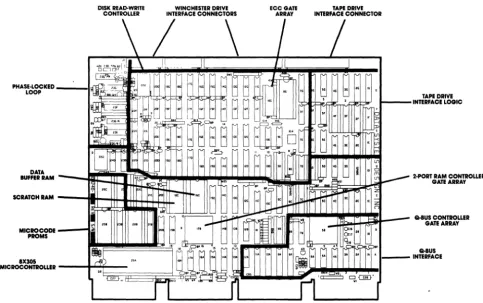
The DSD 890 contains an intelligent interface controller that uses a microcontroller and three semi-custom designed gate array integrated circuits (IC) for emulating DEC software while providing full compatibility (see Figure 3-1).
The microcontroller, a Signetics 8X305, is a high-speed processing device, which performs and controls all the intel-ligent functions of the storage system.
The microcontroller receives commands from the LSI-ll computer intended for the specific peripheral devices. These commands are coded into a form compatible with the DSD storage devices and transmitted to them.
Similarly, the microcontroller receives data from the storage devices and codes the data into a format compatible with the LSI-ll operating software.
Gate arrays are large scale integrated (LSI) circuits fabricated by a process, which provides designers with cir-cuits semi-customized to their application. Using gate arrays results in a more efficient and cost-effective product.
The DSD 890 uses three gate array devices to provide several product enhancements. Use of these devices allow the following value-added features:
• Non-Interleaved Disk Operation: Increased data transfer
rate, across the entire disk, to 352.7 Kbytes per second
- about 12 percent faster than a single RL02 subsystem.
• Transparent Error Correction: Detection of error bursts
22 bits long and correction of 11 bits. These functions are performed transparently.
• Optimum System Throughput: DMA is used to obtain greatest
DISK READ-WRm
CONTROUER INTERFACE CONNECTORS WINCHESTER DRIVE ECCGATE ARRAY
\/
\
I
Figure 3-1. DSD 8240 Controller Board
TAPE DRIVE INTERFACE CONNECTOR
/
TP 316/83
_ Q.8US CONTROUER
[image:23.620.57.540.164.467.2]The Winchester is a Quantum Q2040 eight-inch Winchester disk drive. The Tape is a Kennedy 6455 1/4-inch start/stop cartridge tape drive.
The Winchester drive stores a maximum of 31.2 Mbytes of formatted data. The data transfer rate within a sector, within a cylinder, or across the entire disk varies with the method used for transferring data (i.e., non-interleaving or two-way interleaving). Refer to Chapter 2, Specifications for more details.
The Tape has four tracks arranged in a serpentine confi-guration. Data is recorded serially, and reading/writing takes place in both directions with an automatic head switch at the end of the tape. The data transfer rate is 24 Kbytes per
second.
Because of recording overhead, the Tape storage capacity is directly related to the block size used in the recording
format. The storage capacity ranges from 3.56 Mbytes to 16.25
Mbytes.
3.3. Functional Description
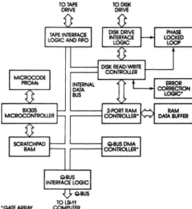
The DSD 8240 Controller consists of a 8X305 microcontroller connected to a high-speed internal data bus, three gate
arrays, a disk read/write controller chip, and tape interface logic with first-in-first-out (FIFO) buffers. (See Figure 3-2.)
The 8X305 is a bipolar microcontroller with a cycle time of 200 ns. The 8X305 serves as internal bus master and con-trols all on-board intelligent functions; for example:
• Monitors and controls Winchester drive, tape drive, and
interfacing operations.
• Performs the storage device emulation function.
• Provides read, write, and data transfer functions.
8X3Q5 MICROCONTROLLER
TO TAPE DRIVE
INTERNAL DATA BUS
TOOISK DRIVE
PHASE LOCKED
LOOP
ERROR '---~ CORRECTION
LOGlCo
RAM
DATA BUFFER
Q.BUSDMA r---fCONTROLLERo
o GATE ARRAY
TO LSI-11 COMPUTER
Figure 3-20 Controller Architecture
[image:25.617.162.443.152.457.2]The disk read/write controller, tape interface logic, two-port RAM controller, and Q-Bus DMA controller act as internal bus slaves. Disk data is synchronized by a phase-locked loop, under control of the read/write controller.
During device operation, the 8X305 produces a status for each device and stores it in RAM. As disk and tape operations proceed, the 8X305 updates and stores various bits of
informa-tion.
Any read of the I/O registers by the computer software interrupts the 8X305 and causes it to place, within ten
microseconds, the selected register data on the Bus. This high speed is required to avoid an abort of the operation by the LSI-II watchdog timer.
The use of intelligence in the DSD 8240 Controller allows a single quad-wide board to emulate two different storage dev-ices, and to provide additional features such as
non-interleaved data transfer, transparent error detection and correction, disk flaw management, and on-board diagnostics.
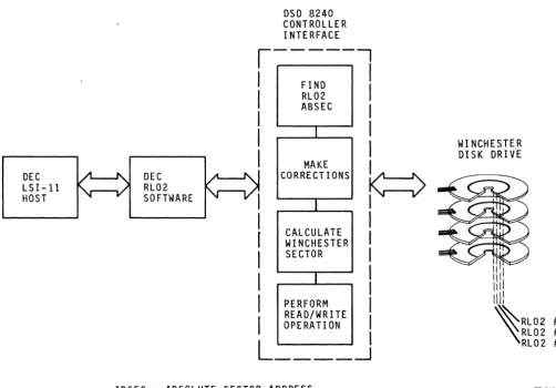
3.3.1. Disk Drive Emulation
The DSD Controller emulates three l0.4-Mbyte RL02 drives using an eight-inch Winchester drive.
The RL02 disk drive has two read/write heads, one on each side of a single disk-platter. Each side of the platter has 512 concentric tracks. Each track contains forty 256-byte sec-tors.
The DSD Winchester drive has eight read/write heads, one on each side of four platters. Each side of a platter has 512 tracks. Each track contains thirty-one 256-byte sectors.
Because of the physical differences between the two drives, the Controller needs to convert track, head, and
sec-tor addresses of the RL02 drives to a form compatible with the Winchester drive.
To emulate the drives, the Controller maps the RL02s vertically as three concentric, three-dimensional cylinders, instead of assigning each Winchester platter a different RL02.
DEC LSI-ll HOST
DEC RL02 SOFTWARE
DSD 8240 CONTROLLER INTERFACE
,---,
I
I
I
I
I
I
FIND RL02 ABSEC
I
I
I
I
I
MAKE CORRECTIONS
I
CALCULATE WINCHESTER SECTOR
I
PERFORM
b
I
I
I
I
I
I
I
I
I
I
READ/WRITE OPERATION
L ____
---1
ABSEC
=
ABSOLUTE SECTOR ADDRESSFigure 3-3. DSD Winchester/RL92 Emulation
WI NCHESTER DISK DRIVE
[image:27.620.56.559.186.536.2]The following paragraphs describe the conversion process
used by the Controller:
(1)
The absolute sector number (ABSEC) is determined. RL02
disk addresses are re-defined to consist of a cylinder
number (CY), a head number (HD), and a sector number
(SEC). Head numbers range from 0 to 1; sector numbers
from 0 to 39. The firmware in the microcontroller uses
the following formula:
•
ABSEC
=
SEC
+
(40 x HD)
+
(80 x CY)
(2)
Corrections are made. An offset is added to identify the
RL02 being accessed and a correction for flaws is made
based on a flaw translation table stored on track 0 of
the Winchester drive.
(3)
The sector number is calculated. The result obtained
above is divided by a constant (248), yielding the
Win-chester drive cylinder number and a remainder. This
remainder is divided by another constant (31), yielding
the Winchester drive head number and a another remainder.
This second remainder is the Winchester sector number.
This number is added to another constant, which
identi-fies the RL02 volume being addressed.
(4)
A read or write operation is done. Using the information
obtained in the last step, the firmware commands the
Win-chester drive to position its head over the proper track
and read or write.
Using a similar process, responses from the Winchester
are converted into the format expected by the LSI-ll operating
system. Data is transferred between drive and main memory by
DMA.
3.3.2.
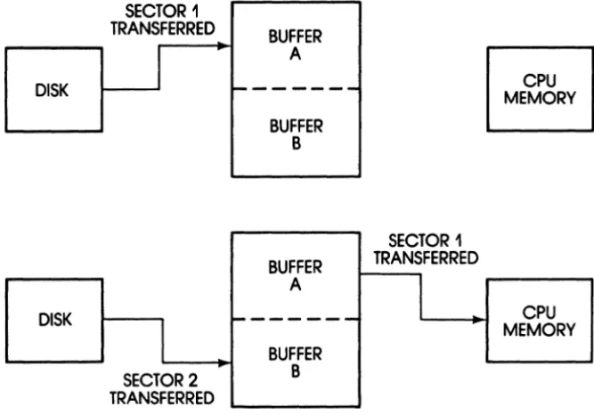
Non-Interleaved Data Transfer
The Controller is capable of transferring Winchester disk data
at an optimum rate by using non-interleaved data transfer
techniques; that is, reading or writing a full track of data
during one disk revolution.
SECTOR 1
TRANSFERRED BUFFER
I
ADISK
r---BUFFER B
SECTOR 1 BUFFER TRANSFERRED
A
I
DISK
---I
BUFFER SECTOR 2 B TRANSFERREDFigure 3-4. Two-Port RAM Buffer Data Transfer
CPU MEMORY
CPU MEMORY
[image:29.618.139.473.285.518.2]The control logic for the two-port RAM resides in a semi-custom gate array, which uses 1700 gates to do the equivalent function of 30 TTL devices.
The two-port buffer configuration allows Winchester sec-tor data to be read into one port, while data from the previ-ous sector is transferred to main memory. Figure 3-4 shows the details of the data transfer operation as-follows:
(1) When buffer A is filled with data from the first Win~hes
ter sector, the two-port RAM controller switches to
buffer B and begins to fill it with data from the second Winchester sector.
(2) As buffer B is being filled, the contents of buffer A are transferred to main memory.
(3) When buffer B is filled, the cycle is repeated and data moves continuously, at high speed, between disk drive and main memory.
If the CPU data bus is being used by other high data rate DMA devices, the high data rate transfer obtained by
non-interleaved operations may not be desirable. In such cases, the disk can be formatted for interleaved operations and the Controller set to slow down memory accesses for preventing I/O bus overloads.
3.3.3. Error Detection and Correction
A major DSD 8240 Controller feature is detecting and
correct-ing disk errors transparently; that is, in ~way not perceived
by the operating system.
The Controller contains a proprietary, complementary-MOS (CMOS) gate array that uses 540 silicon gates to provide error detection and correction.
The Controller implements these functions as follows:
(1) The 256-byte data record in a winchester sector is
con-verted to a binary polynomial of degree equal to the bits in the record.
(2) This polynomial is divided by a second constant
(3) The ECC is concatenated (appended) to the disk sector data each time a Winchester sector is written. When a sector is read, data and ECC are shifted through the chip. If no error is present, the remainder in the chip is equal to zero.
(4) If an error is present, the residual remaining in the
chip generates an error indication. This indication is used by the 8X305 microcontroller to generate an error pattern and to identify the location of the bit or bits in error.
(5) Once the error location is identified, the 8X305
micro-. controller attempts to reread the data record several times before applying error correction.
(6) If the error pattern persists, the 8X305 microcontroller
corrects the data in its data buffer before loading it into the host CPU memory, thus providing transparent error detection and correction of error burst up to 11 bits long.
3.3.4. Disk Flaw Management
Winchester disk drives contain permanent hard errors known as flaws. A list of these flaws is provided by the manufacturer with each drive. This list is used by DSD to produce a "bad-track map" table. Several copies of this table are then recorded in track 0 of the disk drive.
When power is applied, the DSD 8240 Controller reads the Winchester drive bad-track map table and stores it in scratch pad RAM.
After converting an RL02 disk address to a Winchester disk address, the 8X305 microcontroller accesses the bad-track map table from memory and compares its entries to the desired Winchester disk address. The microcontroller then makes the necessary corrections to ensure that complete tracks are flagged as defective and are not used.
3.3.5. Tape Drive Emulation
The DSD 8240 Controller emulates a DEC TS-ll or TSV05 magnetic tape system using a start/stop Tape drive.
The TS-ll/TSV05 tape drives use standard 1/2-inch, nine-track magnetic tape. The drives read and write at 25 inches per second, with a data transfer rate of 40 Kbytes per second.
The DSD Tape drive uses a smaller 1/4-inch, start/stop magnetic tape cartridge. Data is recorded serially at a
transfer rate of 24 Kbytes per second.
The 8X305 microcontroller receives LSI-II commands
intended for the DEC drive. These commands are converted into a form compatible with the Tape drive and are transmitted to it. Similarly, the 8X305 converts Tape drive data into the format expected by the computer.
3.3.6. Tape Cartridge storage Capacity
The DSD 890 Tape drive records data at 6.4 Kbits per inch (800 bytes per inch), using four serial tracks arranged in a ser-pentine configuration to avoid rewinding at the end of each track. The length of the tape in the cartridge is 450 feet
(5400 inches).
The unformatted capacity of a tape cartridge is computed by using the following formula:
• Storage Capacity
=
Bytes/inch x Tracks x Length; in ourcase this is: 800 x 4 x 5400
=
17.28 MbytesIn the Tape drive, data is recorded in blocks with an inter-block gap (IBG) of 1.2 inches. The data format on the tape for a single data block consists of the IBG, an 80-bit preamble, a 5-bit sync mark, the data pattern, a 5-bit end mark, a 16-bit CRC, and an 80-bit post-amble.
The formatted data (except data pattern) and the IBG are considered recording overhead. In our case, 186 bits (0.029) plus 1.2 inches of IBG for a total of 1.229 inches of over-head.
Table 3-1. Block Size vs Tape Storage Capacity BLOCK SIZE (Bytes)
256 512
1K 2K
4K 8K
16K
STORAGE CAPACITY (Mbytes)
[ A ]
3.56
5.91
8.80 11. 65
4 INSTALLATION
4.1. General Information
This chapter provides instructions for installing your 899 System, including acceptance test procedures.
The DSD 890 System is fully tested before shipping. Unless there is physical damage from shipment, it can be installed and made operational in a short period of time without any special procedures other than those recommended here.
4.2. Unpacking and Inspection
When your DSD 899 System arrives, inspect the shipping con-tainer immediately for evidence of mishandling during transit. If the container is damaged, request the presence of the
carrier's agent before opening it.
Compare the packing list attached to the shipping con-tainer against your purchase order to verify the shipment is correct.
Ensure that all items are unpacked and none accidentally discarded with the packing material. Note that the DSD 8249 Controller board is packaged in the shipping container
separately.
Carefully unpack the shipping container and inspect each item for external damage such as broken controls and connec-tors, dented corners, bent panels, scratches, or loose com-ponents.
If damage is evident, notify DSD Customer Service Depart-ment immediately.
4.3. Controls and Indicators
The controls and indicators are located on the front bezel of the system cabinet and consist of a Status display panel and an Operator panel.
The only control not accessible from the front bezel is the POWER ON/OFF switch, which is a rocker arm switch located at the rear of the cabinet.
4.3.1. Status Panel
The Status panel is located on the upper right side of the front bezel and becomes visible when the system cabinet is powered-up.
The Status panel shows the status of the Winchester and the Tape drives. It also provides system power on/off and fault indications.
The Status panel indicators are shown in Figure 4-1 and their functions described in Table 4-1.
Table 4-1. Status Panel - Indicators
Indicator Function
POWER
•
Lights to show cabinet is powered-upWIN
•
Lights to show Winchester drive is active ACTIVEWIN WP
•
Lights when any WIN VOLUME WRITE PROTECT switch is ONFAULT
•
Lights to show system fault (see Chapter 7 for details)TAPE
•
Lights to show Tape drive is active ACTIVEUNLOAD TAPE
ACTIVE FAULT WINWP
Figure 4-1. Status Panel
WIN
ACTIVE POWER
TP 326/83
4.3.2. Operator Panel
The Operator panel is located on the front bezel lower right side behind a hinged door. This door is opened by applying fingertip pressure near the bottom.
The Operator panel allows the operator to control Win-chester write-protect functions, tape load/unload operations, and to start HyperDiagnostics (see Caution below). It also provides diagnostic error code information.
The Operator panel controls and indicators are shown in Figure 4-2 and their functions described in Table 4-2.
Table 4-2. Operator Panel - Controls and Indicators
Control/Indicator
WIN VOLUME WRITE PROTECT (0 - 2) Switches
TAPE LOAD/UNLOAD Switch
TEST Pushbutton (momentary-action)
STATUS Indicator
Function
• Each, when set (ON), write-protects
corresponding drive volume and lights WIN WP indicator. (See Chapter 7 for other functions.)
• Setting to LOAD moves cartridge
to load point.
• Setting to UNLOAD moves cartridge to
unload point, lights UNLOAD indicator, and allows safe cartridge removal.
• Used for starting HyperDiagnostics.
(See Caution below.)
• Displays zero when system is off-line.
• Blanks when system is on-line.
(For other functions, see Chapter 7)
CAUTION: Some HyperDiagnostics (tests) will destroy
HYPERDIAGNOSTICS'·
I
D
0STATUS TEST
[
8
LOAD
1
ON
8
08
18
2UNLOAD OFF
TAPE WIN VOLUME WRITE PROTECT
TP 327/83
4.4. Power Requirements
The DSD 890 System is available in configurations for nominal line voltages of 120 or 240 Vac. The line frequency must be within 0.5 Hz of the required frequency (50 Hz or 60 Hz).
The system voltage and frequency configurations can be field-modified; however, the process requires that mechanical, as well as electrical, adjustments be made.
Should you need to modify the system, contact DSD Custo-mer Service for assistance.
4.5. Mechanical Preparations
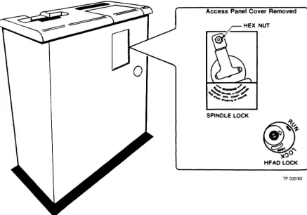
The system Winchester drive is shipped with locked spindle and head mechanisms. These mechanisms must be unlocked before
installation to avoid damage to the drive motor. Refer to
Figure 4-3 and follow these instructions:
(1) Remove spindle-lock access panel in bottom cover.
(2) Loosen 11/32" hex nut on spindle-lock.
(3) Rotate locking clip away from pulley.
(4) Tighten 11/32" hex nut.
(5) Replace spindle-lock access panel.
(6) Unlock head lock by rotating actuator lock
counterclock-wise to RUN (about I/2-turn). DO NOT FORCE. The Winches-ter drive is ready for operation. (See Caution below.)
CAUTION: Never ship the system cabinet or the Winchester
drive assembly with the spindle and head mechanisms unlocked.
SPINDLE LOCK
Figure 4-3. Winchester Spindle and Head Lock
Removed
~
ef;J ..,.
"
C2~
~':)o
HFAD LOCK
[image:41.617.118.556.198.504.2]4.6. Installation
FCC Compliance Testing
The DSD 890 System has been tested and found to comply with the limits for a Class A computing device pursuant to Subpart J of Part 15 of FCC rules. The following is a brief descrip-tion of the test:
• An DSD 8240 controller interface board was mounted inside
a DEC MICRO/PDP-11 computer card-cage.
• A DSD 890 cabinet was placed, on a table top, alongside
the DEC computer.
• Three shielded ribbon cables were used to connect the DSD
890 cabinet and the DSD 8240 board. These cables were grounded to both, the DEC computer and the DSD 890 chassis.
• Several operational tests were performed using a DEC
VT-102 terminal as the system console.
Under the above conditions, it was found that no special enclosures were needed as long as the three cables were
shielded and properly grounded. A complete test report is available on request.
Please note that the DSD 890 System is designed for
integration into a larger computer system. The final responsi-bility for compliance with FCC regulations rests with the
sys-tem integrator. The need for shielded cables in other
appli-cations, such as when the DSD 890 System is rack-mounted, can be ·determined only by proper testing of the final computer system configuration.
*
A shielded cable-kit, including necessary hardware, toterminate cable shields to a DEC MICRO/PDP-11 computer is
Installation Overview
Before installing the DSD 890 System, refer to DEC CPU docu-mentation and power down the LSI-ll computer (see Caution below). The equipment installation consists of:
• cabinet installation
• cabling
• reconfiguring Controller (if necessary)
• mounting Controller
• powering computer
• acceptance testing
• installing operating systems
4.6.1. Cabinet Installation
Because of the interconnecting cable length, the system
cabinet must be installed within ten feet of the DSD 8240 Con-troller board. If the computer operator anticipates frequent tape changes, it may be convenient to locate the cabinet next to the computer console terminal.
The cabinet may be mounted in a standard 19-inch rack, or placed on a table top. The rack installation hardware is
included in the shipping carton.
When mounting the cabinet, ensure that there is enough space behind the cabinet fan to permit unrestricted air flow. The temperature of the air entering the cabinet should not exceed 104 degrees F (40 degrees C).
To mount the 890 cabinet in the standard 19-inch instru-mentation rack, proceed as follows:
(1) If you purchased chassis slides mounting kit, complete
kit instructions and return to this procedure. If not, go to next step and remove front bezel.
CAUTION: Ensure that line power is off. Do not restore or
(2) with both hands, apply fingertip pressure at bottom of
bezel. Simultaneously, pull bezel-top away from cabinet
with thumbs. Bezel will detach as illustrated in Figure 4-4.
(3) Gently, insert cabinet into rack. Sudden movements may
damage Winchester disk drive.
(4) Install cabinet retaining screws.
(5) Re-install bezel by locating guide pins and firmly
press-ing until retainpress-ing mechanism engages. The system cabinet is ~nstalled.
4.6.2. Cabling
The DSD 89~ cabinet has three connectors at the rear of the
unit. These connectors are protected by two cable clamps. One
cable clamp covers the Winchester control connector. The other, longer, cable clamp covers the Winchester data
connec-tor and the Tape connecconnec-tor. The DSD 824~ controller interface
is a quad-wide printed circuit board, labeled PIN 8~824~-~1.
The system cabinet is interconnected with the DSD 824~
board via three flat ribbon cables shielded to prevent
radio-frequency (RF) emissions. Three l~-foot shielded cables are'
provided with your equipment. If you desire to make your own cables, please read the FCC Compliance Testing statement under Section 4.6, Installation.
The following procedure assumes that you are using the cables provided with your equipment. Refer to Figure 4-5 and:
(1) Remove protective cable clamps from cabinet connectors
and set aside.
(2) Set controller board on flat surface, component side up,
as shown in the figure.
(3) Obtain 20-pin Winchester data cable. Note the cable has a
black jacket that covers its shield. On one connector end, the jacket is notched on both sides. This end plugs into the cabinet.
(4) Inspect cable connector on notched end and observe a
TP 323183
(6) Plug Winchester data cable into DATA INPUT. Ensure that pin 1 of cable matches pin 1 of connector.
(7) Plug loose end of cable into 8240-Jl. Ensure that pin 1 of cable matches Jl-l as shown in figure.
(8) Obtain 50-pin Winchester control cable. As before,
iden-tify end that connects to cabinet (the end with the black jacket notched on both sides). Also, identify pin 1.
(9) Plug cable into WINCHESTER INPUT. Ensure that pins 1 of
cable and connector match.
(10) Plug other end of cable into 8240-J3 as shown in figure.
(11) Obtain 40-pin Tape cable. As before identify end that connects to cabinet. Also identify pin 1.
(12) At rear of cabinet, plug one end of cable into TAPE
INPUT. Ensure that pins 1 of cable and connector match.
(13) Plug other end of cable into 8240-J4.
(14) Compare cabling just done with the figure. If no errors are found continue this procedure and install the cable clamps.
(15) Note from the detail in Figure 4-5 that the cable clamps are notched on one face. The notched face indicates the bottom part of the clamps.
(16) Install the bottom (longer) clamp first. Ensure the clamp makes good mechanical contact with the exposed shielded parts of both cables. Tighten both captive screws of the clamp.
(17) Set a multimeter to a low ohms scale and measure between chassis ground and the exposed cable shields to ensure good electrical continuity.
(18) Install the top clamp. As before, ensure good mechanical as well as good electrical contact is made between
chassis ground and the exposed cable shield.
DSD 890
50-PIN HI NCHESTER CONTROL CABLE 20-PIN
WINCHESTER DATA CABLE
DSD 8240 CONTROLLER (COMPONENT SIDE)
Figure 4-5. Cabinet and Board Cabling
CONNECTOR RIBBON CABLE
ACKET
4.6.3. Configuring Controller Board
The DSD 8240 Controller is configured with jumpers. These jumpers are installed between pairs of pins at various loca-tions on the printed circuit board. It is important that the board is properly configured before it is used with a computer system.
The jumpers on the DSD 8240 Controller board are grouped in five classes:
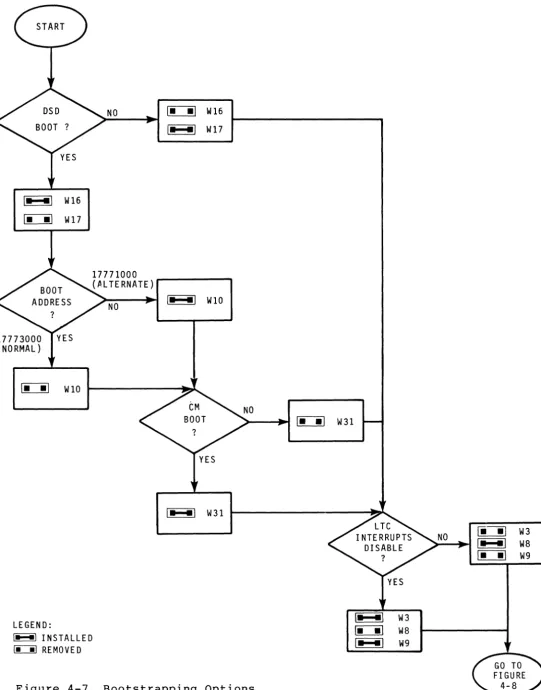
(1) Bootstrapping Options. This group provides jumpers to
enable or disable the built-in boot program (W16 and W17), select boot address (W10) and boot mode (W3l), and control line-time clock (LTC) interrupts (W8 and W9).
(2) Device Options. The jumpers in this group enable or
dis-able the disk (W15) and select disk address and interrupt vectors (Wll). There are also jumpers to enable or dis-able the tape (W12 and W13), select tape address and
interrupt vectors (W18), select tape drive emulation mode (W32), and enable or disable tape drive POCs (W33).
(3) Interrupt Priority Options. The jumpers in this group
select the disk and/or tape interrupt priority level (W20 and W21).
(4) DMA Request Monitor Option. Two jumpers in this group (W6
and W7) enable or disable the option.
(5) Error Correction Option. One jumper (W25) enables or
dis-ables the option.
Figure 4-6 shows the location of the Controller jumpers. Table 4-3 is a reference chart that lists all jumpers, includ-ing those used for testinclud-ing the board at the manufacturinclud-ing facility.
The factory configuration is based on the most common applications used by customers. If this "standard" configura-tion satisfies you, skip the rest of this secconfigura-tion, go to the next section, and mount the board.
I '
I:
Jl __ _
J
W30--[IJ
0 - - W34
W29 - - C I I J C T I - -W28
=--W27
W25--LJ
W5 W4
\
[~J/
W24 W23
\ / / W 3 3
crt
§ - -
W32~W31
W18
W~9
W17~
... k
- W 8 W 1 6
-W15 -;:::;:. - - - W12
W14/
W13
I
W11W10
W3--D
Figure 4-6. DSD 8240 Jumpers
_ / W 2 2
~---W21
~W20
W7~
a
W 6 /
D--W2
W1-D
Table 4-3. DSD 8240 Jumpers
Jumper Shipped Option Class Function (As Shipped)
Wl Installed N/A Factory use
W2 Installed N/A Factory use
W3 Installed Boot LTC Disabled
W4 Installed N/A Factory use
WS Installed N/A Factory use
W6 Removed DMA Request Monitor Disabled
W7 Installed DMA Request Monitor Disabled
W8 Removed Boot LTC Disabled
W9 Installed Boot LTC Disabled
Wl0 Removed Boot Boot: Normal Address
WII Removed Device Disk: Normal Address
Wl2 Removed Device Tape Enabled
W13 Installed Device Tape Enabled
Wl4 Removed Device Disk Enabled
W15 Installed Device Disk Enabled
W16 Installed Boot Boot Enabled
Wl7 Removed Boot Boot Enabled
Table 4-3. DSD 82413 Jumpers (Cont)
Jumper Shipped Option Class Function (As Shipped)
W21 Removed Int. Priority At Level Five
W19 (Not used on this board)
W213 Installed Int. Priority At Level Five
W22 Removed N/A Factory use
W23 Removed N/A Factory use
W24 Removed N/A Factory use
W25 Removed Error Correction Enabled
W26 (Not used on this board)
W27 Installed N/A Factory use
W28 Removed N/A Factory use
W29 Removed N/A Factory use
W313 Installed N/A Factory use
W3l Removed Boot CM Boot Disabled
W32 Removed Device TSV135 Emulation
W33 Removed Device Tape POCs Enabled
W34 Installed N/A Factory use
4.6.3.1. Bootstrapping Options
The secondary set or bootstrap loader, as it is also known, enables the CPU to load complete operating systems and application programs.
The primary boot is contained in the DSD 8ge diagnostic control board. This board contains a program in PROM, which initializes system memory, including parity. It also checks the Controller, Winchester drive, and permits bootstrap load-ing (second boot) from any Winchester volume, the Tape drive,
or a RXe2-compatible floppy - such as DS-lee/leS subsystems.
This primary boot is enabled or disabled with two jumpers. The program can be selected from starting address l7773eee (DEC normal) or l777leee (DEC alternate). One jumper selects this address.
Most DEC LSI-II CPU modules are configured in one of two power-up modes. Some modules may be configured in as many as four power-up modes. Because of these variations, You should consult your DEC documentation for specific details about the CPU module that you are using. As an example, LSI-ll/23
modules can be configured to power-up in modes 1 and 2. The DSD 824e Controller will behave differently depending on the selected power-up mode.
In mode 1, the CPU enters console ODT without attempting
to boot. At that point, the user must manually initiate the
primary boot by typing the address of the boot device. That is, 17773eee or 17771eee for the DSD Winchester boot PROM, or the address of some other device boot PROM in the system.
In mode 2, power applied to the module causes the CPU to internally generate a bootstrap starting address (17773eee) and begin to execute instructions found at that address.
The DSD 824e Controller provides two secondary boot modes: conversational and non-conversational. The
conversa-tional mode prompts the user, via console, to select a device for the secondary boot.
In non-conversational mode, there are, again, differences based on the selected power-up mode. To use the LSI-ll/23
example once more:
• In mode 1, the secondary boot device can be selected, via
console ODT, by typing the device starting address.
• In mode 2, the secondary boot will be obtained from
One frequent problem with DEC CPUs is completing the boot operation while the line-time clock (LTC) is running. This is because some systems use a continuously-running LTC, not
enabled by operating software. In such systems, an LTC
inter-rupt may occur during booting - before proper
interrupt-handling software is loaded into main memory.
If you are using a StacPac Processor module (DS-400), you will not experience any of these problems. If you are using other "Processor" modules you can also prevent these problems by properly using the functions provided by your DSD 8240 Con-troller •
. The following example assumes you are using a LSI-ll/23-PLUS (DEC KDFll-BA) CPU. This illustrates system-dependent considerations that must be taken into account. Refer to DEC documentation for other CPU boards.
The DEC LSI-ll/23-PLUS board includes a bootstrap PROM. This PROM tests memory and allows bootstrap loading from several devices. The confidence checks provided by the PROM are oriented towards the CPU and serial communications link.
If your computer CPU is an LSI-ll/23-PLUS, you have a choice of using the Winchester boot or the CPU boot. However, you must be aware of the following:
(a) The LSI-ll/23-Plus boot PROM and LTC are enabled by a
single jumper (J5) on the board. The DEC CPU responds to LTC address: 1777546.
(b) The DSD 8240 Controller contains circuitry to temporarily
disable LTC interrupts (clamping Q-Bus signal BEVENT L low), until enabled by interrupt-handling software (i.e., a write to location 1777546 with bit 6 set).
Consequently, if you desire to use the DEC KDFll-BA boot, you must:
• Disable the DSD Controller boot and LTC functions.
Conversely, if you desire to use the DSD 8240 boot, you must:
• Disable the DEC KDFll-BA boot/LTC functions (by grounding
J5) and enable these functions on the Controller board.
Consult DEC documentation and use Figure 4-7 to determine the bootstrapping configuration required by your DSD
\_ _\ W16
r:i::::::i] W 1 7
NO ~ W16
\- _I W 17
17771000 (AL TE RNATE)
NO
\- -I
WI0~ WI0 ~---~~
LEGEND:
I- -I INSTALLED
~ REMOVED
\- _I W31
>--... ~
oc::::iJ
W 31NO ~ W3
I- -I W8
~ W9
\- _I W3
~ W8
[image:54.618.21.562.18.708.2]